Electronic design
This week i want to create a echo hello-world board with atleast two additional components a LED and a switch hello.ftdi.44.cad file is the source library. there are 4 free pins in the microcontroller: PB2, PA7, PA2 and PA3.
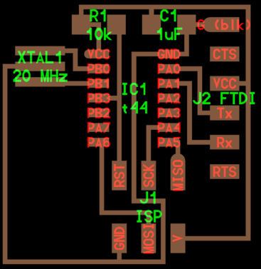
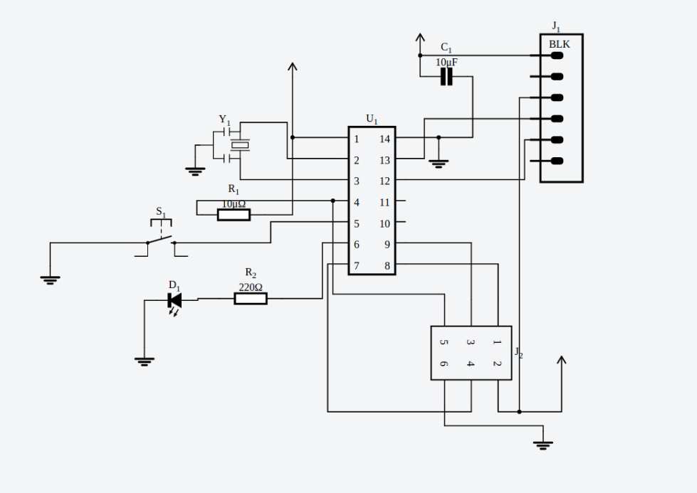
The given is the sketch diagram of the original echo hello-world board
This week i have spent some time on discovering various Electronic components that i can make use of, Neil's lecture helped me to learn about components.I used digikey for knowing about the specification of the components
My idea is to develop an echo.helloisp initially with a additional switch and a LED and then improvise it to some use.
Eagle
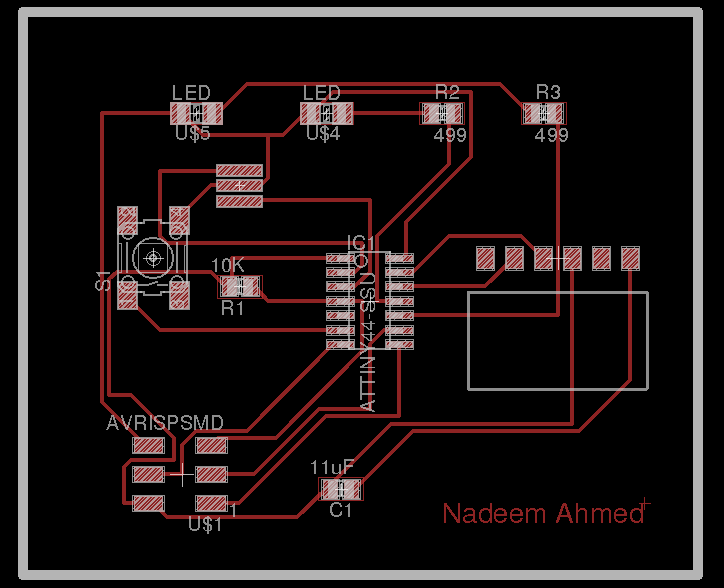
I am going to modify this hello board by adding a LED and a switch
before that i have gone through some tutorials for drawing schematic and the board which was very helpful for me to get started.Adding fab library to eagle
Inorder to access the components that is available in fablab there is seperate library that we should add to get access into these are the steps to follow after downloading eagle:-
- Download fab library (fab.lbr )
- Place it in the installation folder
- Open eagle
Library -> Useand choose the required .lbr fileLibrary -> Update all
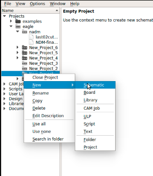
file -> New -> Project
after new project is created in your window right click on the same project and select schematic
Here i list what all materials i needed to make my modified echo.hello board so that i will have a clear idea while adding it to my schematic
Bill of Materials
- Attiny 44
- 20Mhz crystal
- 10k resistor
- 499 ohm resistor
- 1uf Capacitor
- LED(2 Nos)
- press switch
- 2x3 Header
Type "add" and a window will pop-out choose the fab library and select the required components
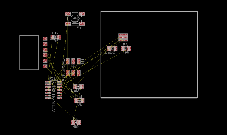
First of all i just replicated the base board that is echo.helloISP board in eagle,here goes the schematic

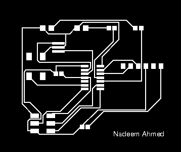
this is how i got the board file when i switched from my schematic to board file (.brd)
now we wanted to route the circuit we have 2 options one is to mannually route and the other is to use the automatic routing
automatic routing
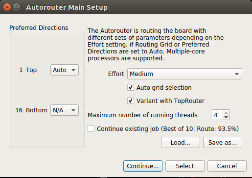
This is the screen shot of the autorouting options, here since this is a single side simple board we only have to enable the top part and such have to disable the bottom surface by choosing the "N/A" option from the drop down menu.
This is how it looks after i added a LED and a switch,i tried both auto and manual routing inorder understand the differance and efficiancy of autoroutung, i felt good with autorouting in eagle but even then at some point of time we may need to manually adjust autorouted one according to our will,
Milling the board
I can make it ready for milling by selecting layers and deselecting all the layers and select only top layer then File -> Export -> image

you will get a pop up like this when you select image here we can choose the name and format ,dpi,type of image,area etc, for milling we need to choose .png format and tick monochrome then click apply, you will get the trace, same way select only dimension layer and export as a monochrome image whcih will be our cut part.
I started milling and everything looks fine to me.. but my board end up in a mess.
i was not able to understand what happend at the first glimpse then realized that its because of the adjustments made in the both net-classes (Edit->Net Classes) setting and design rules (Edit -> Design rules)

there are various contarints like clearance,size,distance. i was not aware of this options where this determines the minimum distance between the component,pads,vias etc. so what happened to my board? My design has such small traces such that my roland was not able to recongnize and mill the same.
i only had to increase the clearance width and other contraints to certain level (approx 16 mil) which will depend on the design and bit we used to mill.
because of the error without knowing the reason first i ended up in redesigning the circuit with about 17 mil clearance(in both netclass and design rules) and i have made a new one like below since i made one i will use this one for now.which looked like this:-

placed the copper clad on modella's bed with the help of double side tape and in adjusted the z axis,in fab modules loaded the image and give it to mill
TADA..!! i got my OWN board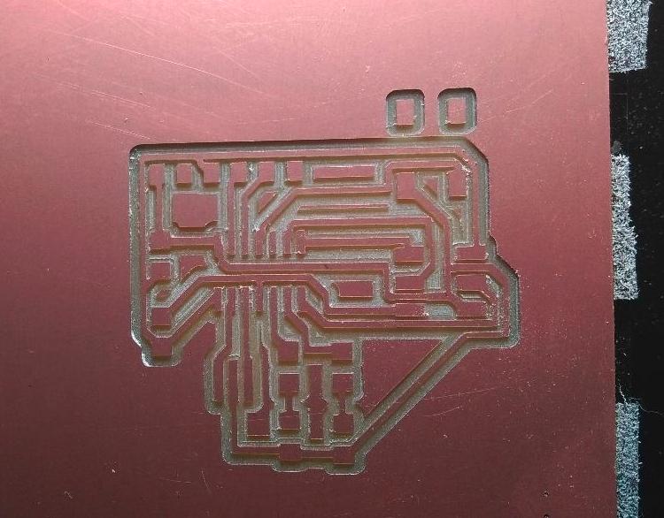
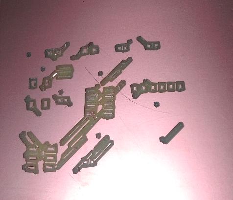
Now i have to stuff the board for that i have collected all the required components from inventory to my SMD collecting plate made by ourself


This is how it looks :-
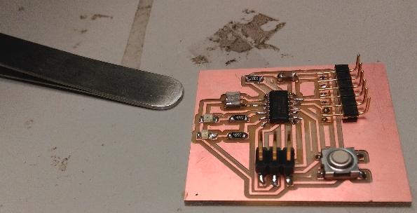
our inventory is running short of FTDI connector.so i am trying to connect with connector header as seen on the pic and its looked like this

You can download my design files HERE..!
Autodesk 123D Circuit
This week i also planned to try out 123D circuit too,open up https://circuits.io/
sign up with an account,then you will have option "New" and you will get this menu as in image if you click new.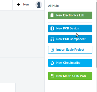
select New PCB design and start adding components for the same in the top right corner you will have a option like add components which is explained the below image
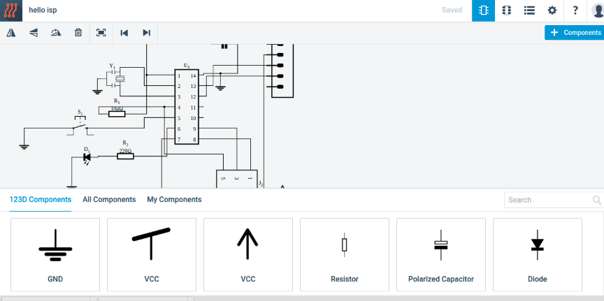
Autodesk 123D Circuits i got all the components from autodesk 123d Circuit
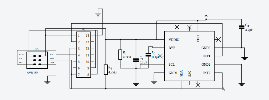
This is replicated base board that is echo.helloISP board in Autodesk 123D Circuit,here goes the schematic
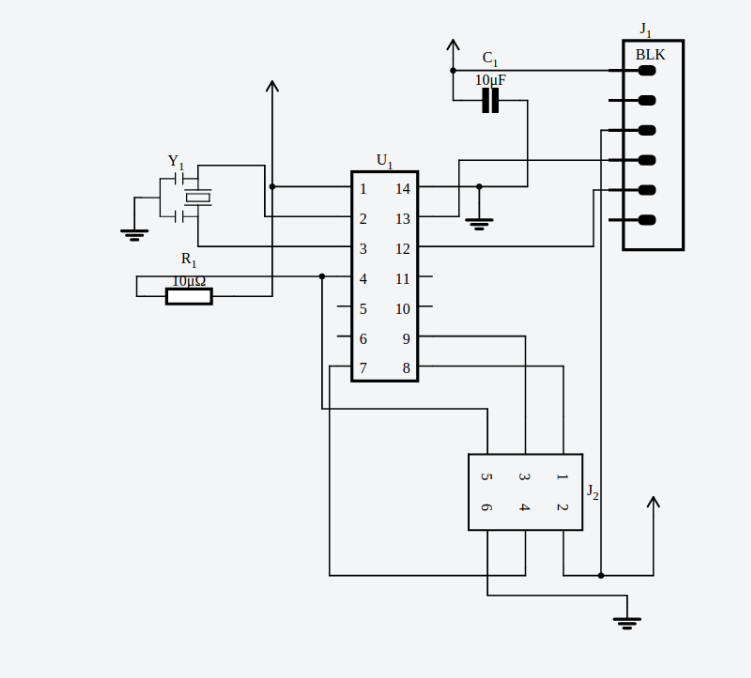
when i embedded LED and a switch using Autodesk 123D Circuit
How can i convert the 123d design to the required format?
,in 123d circuits we will obtain gerber file so we need to use another converter that converts gerber -> png i found many conerting tool both online and offline
from the above image its clear the traces are not that correct, so this wont be a reliable method
Spirit Level with LED Indicator
I just wanted tryout how to build a spirit level using ATtiny tiny and i have found 3 axis accelerometer(MMA8452Q) in my lab inventory and ofcourse LED indicators to reflect level status, I am just giving a try i dont how good it will be, First i am give it a try in the 123D Circuit it felt good for me except there is no auto routing functionality, So we have to mannually route each circuit traces
This is the final schematic i managed to draw with autodesk 123D circuits,Now the one major job is remaining 'routing' this is the finally routed circuit sketch
You can download Files here.