


W4 - ELECTRONIC PRODUCTION
Mission & initial concepts
Assignment
Make the Fab (tiny)ISP incircuit programmer
Learning outcomes:
● Describe the process of production
● Demonstrate correct workflows and identify areas for improvement if required
Have you:
❏ Shown how you made the board
❏ Explained any problems and how you fixed them
❏ Included a ‘hero shot’ of your board
THE PROCESS OF PRODUCTION A ND PROGRAMMING
a) Review Concepts
I am completely new in electronics, so in order to dont be frustrated i decided that i was going to learn from previous fablab students.
I put focus on:
http://fabacademy.org/archives/2015/doc/electronics_production_FabISP.html
Files i used in this assignment
(from Fab lab):
Traces
b) Understanding BOM
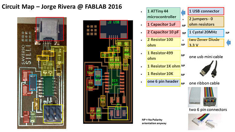
I reviewed each one of the tutorials in order to understand which pieces are needed and which role each one had so i got following list:
• 1 ATTiny 44 microcontroller
• 1 Capacitor 1uF
• 2 Capacitor 10 pF
• 2 Resistor 100 ohm
• 1 Resistor 499 ohm
• 1 Resistor 1K ohm
• 1 Resistor 10K
• one 6 pin header • 1 USB connector
• 2 jumpers - 0 ohm resistors
• 1 Cystal 20MHz
• two Zener Diode 3.3 V
• one usb mini cable
• one ribbon cable
• two 6 pin connectors
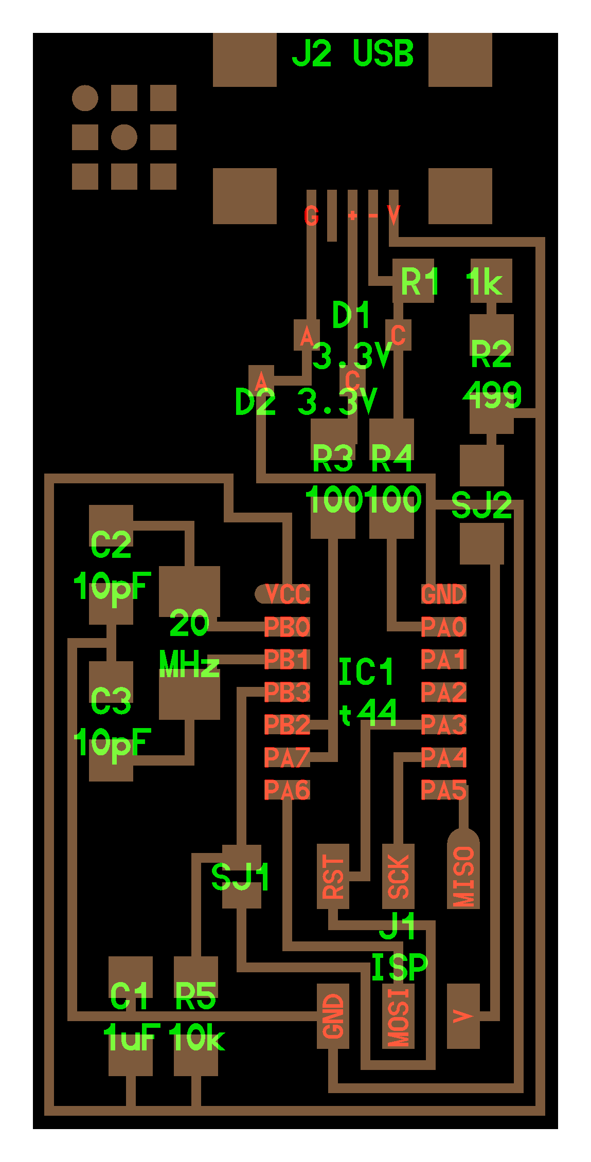
c) Selecting boards and urnderstanding components and polarities
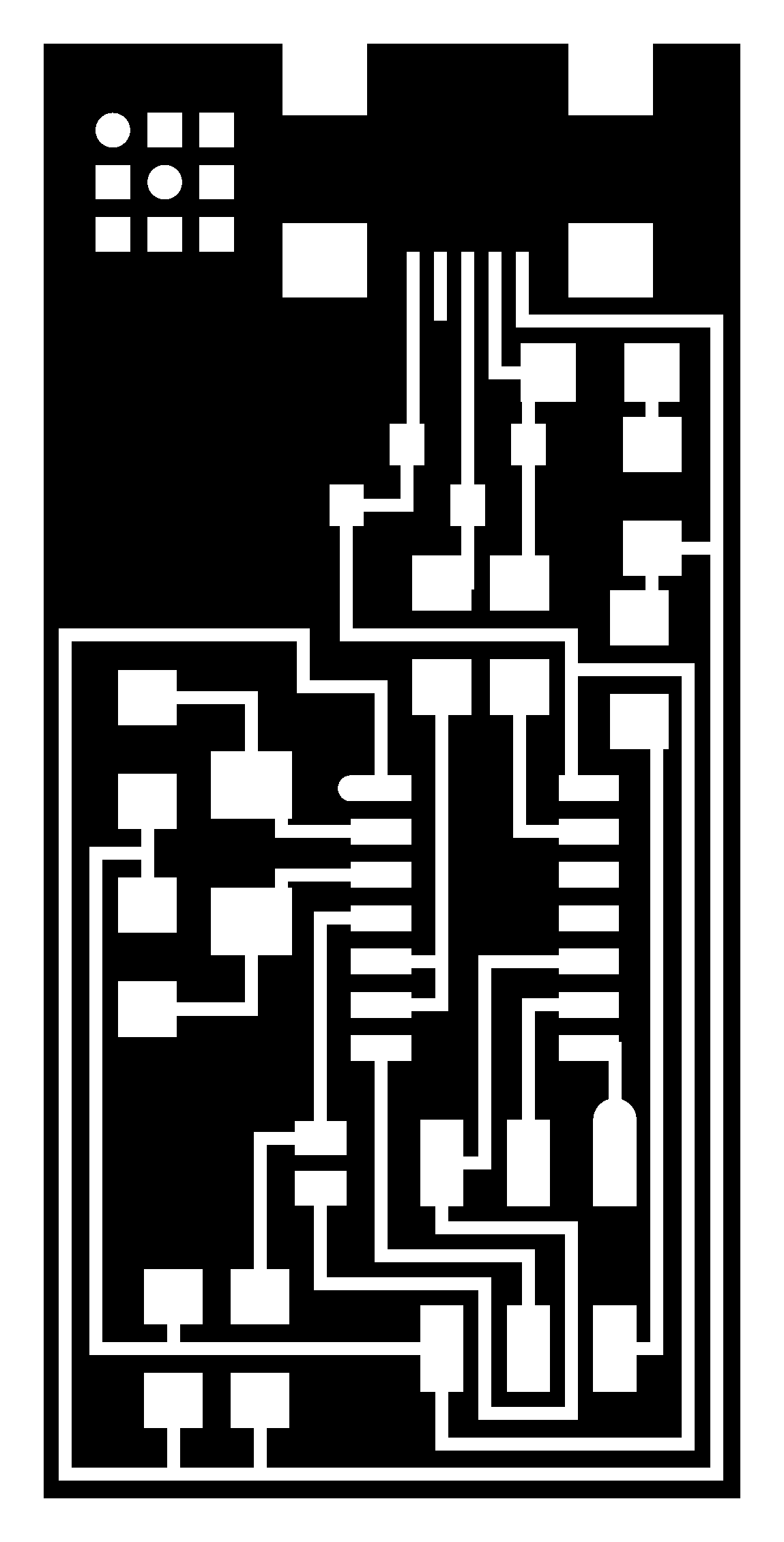
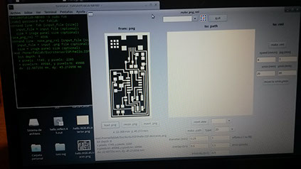
Download the board file and the circuit board trace:


http://academy.cba.mit.edu/classes/embedded_programming/hello.ISP.44.traces.png
http://fabacademy.org/archives/2015/doc/%22http://academy.cba.mit.edu/classes/embedded_programming/hello.ISP.44.png
d) Planning the soldering
The next step is to understand which one are these names and which are the positions in the circuit design. So i create following chart
Also reading the different documentations i understood that the position of some components should be in the right way, so i documented it : Diodes and minicontroller 44 and additionally create and additional diagram over some existing picture
microcontroller 44 : the circle in the microcontroller must be in VCC position.
Diodes : the small line should be alligned with the C in the diagram
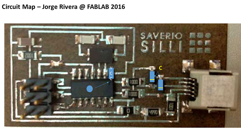
Note : Use Saverio documentation as reference
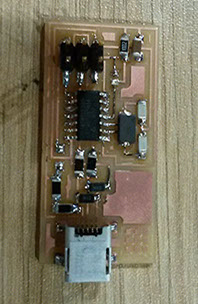
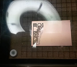
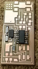
e) Making the board and soldering
With the theory in mind i decided to print the png files and ask for my components, document each one with a label and start practice soldering. I use some photos from previous fablab students to help me in this process.
At first i checked the files and all seems to be ok. But my first output would not be perfect
The process of soldering
Someone in the fablab told me that i should beging soldering from inside (center) to the outside.
I started with the 44 microcontroller having in consideration that there is a circle in a corner that should match with the VCC position (energy)
My strategy for soldering was:
1. Heat the zone target
2. Left a point of tin on it
3. Left the component over the solid tin
4. Use 2 tools each one at each side to heat the tin.
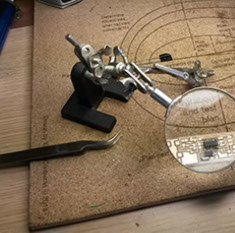
Another problem i had was the size of the component, I used a very small glass to help me.
Finally, i finished my board and now it was time to start programming
OUTLINED PROBLEMS AND HOW I SOLVED
a) Drilling
My first output did not do anything at the right side. So i put down the drill and start again with the process.
After that the card was ok.
The next difficult point was the dimension of the components,
I finally solved it using an small but very potent glass.

-crop-u1634.jpg)

b) Planning
I experimented two difficult moments:
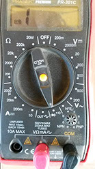
a) At some moment i had a confusion with the components because of a non planified movement of the table, So i had to reorder the mayority of them. A multimeter helped me for recognizing the capacitors in the position A (photograph)
c) Soldering
At another moment when i started soldering i thought i made a mistake soldering two components that do not have to be close. The position B (photograh) make a sound (beep) if it is the case. I helped me to avoid these kind of problems.
.jpg)
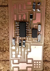
Testing and fixing the board
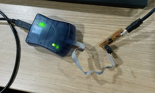
When my board was finished i connect it with the programmer so i can verify it was right.
At first it doesnt work. I remember i had some problem with one of the jumper and had a feeling that there was a problem. So after using the multimeter it confirmed that.
The jumper (J!) was fixed and now it showed me the green light.
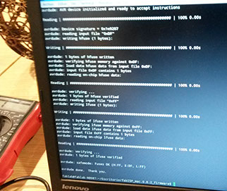
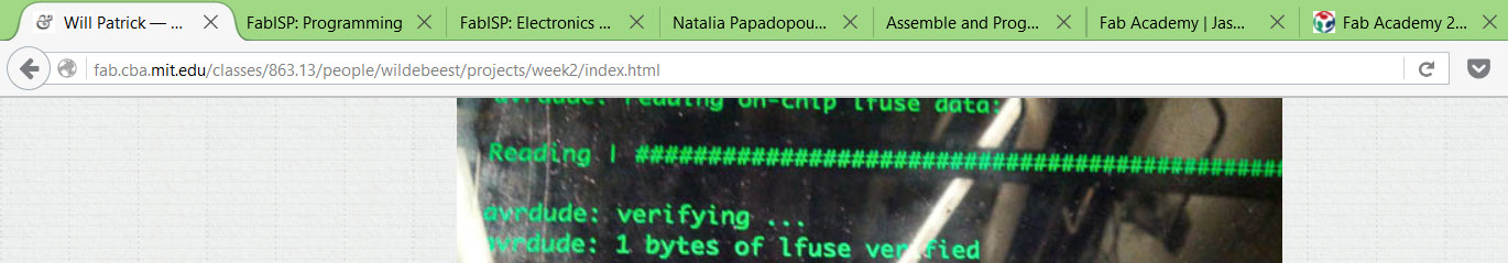
PROGRAMMING THE FAB ISP
We had the firmware already downloaded in a laptop, so programming was just a matter of going over the commands. Everything went fine,
make clean
make hex
sudo make fuse
sudo make program
It fuses ok.
In order to use it as a FabISP, i removed the soldier on JS1 and JS2
