Objectives:
- Redraw the echo hello-world board and at least a button and LED. Intro, Design, Milling, Bom and Downloads, Soldering, Testing
Intro
The assignment of the week was to design make and test an hello board.
During this week i challenged myself to build an ATxMega based Dev. Board.
In our lab we have some ATxMega 8e5 TQFP32 package, the advantage of the Atmel ATxMega family over the ATMega is the higher clock speed, more accurate ADC ecc.
I wanted my Dev. Board to have an internal voltage regulator ( the xMega 8e5 runs at 3.3V ), an external reset button, FTDI headers , PDI headers and every usable pin exposed.
Some useful links:
Design
To design the board i used Autodesk EAGLE software. Before starting i had to create the ATxMega 8e5 device because it wasn’t available even inside the Atmel official library.
To create a device on eagle you have first to create a symbol which is the device you use on the schematic and the package. Since the package is the TQFP32 ( same as the Atmel 328p ) i only had to modify the pads size because the 1/64 end mill was too big to separate the pads. The last step was to create the device in which you tell eagle how to connect the symbol pins to the package pads.
To create the symbol i referred to the image i found inside the datasheet of the ATxMega.
To name the two GND pins with the same name i used the GND@1 and GND@2.


Below you can see the creation of the Device and the resize of the package pads from 0.05 x 0.022 inch to 0.05 x 0.016.


Since is out inventory we don’t have the standard LM3480im3-3.3 voltage regulator but we have the NCP1117 i had to create another component to match the pinout.
You can see the pin difference below.

To design the reset circuit, the PDI headers and to size the decoupling capacitors i followed the ATxMega 8e5 Schematic Check-list you can find at the beginning of the page.
I also inserted a 3 pin header ( to use with a jumper ) to select the input power supply between the USB and the 2 pin header.
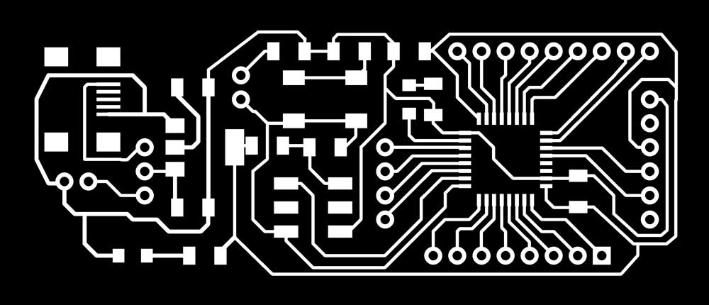
It took me some times to route all the board in a single layer layout but at the end this are the results:
Schematic:

Board:

Milling
I configured the DRC ( Design Rule Check ) to match the end mill we have in our lab ( 1/64 inch / 0.4mm ) and fixed the flaws.

After i exported the board as image with a resolution of 1000 dpi and selecting the monochrome check. I exported the top and pads layers to mill the etching and the dimension layer to mill the holes and outline.
To create the milling file i used the new fabmodules LINK, selecting the 1/64 end mill for the traces and 1/32 end mill for the outline and holes.
Here's the pcb after the etching and milling routine.

Soldering
I started soldering the components from the voltage regulator and before soldering the ATxMega i checked if the VR output was correct.

To check the output i connected an external 12v power supply to the board power input pins and with the voltmeter i checked the output.

Next i soldered the remaining components.

BOM and Files
| Name | Quantity | Code |
|---|---|---|
| ATxMega 8e5 | x1 | IC1 |
| NCP1117 3.3 VREG | x1 | US3 |
| 100Ω Resistor | x3 | R2, R4, R6 |
| 10kΩ Resistor | x2 | R1, R3 |
| 0Ω Jumper Resistor | x1 | R5 |
| 10μF Capacitor | x1 | C2 |
| 100nF Capacitor | x4 | C1, C3, C4, C5 |
| LED SMD | x2 | D1, D2 |
| 6 pin SMD header | x1 | JP1 |
| Mini USB SMD | x1 | |
| Button Switch | x1 | S1 |
| Male Header M2 | x1 | J1 |
| Male Header M3 | x1 | J7 |
| Male Header M4 | x1 | J3 |
| Male Header M6 | x1 | J5 |
| Male Header M8 | x1 | J6 |
| Male Header M9 | x1 | J4 |
Downloads
Schematic.sch ( 82kb )
Schematic.brd ( 332kb )
ATmel library with patch atmel.lbr
Fab library with NCP1117 fab.lbr
READ FIRST
The schematic here doesnt work straight out of the box please see below for more info.
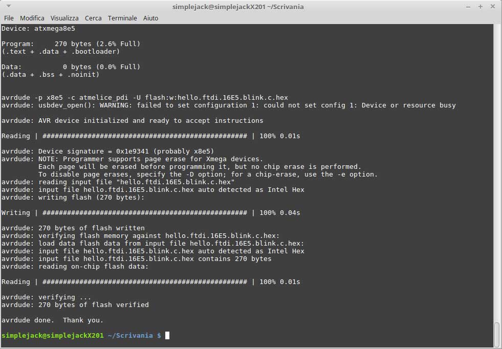
Testing
To test the board i used the Atmel ICE programmer
http://www.atmel.com/tools/atatmel-ice.aspx?tab=overview
I had, from week 4, the avrdude toolchain already installed, and the Atmel ICE it's recognized by default from Linux. I downloaded the Neil’s .c and .make files and i modified the latter to fit my programmer and IC.
                PROJECT=hello.ftdi.16E5.blink

                SOURCES=$(PROJECT).c

                MMCU=atxmega8e5

                F_CPU = 32000000

                TARGET = x8e5

                PROGRAMMER= atmelice_pdi

                CFLAGS=-mmcu=$(MMCU) -Wall -Os -DF_CPU=$(F_CPU)

                $(PROJECT).hex: $(PROJECT).out

                  avr-objcopy -O ihex $(PROJECT).out $(PROJECT).c.hex;\

                  avr-size --mcu=$(MMCU) --format=avr $(PROJECT).out

                $(PROJECT).out: $(SOURCES)

                  avr-gcc $(CFLAGS) -I./ -o $(PROJECT).out $(SOURCES)

                program: $(PROJECT).hex

                  avrdude -p $(TARGET) -c $(PROGRAMMER) -U flash:w:$(PROJECT).c.hex

Since the Atmel ICE does not provide the power to the board i used the jumper to select the input source from the USB connector. I connected the 6 pin PDI connector to the board and the led on the Atmel ice became solid green.
I ran the make -f hello.ftdi.16E5.blink.make
and after make -f hello.ftdi.16E5.blink.make program
The code didn’t load up and got an Error ( unfortunately i forgot to take a screenshoot ) it was related so some physical connection failure. I tried changing the PROGRAMMER= atmelice_pdi to other programmers names but still got some errors. http://www.nongnu.org/avrdude/user-manual/avrdude_12.html
After doing some testing and giving a better read to the datasheet i found out that the capacitor that goes from the reset line to ground ( 100nF ), since the PDI programmer use the reset line as clock line, was smoothing the clock and making the programmer unable to synchronize. I cutted the external reset circuit bus and tried again with atmel studio.
Notes: (from the datasheet) The pull-up resistor makes sure that reset does not go low unintended. When the PDI programming and
debugging is used, the reset line is used as clock. The reset pull-up should be 10kΩ or weaker, or be
removed.
The pull-down resistor prevents from overvoltage on the RESET pin when the switch is pressed.
Any reset capacitors should be removed if PDI programming and debugging is used. Other external reset
sources should be disconnected.

New design
I redesigned the board adding a jumper to isolate the 100nF reset circuit and resized the pull-up resistor on the reset line from 10kohm to 4.99kohm.


BOM and Downloads
| Name | Quantity | Code |
|---|---|---|
| ATxMega 8e5 | x1 | IC1 |
| NCP1117 3.3 VREG | x1 | US3 |
| 100Ω Resistor | x3 | R2, R4, R6 |
| 10kΩ Resistor | x1 | R3 |
| 0Ω Jumper Resistor | x1 | R5 |
| 10μF Capacitor | x1 | C2 |
| 100nF Capacitor | x4 | C1, C3, C4, C5 |
| LED SMD | x2 | D1, D2 |
| 6 pin SMD header | x1 | JP1 |
| Mini USB SMD | x1 | |
| Button Switch | x1 | S1 |
| Male Header M2 | x2 | J1, J2 |
| Male Header M3 | x1 | J7 |
| Male Header M4 | x1 | J3 |
| Male Header M6 | x1 | J5 |
| Male Header M8 | x1 | J6 |
| Male Header M9 | x1 | J4 |
Downloads
etching.png 1000dpi ( 58kb )
holes.png 1000dpi ( 40kb )
Schematicv2.sch ( 78kb )
Schematicv2.brd ( 330kb )
ATmel library with patch atmel.lbr
Fab library with NCP1117 fab.lbr
I milled the new board and soldered it. After i tried to program it with the Atmel ICE on the Atmel Studio IDE and it worked. As you can see on the photo the capacitor’s jumper is not connected so that the board can be programed flawlessly.


Testing on Linux with avrdude toolchain
To program it i downloaded the .c file and the .make file and modified them to suit my ATxMega 8e5 IC next, with the commands below, i flashed the program to the board.
make -f hello.ftdi.16E5.blink.make
sudo make -f hello.ftdi.16E5.blink.make program