Output devices
For this week the assigment is to add an output device to a microcontroller board you've designed and program it to do something
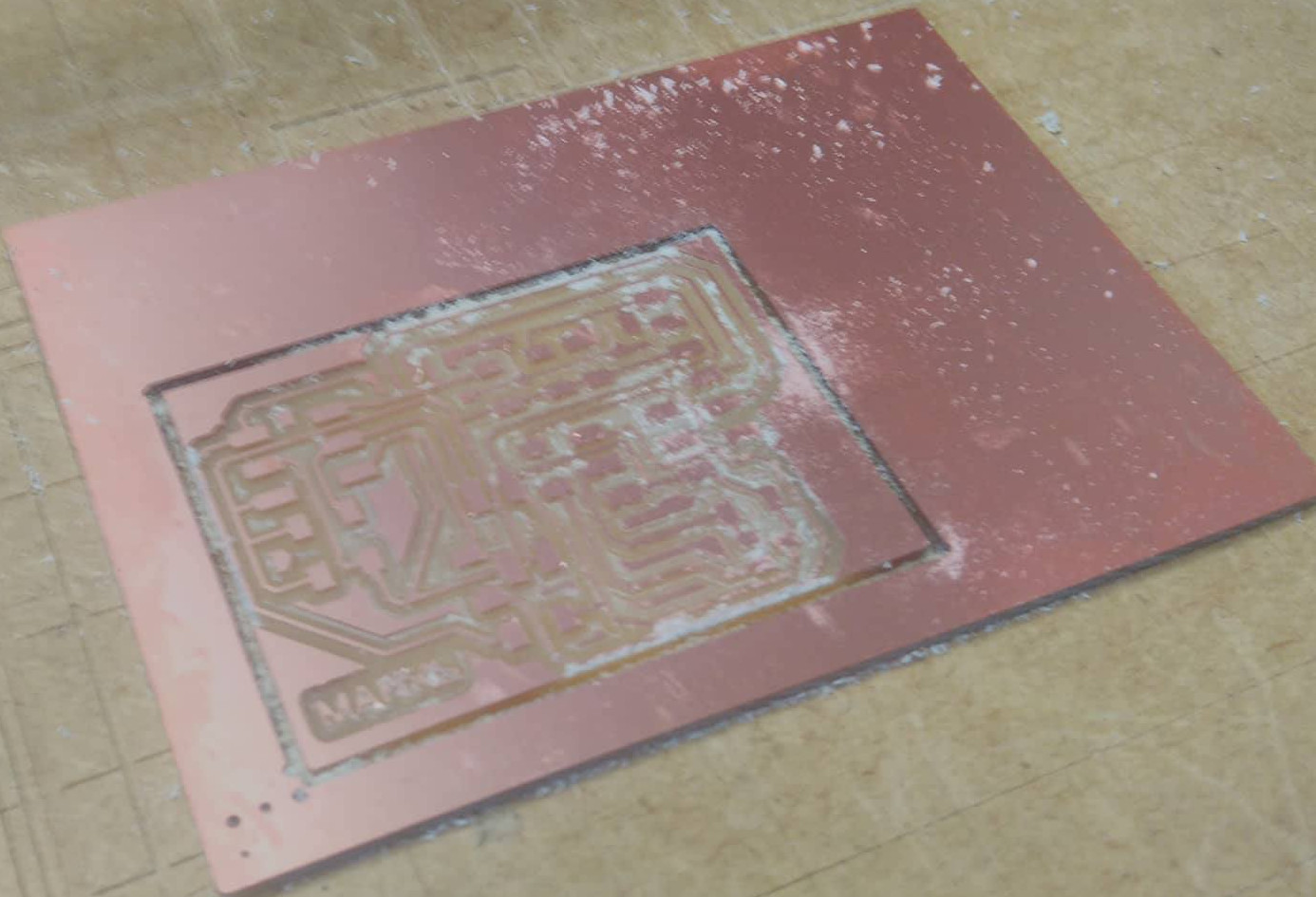
Make PCB
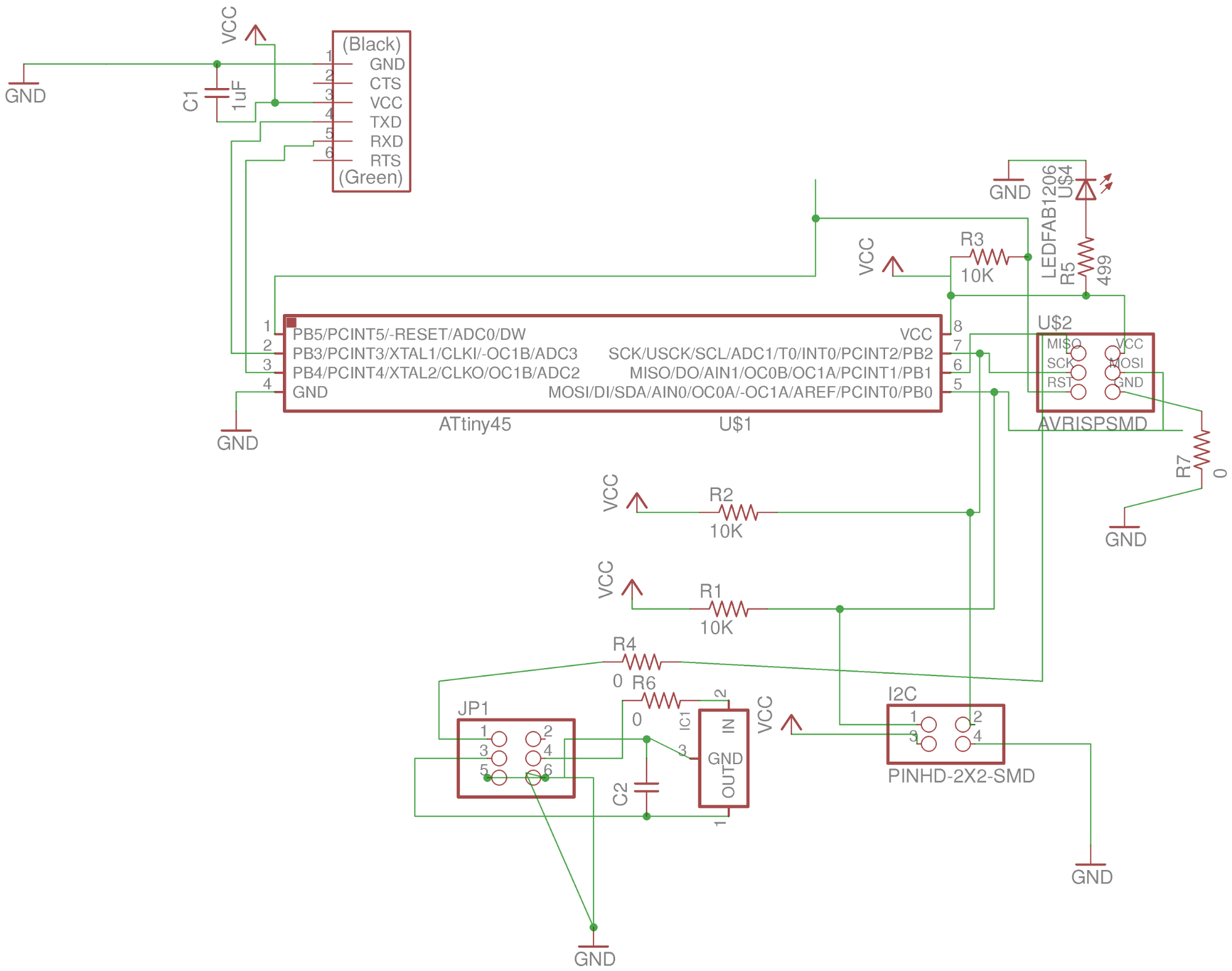
This week I decided to make a output device which will control a servomotor. This circuit was based on the weekly class and I2C communications. But it has slight modifications as:
- Use ATtiny45 instead ATtiny44.
- Not use a external clock and only use an internal clock of 8Mhz.
- Servomotor has own power supply.
- Add pins for future I2C communications
BOM
- (1) Attiny45
- (3) Resistor 0hm
- (3) Resistor 10KOhm
- (1) Resistor 499 Ohm
- (2) Capacitor 1uF
- (1) led blue smd
- (2) Connector 2x3
- (1) Connector 2x2
- (1) Connector 6x1
- (1) I2C regulator 5V 1A
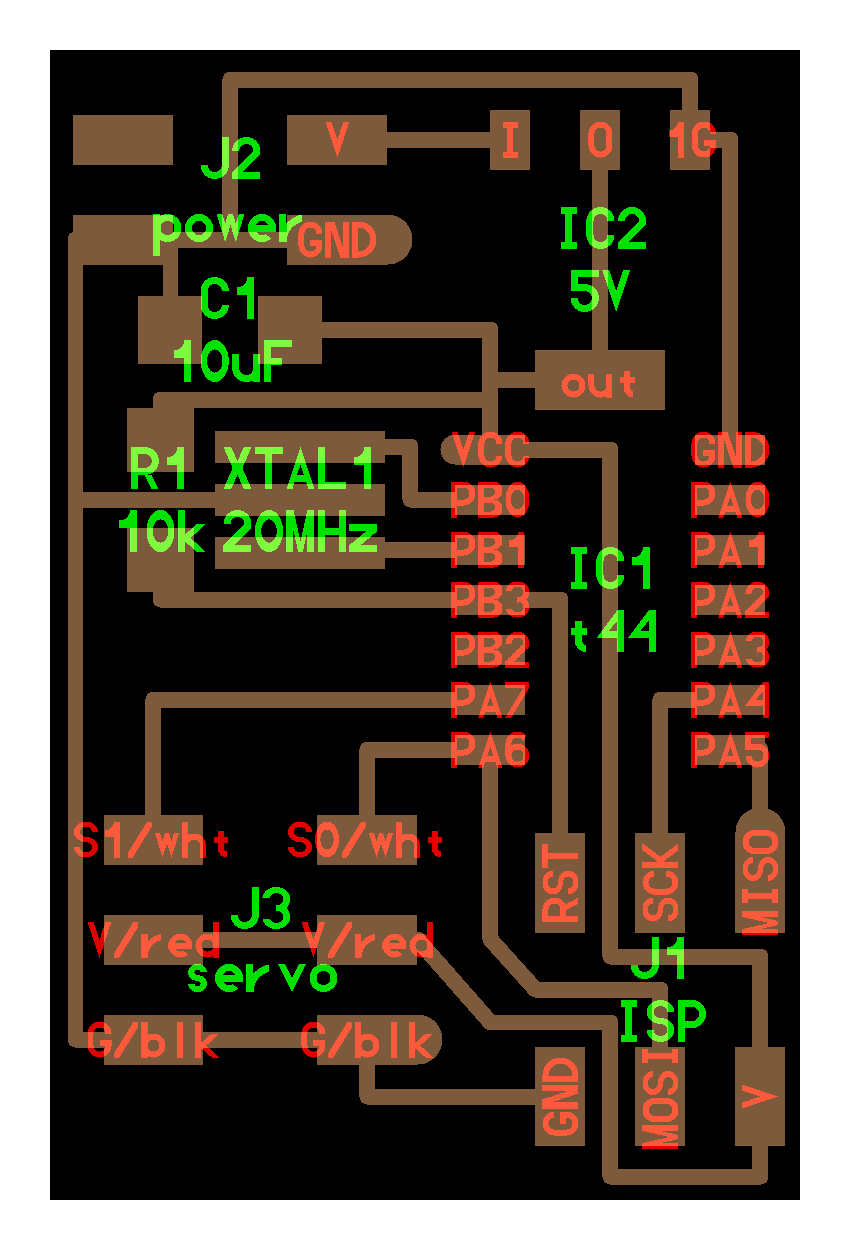
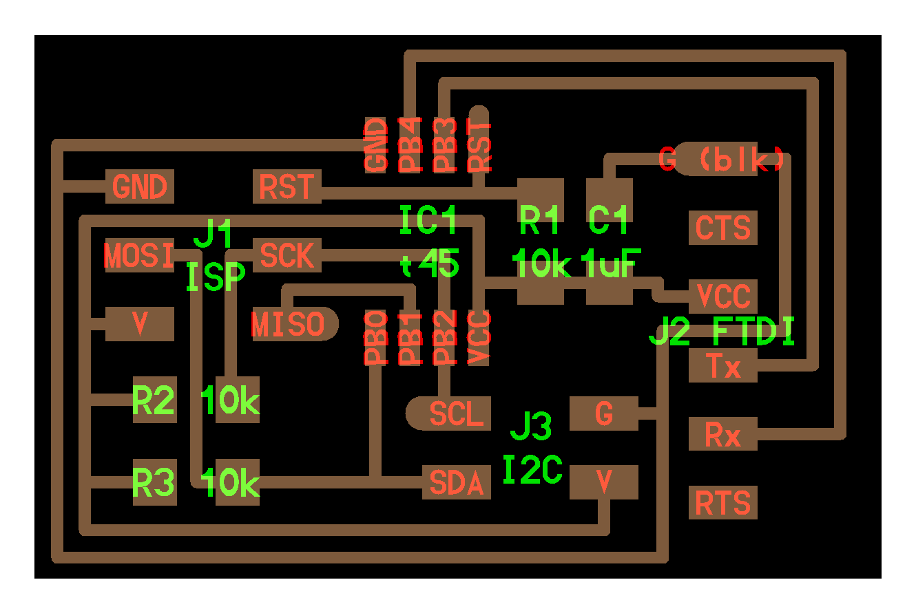
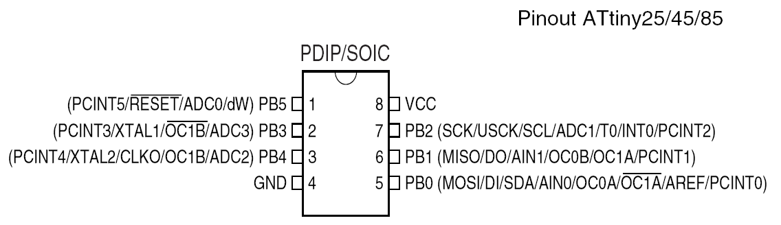
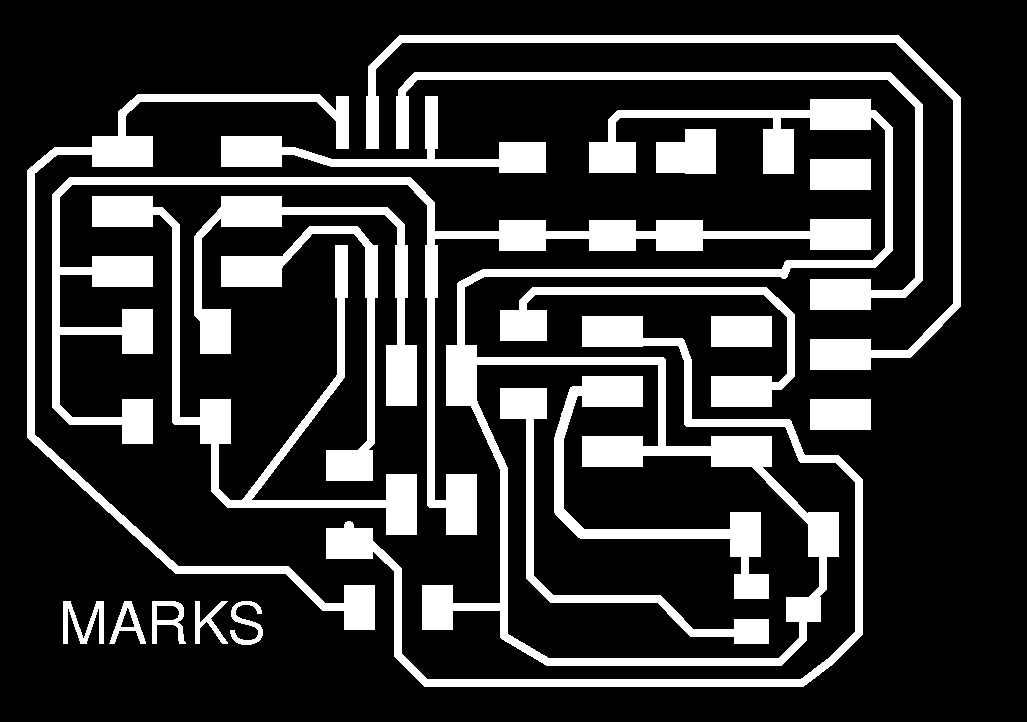
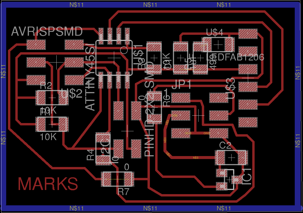
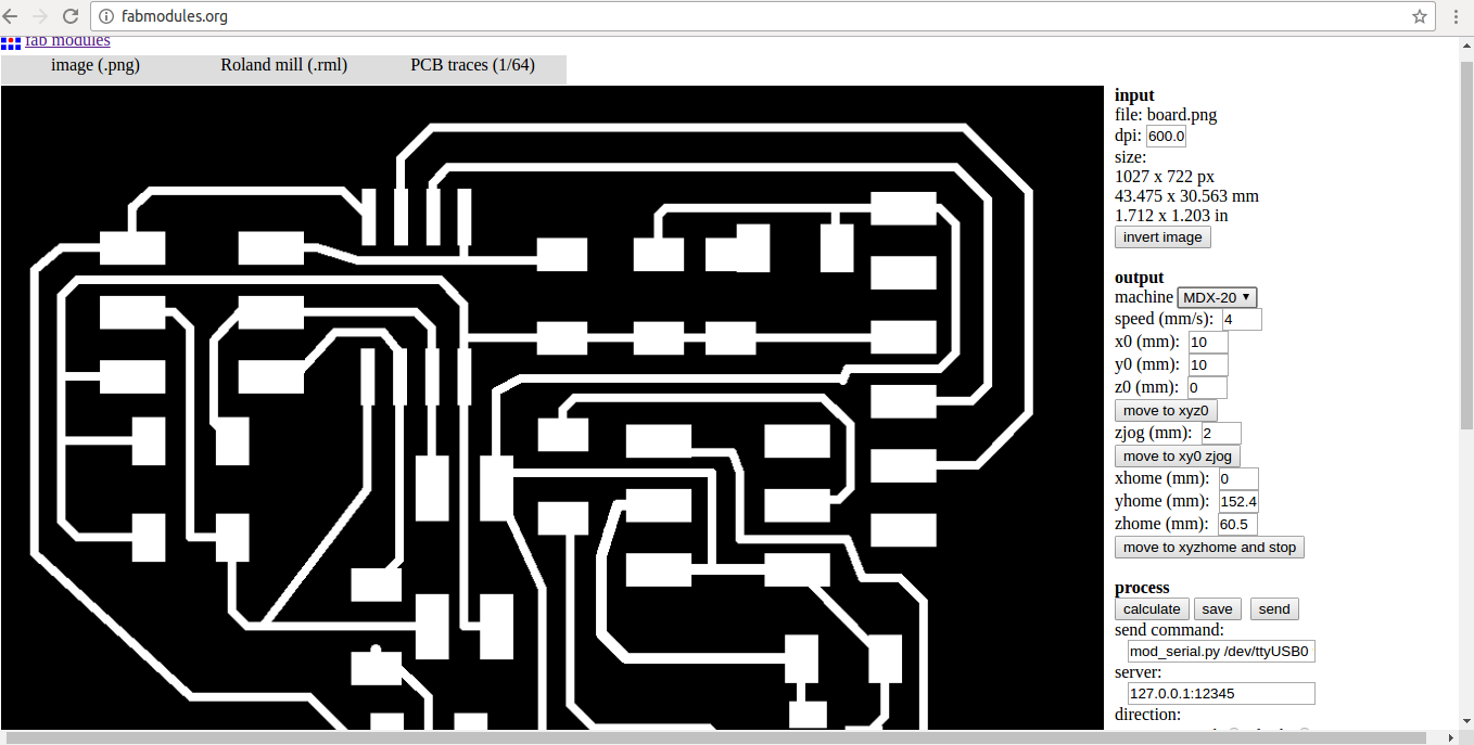
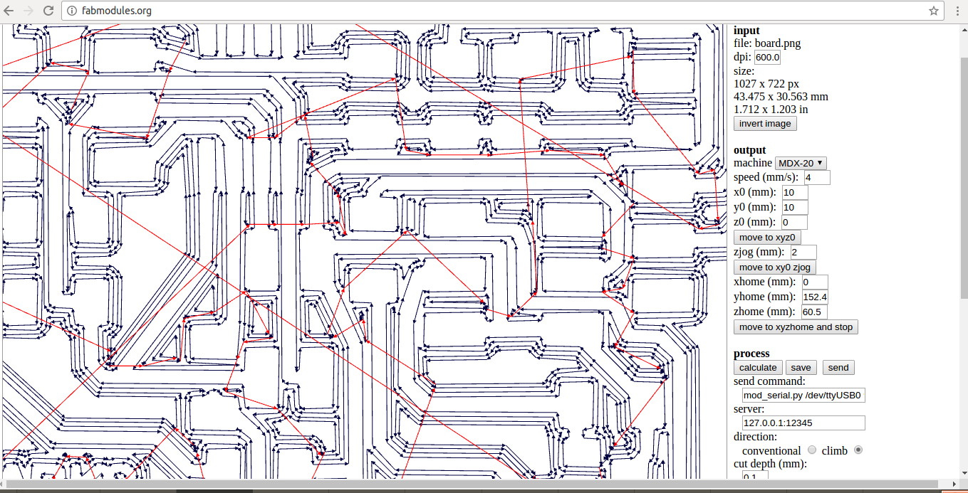
The ATtiny45 datasheet shows two pins with PWM modes, ICSP protocol and I2C communications. Then, we link these pins in the circuit. The datasheet can download here. I have designed the PCB in Eagle software. The images below are results of our design. The image left shows the elements links, the middle image is prepared to mill in the Roland machine, and after finding union traces in fabmodules , we have correct the traces. Finally, we got right circuit without mistakes in its traces.
The images right shows the process to obtain a .rml file on fabmodules. It will send to Roland Machine. But before it, we check the traces to find union paths.
Finally, we got the PCB to solder the electronic elements. The eagle files can download here
Programming microcontroller
We decided to program Attiny45 in C. So we read the Attiny45 datasheet .
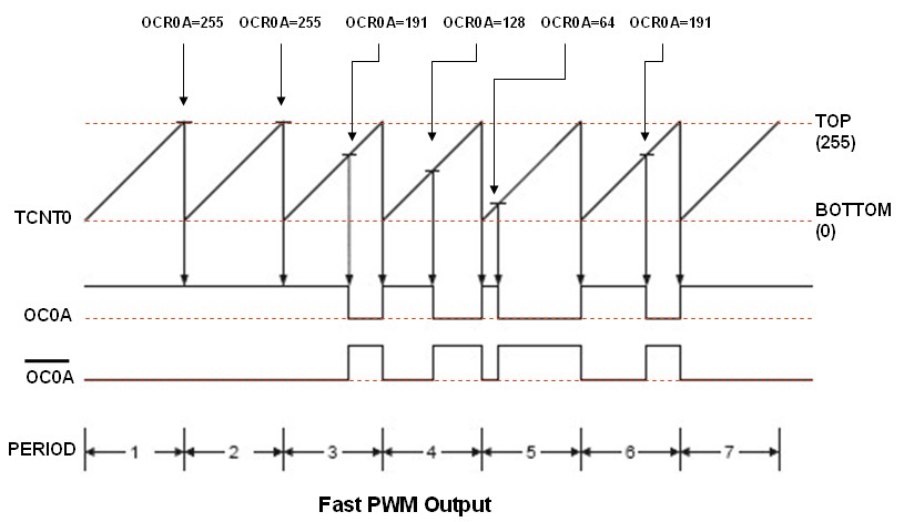
Additionally, we watched a video about FASTPWM because Attiny45 implements this PWM mode.
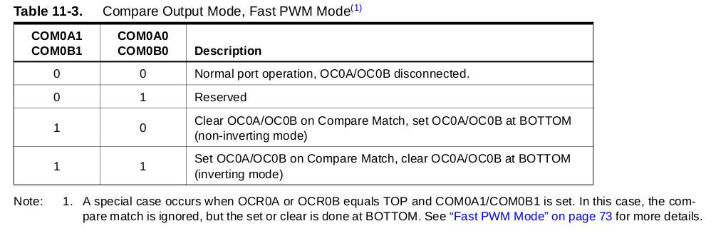
The registers to setup are TCCR0A and TCCR0B. The table 11-3 shows how fast PWM mode should setup
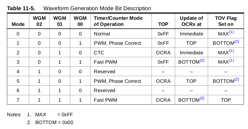
 The bits to waveform generation mode represents in the next table 11-5
 The pin 1 used to implement PWM which scales with clock and formulate with the equation
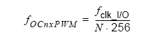 In the equation fclk_I/O is the current clock of Attiny, in this case is 8MhZ and N is a modernizr-2
scalar division setup by clock bit. The next table details differents scalars. In our experiment selected N=1, the
new frequency was 32KhZ. The source code is
In the equation fclk_I/O is the current clock of Attiny, in this case is 8MhZ and N is a modernizr-2
scalar division setup by clock bit. The next table details differents scalars. In our experiment selected N=1, the
new frequency was 32KhZ. The source code is
#define F_CPU 8000000

/*
io.h provides lots of handy constants
delay.h provides _delay_ms and _delay_us functions
*/
#include <avr/io.h>
#include <util/delay.h>

int main()
{
	/*
    Port B Data Direction Register (controls the mode of all pins within port B)
    DDRB is 8 bits: [unused:unused:DDB5:DDB4:DDB3:DDB2:DDB1:DDB0]
    1<<DDB1: sets bit DDB1 (data-direction, port B, pin 1), which puts PB1 (port B, pin 1) in output mode
    */
    DDRB =  1<<DDB1 ;

     /*
    Control Register A for Timer/Counter-0 (Timer/Counter-0 is configured using two registers: A and B)
    TCCR0A is 8 bits: [COM0A1:COM0A0:COM0B1:COM0B0:unused:unused:WGM01:WGM00]
    2<<COM0A0: sets bits COM0A0 and COM0A1, which (in Fast PWM mode) clears OC0A on compare-match, and sets OC0A at BOTTOM
    2<<COM0B0: sets bits COM0B0 and COM0B1, which (in Fast PWM mode) clears OC0B on compare-match, and sets OC0B at BOTTOM
    3<<WGM00: sets bits WGM00 and WGM01, which (when combined with WGM02 from TCCR0B below) enables Fast PWM mode
    */
    TCCR0A |=   1<<COM0B1 | 0<<COM0B0 | 0<<WGM02 | 1<<WGM01 | 1<<WGM00; //no invertign configuration

    /*
    Control Register B for Timer/Counter-0 (Timer/Counter-0 is configured using two registers: A and B)
    TCCR0B is 8 bits: [FOC0A:FOC0B:unused:unused:WGM02:CS02:CS01:CS00]
    0<<WGM02: bit WGM02 remains clear, which (when combined with WGM00 and WGM01 from TCCR0A above) enables Fast PWM mode
    1<<CS00: sets bits CS01 (leaving CS01 and CS02 clear), which tells Timer/Counter-0 to not use a prescalar
    */
    TCCR0B |= 0<<CS02 | 0<<CS01 | 1<<CS00; // pre-scale factor 1

    //f_pwm = f_clk/(N*256) = 8000000 Hz/(1*256) = 32Khz

    int ipwm ;

    while(1)
    {
    	/*
    	 OCR0B = 50; //  OC1B + Duty = 50/255 *100% = 19.6%

    	//make pwm pins outputs
    	DDRB |= (1 <<DDB1);
    	_delay_us(1500); //2ms
    	DDRB |= (0 <<DDB1);
    	_delay_us(18500); //18ms
		*/

		ipwm = 0;
		while(ipwm <= 255){
			OCR0B = ipwm++;
			_delay_ms(2); // delay 2 millisecond
		}

		ipwm = 255;
		while(ipwm >= 0){
			OCR0B = ipwm--;
			_delay_ms(2); // delay 2 millisecond
		}
		_delay_ms(100); //delay 100 millisecond
    }

	return 0;
}
The result is show in the next video