FAB LAB
Puebla

ELECTRONICS DESIGN
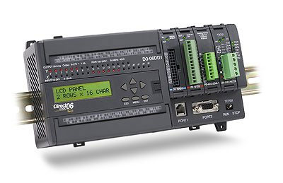
In Fablab Puebla we work with many small and medium sized enterprises and one of the difficulties they're faced is dealing with the control of their electronics have to do with the control of high powered tools. So my idea for final project was an affordable and open source PLC(programmable logic controller)
The plc must be,not in any specific order:
- Affordable.
- Open source
- Compact.
- Easy to program
- Easy to use.
- Flexible
The steps to create this project are the following
- Define the different needs to apply to the PLC
- Design the electronic schematic
- Manufacture the PCB
- Design and build a packaging
- Program the PLC
Microcontroller
The PLC will contain the following
-
-
-
- 8 digital inputs of 24V DC
- 4 analog inputs of 24V DC
- 8Digital outputs of 127V AC/DC.
- The PLC will also have an entry for Ethernet so that it may communicate
- It must be programmable by USB.
- 2 AC phase controller
- Supply Voltage of 3.3VDC, 5VDC, 24VDC or 127VAC.
-
-
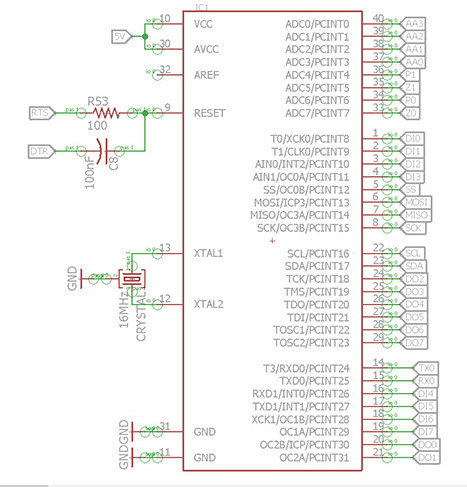
The first thing to do was to choose the microcontroller that would power the PLC, my option were between, the ATMEGA1284, the ATMEGA328 and the ATMEGA2560 so i did a comparison of the three
Comparison
Here’s a quick breakdown of three chips… The 328P powers the Uno, the 2560P powers the Mega 2560, and the 1284P is the ‘Filling’ chip, nestled right in the middle–EXCEPT for RAM. It has an abundance of RAM (16k!) which is important because RAM is typically the resource you run out of the quickest.
Feature 328P 1284P 2560P
Price $2.99 $4.66 $11.28
RAM 2k 16k 8k
Flash 32k 128k 256k
EEPROM 1k 4k 4k
UART 1 2 4
IO Pins 23 32 86
Interrupts 2 3 8
Analog Inputs 6 8 16
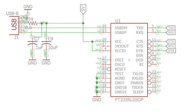
Now that i had a micro the next decision was finding a way to program it, so I decided for a FTDI chip in my case the FT232RL and a USB-B port following the classic arduino boards.
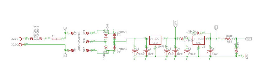
Now for power supply i decided for a transformer which lowered the voltage to 24v, then rectified it an trough regulators obtained the desired voltages.
After that i designed both inputs and outputs parts for the PLC. For the Outputs I decided to have two types the first ones were the good old reliable relays, as they isolated the load, were relatively cheap and could work with both AC and DC loads.
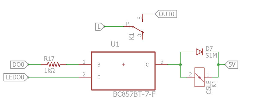
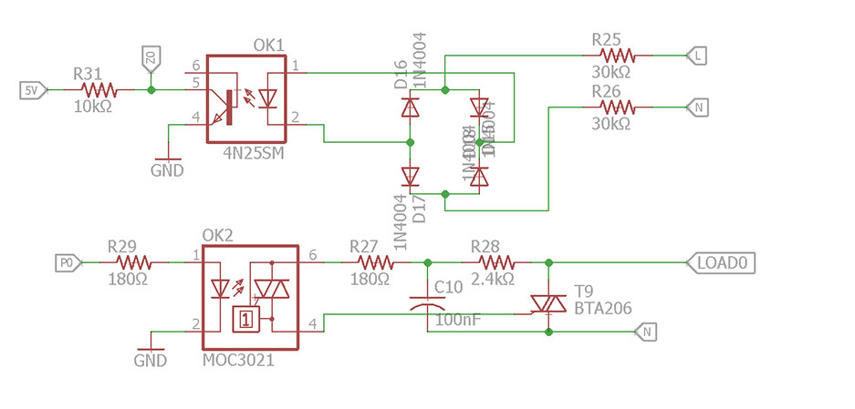
The second type of Output is a phase controller so that small businesses could dim lights or control small AC motors without the need of extra hardware, this was made in two part the first par is a circuit which detects the pass trough zero from the line, this was made using High power resistors to reduce the current, 4 diodes to rectify the signal, an opto-coupler called 4N25 in which the inside photo diode was activated sending a signal so the arduino can detect it. The second part was the on/off part. After the arduino had detected the zero it would send a signal to turn on the opto-triac after x amount of time making sure only the part of the wave needed was used. The opto triac then would activate a suitable triac for the load which would take the bulk of the power needed. Finally i added a snubber circuit which is basically a capacitor and resistor, so it would protect from voltage spikes.
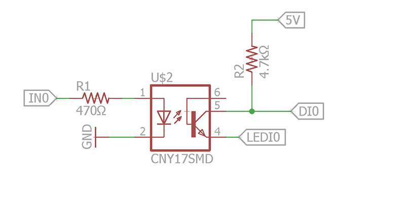
For Inputs i also made two type digital and analog, for the digital ones I used an optocoupler, where I would receive a maximum of 24 volts, and a minimum of 5 so that with the help from a resistor I could regulate the current and not burn the diode. This optocoupler was chosen specifically so that when it eas at its maximum voltage 24 volt, it would have 47mA which is well within the optocoupler parameters.
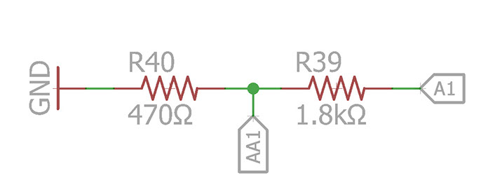
For the analog input i used a simple voltage divider using the formula
Vout=Vin(R2/R1+R2)
so that when it's 24 volts it becomes 5 an so on.
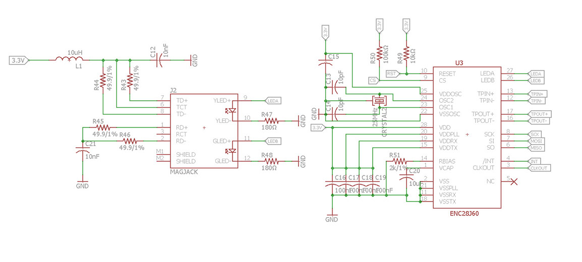
Now that we have supply, the micro-controller, how to program it and both inputs and outputs we could say our PLC is complete, however one very important part of the PLC is that in case it's missing anything you can communicate with external hardware and that's where communications come in specifically Ethernet connection. Which i had already worked with during my Networking assignment. So basing myself on ethernet modules i decided for the ENC28J60 for the main ethernet controller, to use and following the circuits for it i ended up with the next diagram
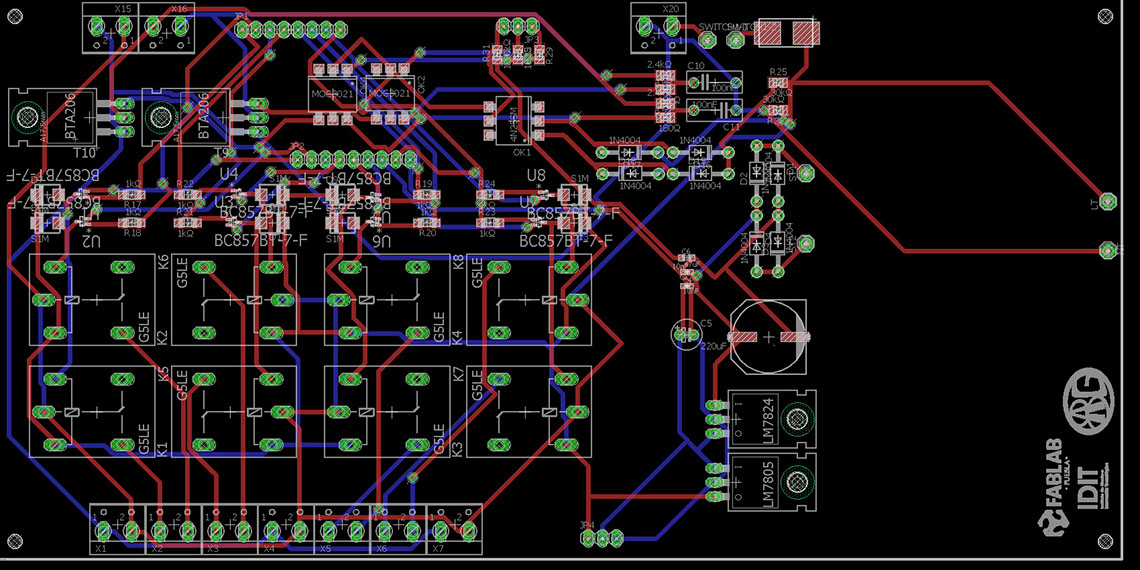
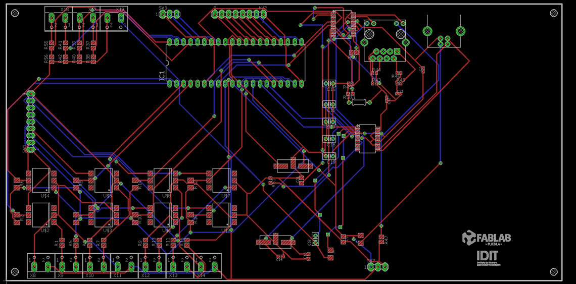
Having all the schematic designed it was time to pass it onto boards. Hoever I soon realized it was too big an complicated for one board only so I separated it into two different boards which would be connected trough cables. Which resulted in the next boards.
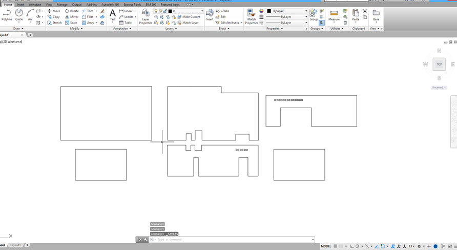
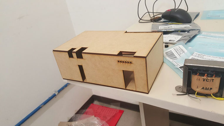
With all the circuits design done, components selected it was time to make the box it will contain in, I opted it to be lasercut and i drew it in auto cad
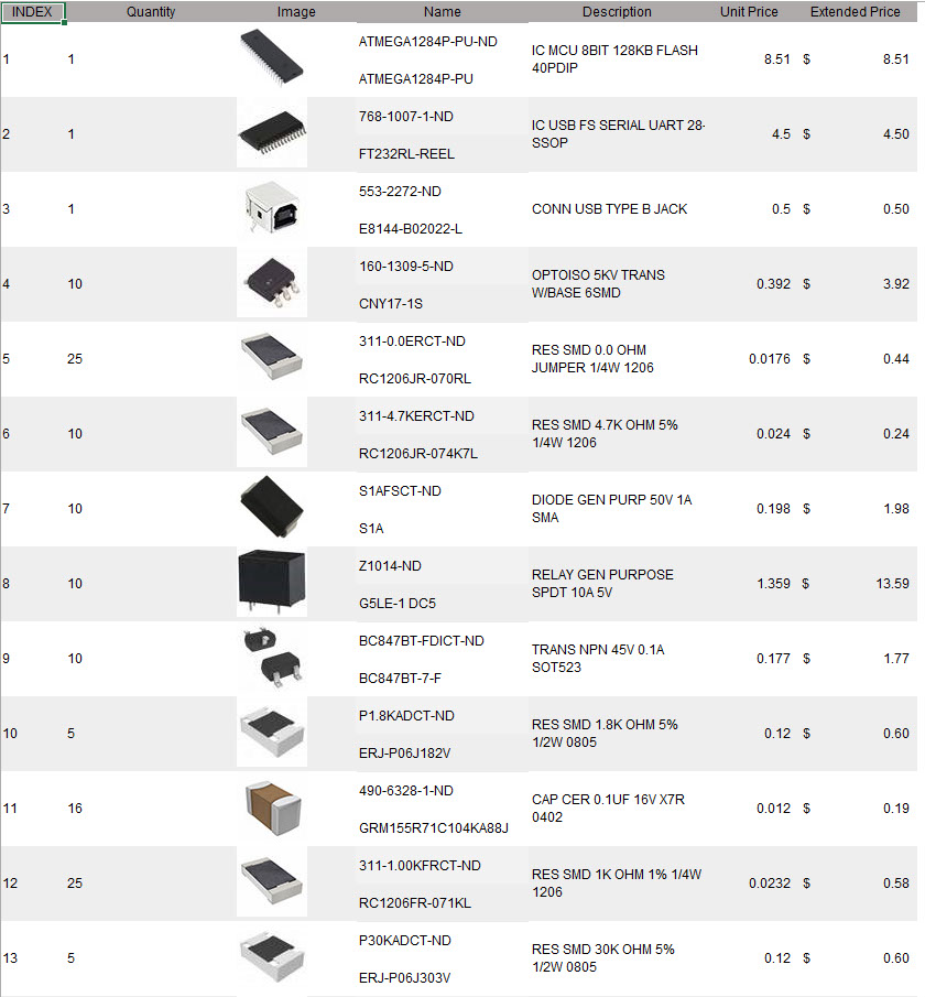
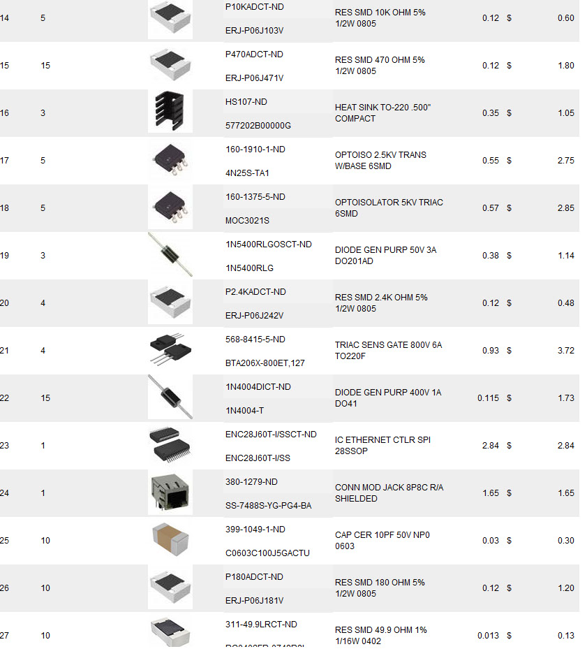
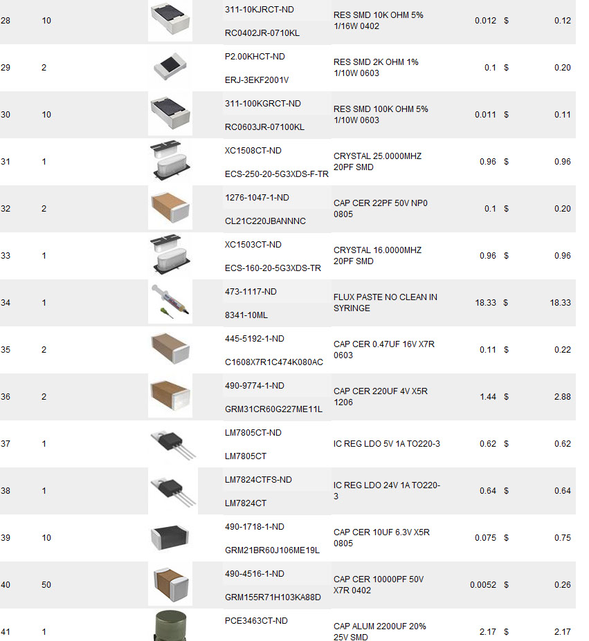
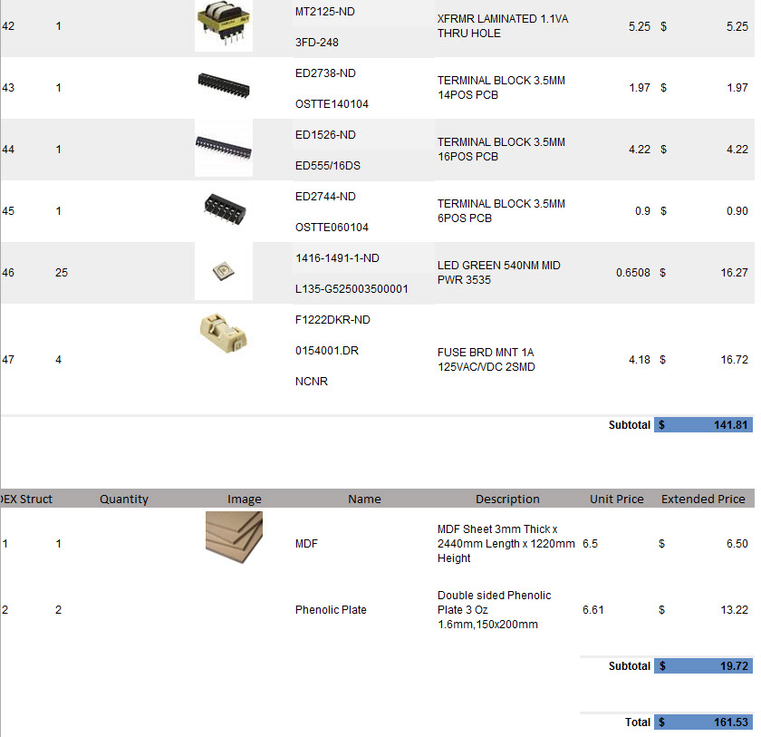
The next step was to buy all components, as I lived in Mexico the components were difficult to find here in electronic stores so what I did was buy them from Digikey. However the MDF i buyed in Home Depot. Here's the list of everything i buyed.
Having the design, It was time to build it.
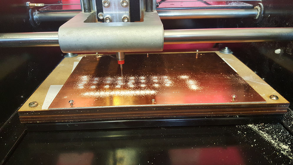
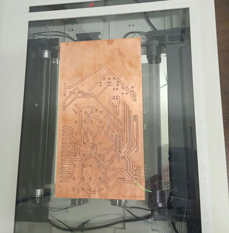
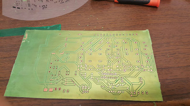
Now with all components ready it was time to build it, it was going to be the first time i tried doing double sided PCBs on the CNC milling machine so what i did was cut my phenolic plate the exact size of the working area for the machine and then align the zero. After that i made 6 perforations just outside the area i was gonna work with and using screws i secured my phenolic plate. After that I started all perforations as if any perforation made after the engraving would damage my circuit.
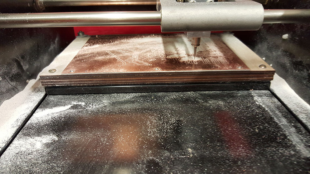
After making the perforations for any trough hole components, I satrted the engraving, for one face, when it finished I used the screw holes I had made as reference to put the other side of the PCB, obviusly i had to mirror the board so that it would be coincident with the first face.
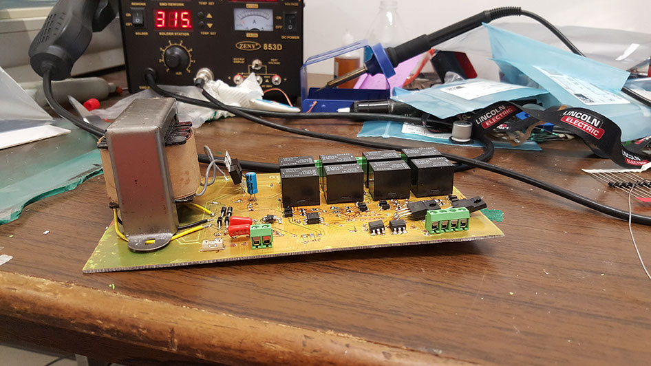
After the milling this were the results
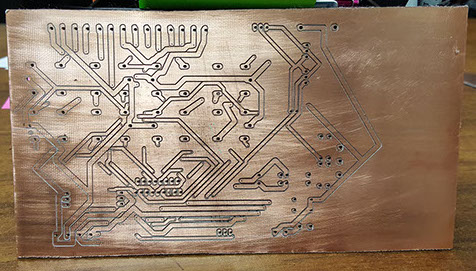
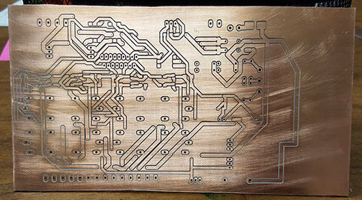
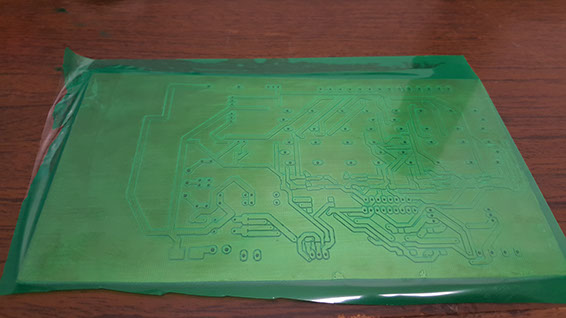
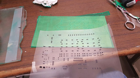
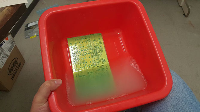
The PCB was slightly moved however considering one PCB of this size goes for around 150 dollars it was quite the good result. I repeated the process for the second board, and the next step was making sure both sides in one PCB were connected. For this I used a conductive ink to pass the electricity. Also as i has quite a few small smd components it was necessary to give it a solder mask so that soldering wouldn't quite be a problem. As my experience with paint solder mask wasn't exactly stellar and this PCBs were quite time consuming and difficult to make i opted for the easier photosensitive film instead. I used UV light to cure and the pads to protect the tha parts i didnt want to be cured. After cruing the film i tossed it into the revealing chemical to remove any unwanted film from pads.
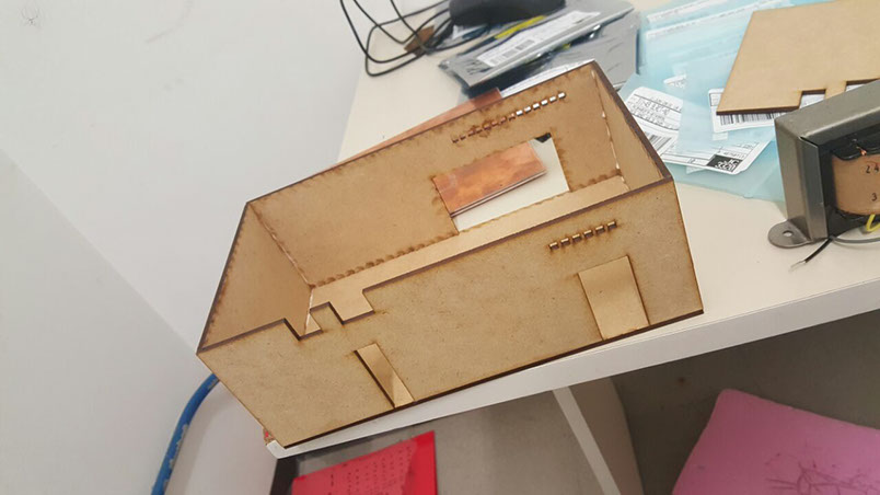
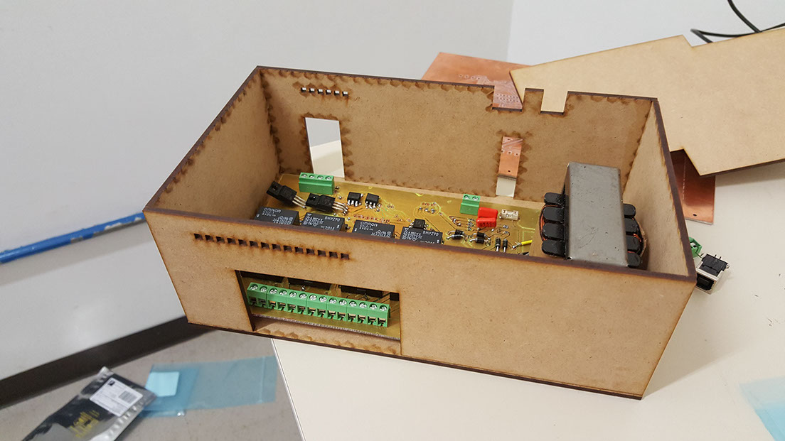
While it was revealing i decided to do tha box for the PLC so i went to the lasercutter with my 3mm MDF and started cutting.
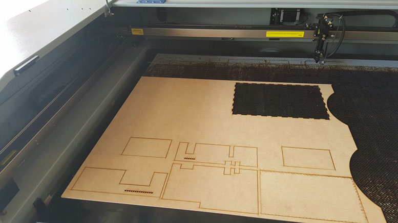
While it was revealing i decided to do tha box for the PLC so i went to the lasercutter with my 3mm MDF and started cutting. And then i started gluing it together.
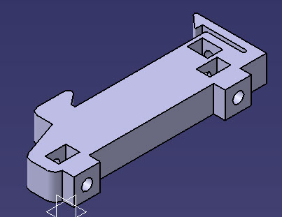
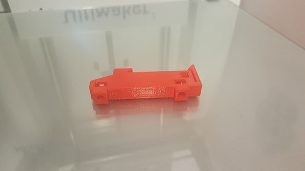
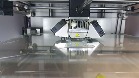
Now I also need something to mount the PLC, the standard are DIN rails so I designed and 3D printed a Din rail mount
By this time the revealing agent had don its work.
So I started soldering my components
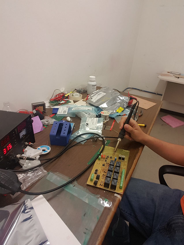
After soldering the first PCB I decided to test the sis omy box and how it would resist the weight of the circuit.
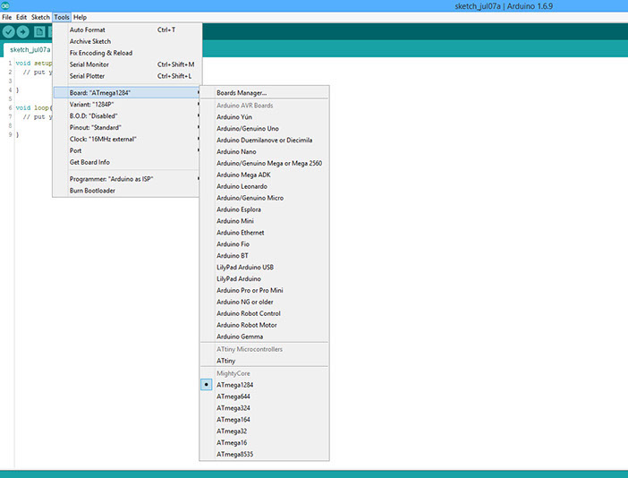
So I has my hardware waiting i need my software now. So as i needed it to work with the programmer i had made I decided to burn the bootloader for the 1284P i=which i downloaded from the Mighty1284 page by arduino. Burning the bootloader was trivial as I just used the arduino ISP, to burn it.
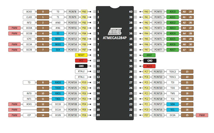
After that what i ended up with was with the next configuration of pins ready to just be programmed away with any old programmer.
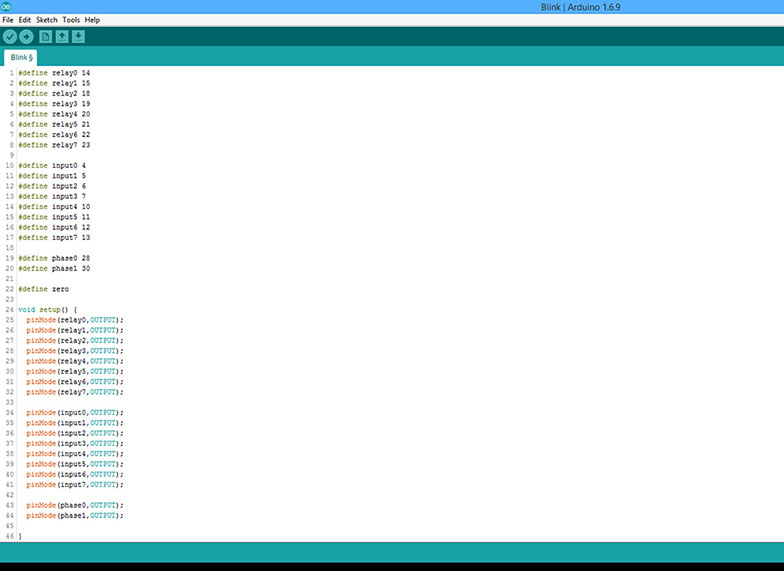
An example of a code for the PLC would look like this
Now finally I leave the video for the process, and a conclusion that even with experience with electronics this was the most ambitious I've ever had on various accounts, starting with all the math I had to do to figure out how it would work, secondly the production was brutally difficult as probably my fablab is ill prepared to create circuits this complex. Specially the double sided milling was hard as well as the resolution was a bit lacking from using the CNC milling machine, maybe in the future we could upgrade the fablab with new equipment to better ourselves in the circuits area.