Electronics Design
Assignment
- Redraw the echo hello-world board
- Add (at least) a button and LED (with current-limiting resistor)
- Check the design rules, and make it
Installing Eagle
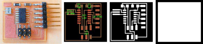
The assignment is to redraw the Hello-world board and add at least one button and led. I am going to draw the board in Eagle - www.cadsoftusa.com . KiCad would also be an option but I am not 100% sure how the Fab part library is working in that program, so Eagle it is. The four pictures above show the basic Fab Hello-World board and layout with no extra components.
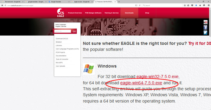
I downloaded the "eagle-win64-7.5.0.exe" file for my Windows 10 operating system and went through the install process, everything worked fine. After I imported the Fab Part Library from Fab Academy schedule page I went into Eagle and saved a test document. Then Eagle made a folder located in "C:/User/myname/eagle". I made another folder inside that folder called "custom library". Then I put the library file (fab.lbr) into that folder.
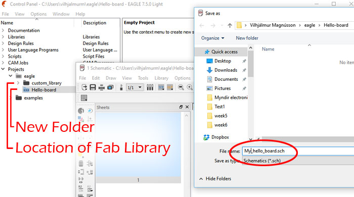
I could find the library in the Eagle (Control Panel mode) in the "Project folder" after the process ahead (see picture). Next move was to make new project: "File/New/Project", I named it "Hello-board". I right clicked on that new folder and clicked on "New/Schematic". I needed to save a schematic file into the new Hello-Board folder: "File/Save as/My_hello_board.sch" (see picture).
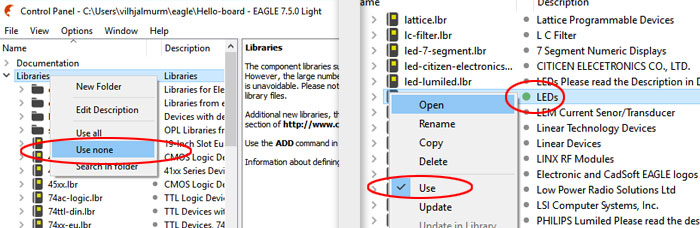
Next step was to hide all the libraries that I would not use. Right click on the "Libraries folder and choose "Use none". Then I activated four libraries by right clicking on them and hit "Use": Those are the libraries that I activated: Led.lbr, Rcl.lbr, Supply1.lbr, V-Reg.lbr . Library is active when gray dot gets green.
I found out when I was beginning to draw my board that I forgot to activate the Fab library. So remember to activate that as well in the "Project" folder inside Eagle.
Drawing the board
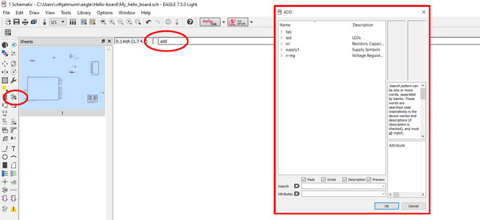
First thing to do when drawing a board in Eagle is to add components into the canvas. To open the library I did click on the "Add" button but I also like to use the command window and write add and hit enter to open it. Inside the library we should see five different libraries and one of them should be Fab library.
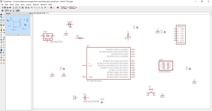
I added those components from the libraries:
Fab Library: 6MM_SWITCH6MM_SWITCH, ATTINY44-SSU, AVRISPSMD, CAP-US1206FAB, FTDI-SMD-HEADER, RES-US120FAB, RESONATOR.
Led Library: LEDSMT1206
Supply1 Library: VCC, GND (+ and - not components).
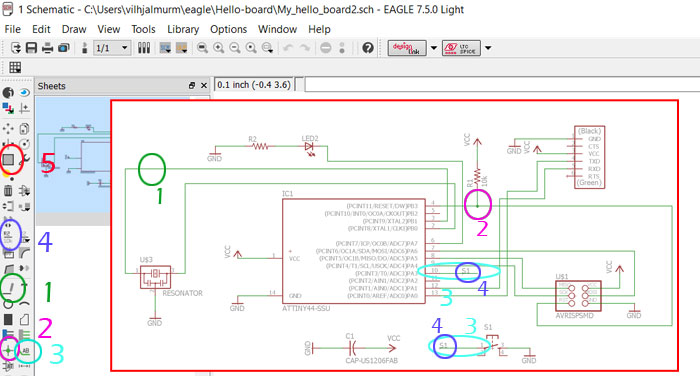
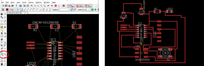
In the next step I connected the components using the "Wire" button in the tool pallet. (Green circle #1). This virtual wiring is a preparing for making the board traces but we will draw the traces in another window, later in the process.
Because this is not the actual traces the line can cross each other, they are not connected when they do. If we want to connect them we use the "Junction" button and a small green dot is placed on the connection (Purple circle #2).
To make drawing more simple it´s possible to connect them with Label button (#3). You have two lines that are not visually connected but when you label them they are connected. It´s done in three steps: Step one make the lines. Step two use Label button and click on the both lines. Step three use the Name button (#4) and name both connections with the same name. Then a small window opens and asks if this is a right connection, click OK.
When I was working on this drawing I needed to group components, lines and move them. I used the Group button (#5), selected all that I wanted to select and hit the Ctrl button on my laptop and right clicked on the mouse to move the grouped items.
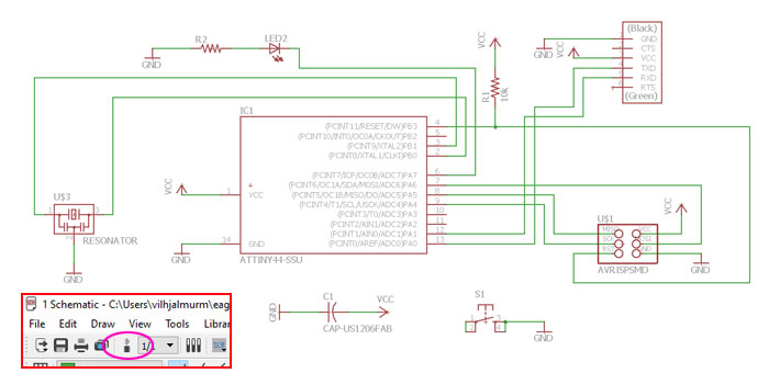
When the drawing was ready I clicked on the "Generate/Switch to board" button in the top panel and a new window appeared. I was ready for the next step to draw the board traces.
The task here was to draw traces and use the "Route"button
from the tool bar. The Yellow lines are guide lines and they can be recalculated if you move your components on the canvas. To do that you use "Ratsnet" button (Is not on this picture). If you need to delete traces you cannot use Trash button only use "Ripup" button that is located right next to "Route" button in the tool bar.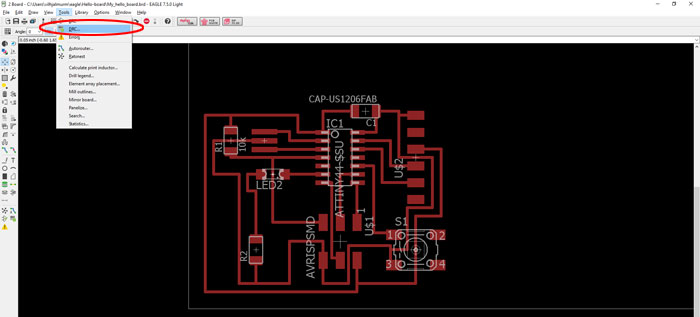
It was really difficult to find the right path for the traces so they would not overlap. When I had finished the puzzle, the next move was to set settings for the traces and run a check. So I clicked on Tools/DRC in top tool bar.
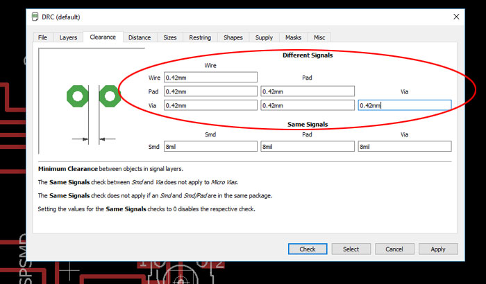
In "Clearance" tap I dialed in 0.42mm in all boxes regarding Different Signals.
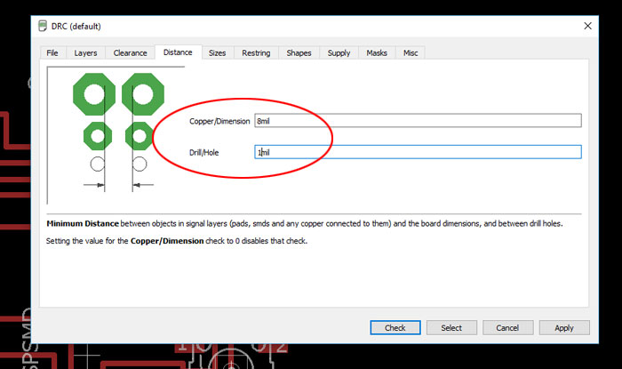
This was the numbers for the "Distance" tap.
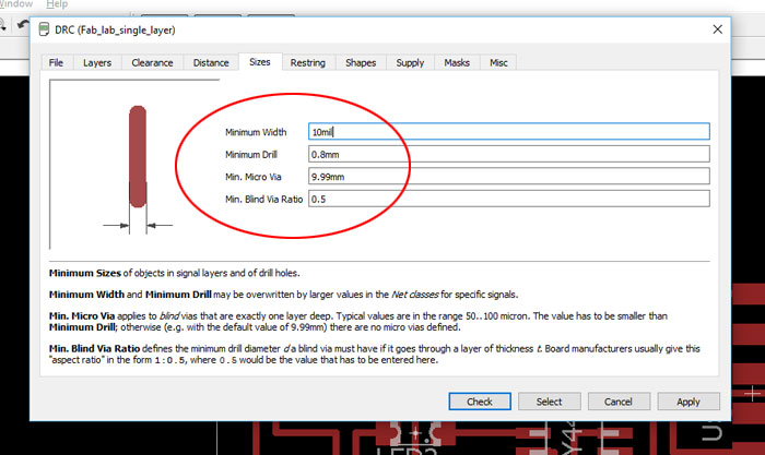
Finally this was the setting for the "Size" tap.
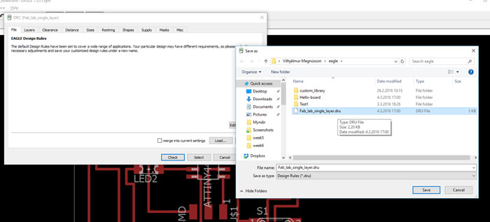
I saved these settings in my Eagle folder. Then I ran the Check and in my case everything was OK. If something is wrong with the traces this check will show where it is and you need to respond to that.
Next step was to prepare for export and we need to export two PNG Images. I moved all the components and the traces with "Group" button (Ctrl and right click mouse) to the lower left corner of the white line (Outline of the board).
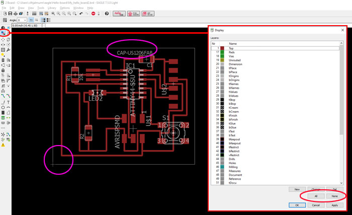
I clicked on the "layer" button and a new window appeared. There I clicked on "All" so I would open all layers. The purpose was to see if any text or anything is outside the boards outline. For right size of the exported PNG image we don´t want that so if anything is outside the white line we need to delete it.
If any names are sticking out of the white box use the Smash button to delete it.
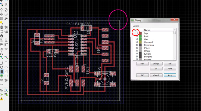
I went to layers again and turned off all layers by clicking on "None" button. Then I activated layer number "208" layer by clicking on that number in front of the layer's color. Then I went to the canvas and drew a rectangle outside of the board outline. This new rectangle on layer 208 will help us to make the PNG Cut-Out picture for the board.
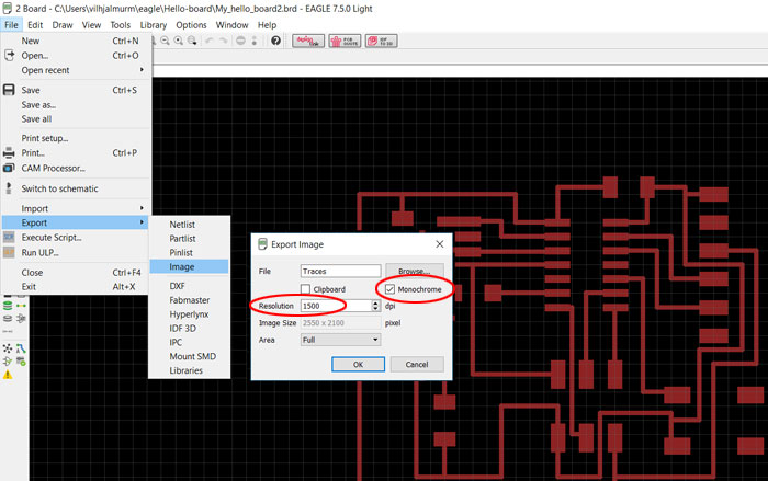
Next I activated only the "Top" layer and on that point I was ready for the export of the traces. I closed the Layer window and clicked on File/Export/Image and I got this Export Image window. In that window I named the file "Traces". I set the Resolution to 1500 dpi (Very important) and clicked on Monochrome to get black and white PNG photo and hit OK.
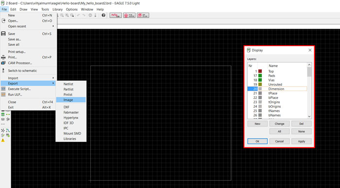
To export the Cut-Out PNG I opened the "Dimension" layer number 20 and went through the same export process above File/Export/Image. Because I made a rectangle on the layer 208 layer I got some kind of bleed of few mm. When I had made the layer I turn it off. Some people also extort that layer as a PGN and combines 208 PNG and Dimension PNG in some photo editing software. But I only extorted the Dimension layer as a PNG and opened it in Photo Shop to fix it (Fill white color inside black frame).
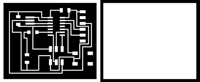
Two PNG images ready for Fab Modules.
Milling the board
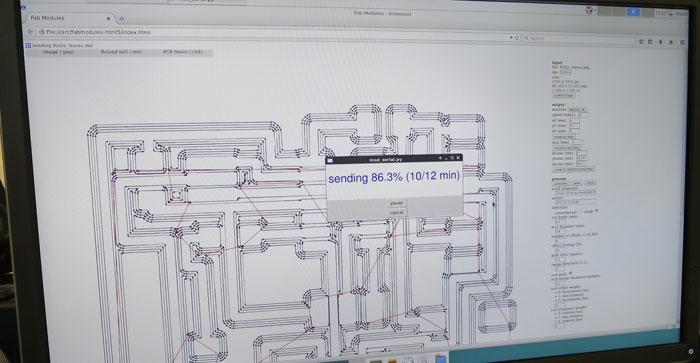
The process for milling the traces and cutting out the PCB board was the same as in Week 4 .
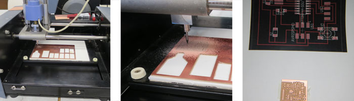
After cutting the board I saw that the traces were not centered. I have to take a better look how I export the PNG files, something wrong there. The board is usable though it´s just a matter of look. Later I found out that I did a mistake exporting the trace PNG file. As you can see there is a white space around the traces (picture above), that white space should not be there.
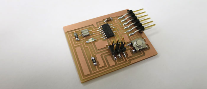
The hello World baord ready for programming!
Related links
Tutorials for Eagle - Schematic DesignGood Fab Academy Electronic Design Documenting
FabLab Electronics