
WEEK 6 / Mar 01
Electronics design
The assignment
This week’s assignment was to draw the board and add a LED (with current-limiting resistor). We were required to check the design rules, make it and test it.
Copy the Libraries

%20080337.jpg?crc=3906944052)
I then proceeded by importing the libraries of components from the lecture, mylibrary.lbr .
%20080456.jpg?crc=187335242)
Create new project
We’ll start by making a new project folder for our design. In the control panel, under the “eagle” tree, right click on the directory where you want the project to live (by default EAGLE creates an “eagle” directory in your home folder), and select “New Project”.
Here I cleaned the PCB with water.
%20080828.jpg?crc=446132928)
Create a Schematic
The project folder will house both our schematic and board design files. To begin the design process, we need to lay out a schematic.
To add a schematic to a project folder, right-click the folder, hover over “New” and select “Schematic”.
A new, blank window should immediately pop up.
Adding the Components
The ADD tool (on the left toolbar, or under the Edit menu) – is what you’ll use to place every single component on the schematic. The ADD tool opens up a library navigator, where you can expand specific libraries and look at the parts it holds. With a part selected on the left side, the view on the right half should update to show both the schematic symbol of the part and its package. The ADD tool also has search functionality – very helpful when you have to navigate through dozens of libraries to find a part. The search is very literal, so don’t misspell stuff! You can add wildcards to your search by placing an asterisk (*) before and/or after your search term.
%20081026.jpg?crc=140137252)
Next we’ll add four different parts. Use the add tool for these parts:
- ATTINY84
- Resistors
- Led
- Peripherals
- Power inputs
%20081140.jpg?crc=174104442)
Wiring Up the Schematic
With all of the parts added to our schematic, to wire them together. There’s one major caveat here before we start: even though we’re wiring parts on the schematic, to connect them together.
Instead, we’ll use the NET tool (left toolbar, or under the Draw menu). The WIRE tool would be better-named as a line-drawing tool, NET does a better job of connecting components.
%20081213.jpg?crc=4203977627)
Create a Board From Schematic
To switch from the schematic editor to the related board, simply click the Generate/Switch to Board command – (on the top toolbar, or under the File menu) – which should prompt a new, board editor window to open. All of the parts you added from the schematic should be there, stacked on top of each other, ready to be placed and routed.
%20081352.jpg?crc=4011942580)
Routing the Board
Routing is the most fun part of this entire process. It was turned each of those gold airwires into top or bottom copper traces.
%20081512.jpg?crc=382203807)
To draw all of our copper traces, I used the ROUTE tool. After selecting the tool, there are a few options to consider like: layer, width, bend style.
Checking for Errors
Before we package the design up and send it off to the fabrication, there are a few tools we can use to check our design for errors.
%20081605.jpg?crc=287783310)
Converting the PDF files.
this video shows how to prepare the files to use Adobe Illustrator and generate aPDF file and vector.
Laser Engraving
My friend Eduardo who is also taking the Fab Academy had the idea to dye the PCB board with black spray paint.
then we placed the board in an optical fiber CO2 laser engraver to reveal the traces needed for the circuit as shown in the video.
%20081958.jpg?crc=526965233)
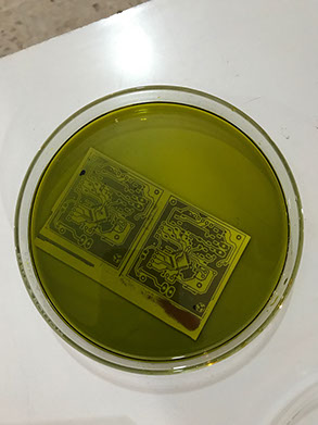
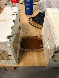
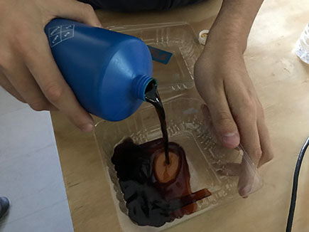
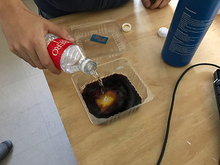
Chemical Abrasion
this picture shows how the PCB is introduced in ferric chloride, this chemical reacts with the copper layer that is not covered by the paint and eliminates it.
For this chemical one need to mix 2 parts of ferric chloride and one part of water in a plastic reservoir and introduce the PCB until the copper is gone.
The we clean the the PCB with paint thinner to eliminate the black paint.
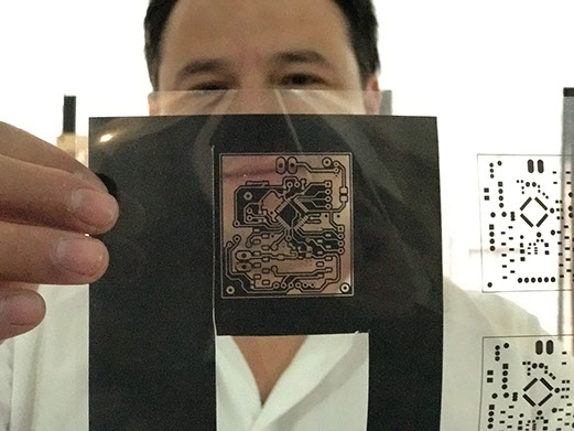
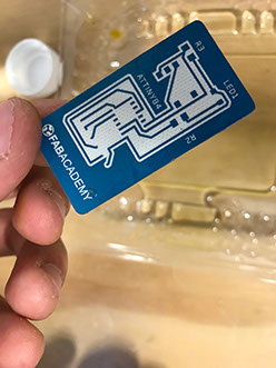
Electronics Design for Final project
I repeated the previous steps to design the PCBs for the final project.
Final Project
Create new project, Create a Schematic, Adding the Components
Create a Board From Schematic, Routing the Board, Checking for Errors
%20084108.jpg?crc=4191371153)
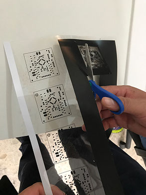
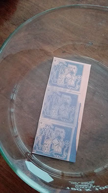
Chemical Abrasion
So I learned a new technique for fabricating the boards using film.
%20080930.jpg?crc=349484016)
%20081630.jpg?crc=430724995)
%20082722.jpg?crc=4014455396)
%20083059.jpg?crc=321623161)
%20084755.jpg?crc=93922118)
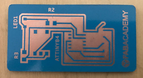
The final board
%20084252.jpg?crc=4213506865)
Oscar Velázquez