Eagle software
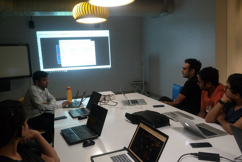
We started this week by a session on Eagle by one of my office colleague Mr. Ayush Jain
Takeaways from the session and important point regarding Eagle software

If we are using any new component and it is not available in existing Eagle library same has to be created which is a time consuming job.
For this I use www.snapeda.com. Millions of components libraries are available for free on this site.

For my final project I had to use LM 3S 6965 whose library was not available I downloaded it from snapeda.com.
Click here to go to Snapeda.comIf you wish to download any component library from Snapeda.com. You have to follow below steps.
Before proceding this site asks you to register. Once you sign up using your valid email id you can access the resources available on site.

Using the search option search for desired part. In my case it was LM 3S6965


Select your desired part from the list

Then click on download footprint and symbol.

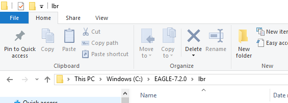
Once the library file for desired part is downloaded save it in eagle library folder.

Then the library will be visible in list of libraries.

For using the component we have to activate the library. A green dot come in front of library

Selecting the components

Making Hello world schematic using eagle
- As Eagle was already installed on my laptop there was no requirement for me to download it. But those how are new to Eagle can download it from below link. Click here to go to Eagle download page.
- Next step is to add FAB library and save it in Eagle library folder
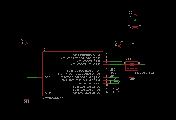
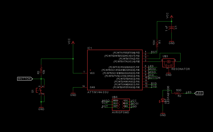
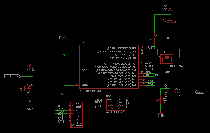
- Refering Hello world circuit diagram started making the circuit diagram
- Add ATtiny44 IC and give label to its pins. Add resonator, VCC and Ground. Out of the free pins I decided to use PA7 for LED and PA3 for button
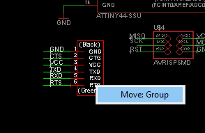
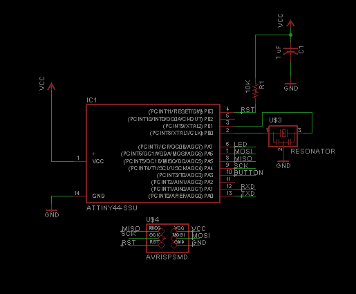
- Step 2 was to add programming connector. And giving label to its PINs
- Then added LED along with current limiting resistor and button.
- Add finally seial connector for communicating with PC
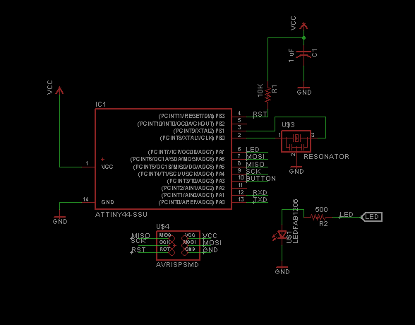
Now the schematic is ready and now we required to prepare the board file
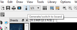
Now click on switch to board. Now you will move to layout mode. All component selected by us will be shown on left bottom corner of the screen.
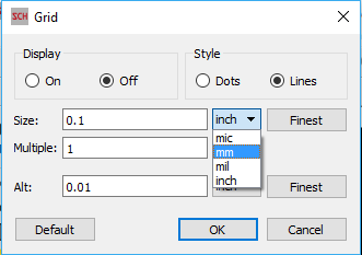
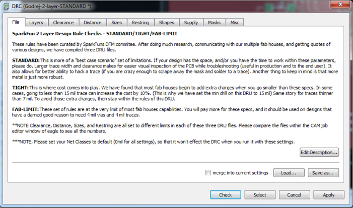
Next step is to enter DRC value, For manufacture PCB on milling machine we need to take care of clearances. For example if milling bit is of size 0.5mm then traces should be defined with atleast 0.5mm clerance. Otherwise we may end up with very thin traces or else sometimes traces will vanish. Design rules can be set in eagle cad under menu Tools > DRC for proper milling it is required to have track width and clearance of 0.5mm.
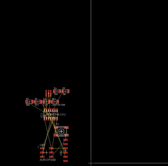
Manually placed the component at appropriate places, on selecting the component use right key to rotate them.
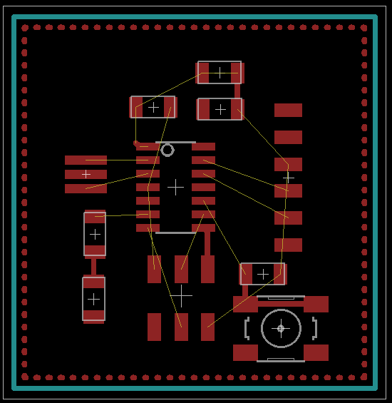
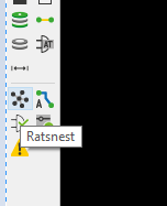
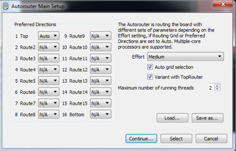
Now we can do autorouter function of Eagle
Else manually route the components. Yellow line shows the connections to be made. Also I have added ground polygon.
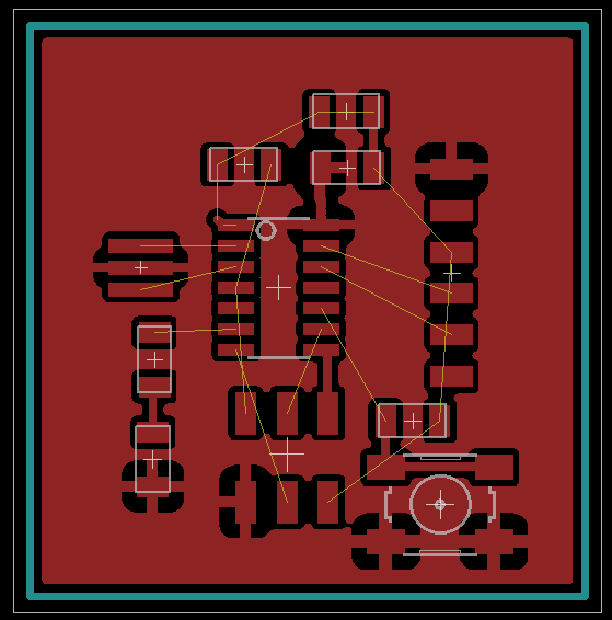
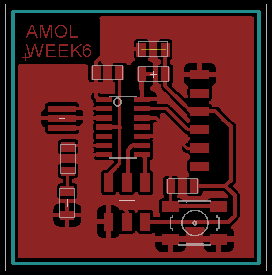
Have given name to each board for easy identification. Add name to the copper layer for it to get printed on PCB.

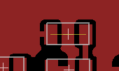
After placing all component layout looks as below
If one is not able route the track as they are ovelapping, can use o ohm as shown below
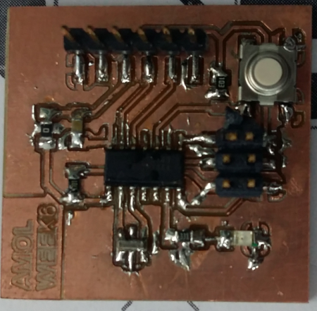
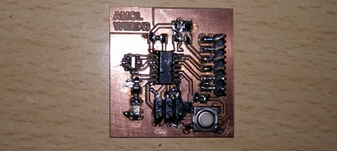
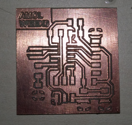
Once layout is complete export the file as png and go ahead with milling. After milling is completed PCB look as below:
Task 1 is to stuff the microcontroller and crstal.
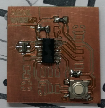
Then proceed with stuffing all the remaining components. Final PCB looks as below