
This week assignments are:
- redraw the echo hello-world board
- add (at least) a button and LED (with current-limiting resistor)
- check the design rules, and make it
- extra credit: simulate its operation
We got an introduction on how to use Eagle in our classes. Eagle is a flexible electronic design automation application with schematic and printed circuit board (PCB) layout editor. For the schematic is very similar to other software that I used before as Cadence and Multisim, but it does not have simulation. A good thing about it, is its capabilities of PCB layout editor.
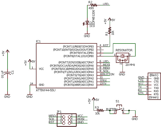
I followed the tutorial of Introduction to Eagle" but instead of download the Hello Echo schematic and board files, I started it from scratch, adding each component again.
To add the components you will need the "fab" and the "supply" libraries. The "fab" library can be downloaded here. The "supply library is already standard on the Eagle software.
To add a new library of Eagle on Windows, you will need to go to the Eagle installation folder on your computer, and find the folder lbr. In my case is C:\EAGLE-7.3.0\lbr. I changed the name of this both libraries, adding "01" before the file name, to make it easier to find while using the software.
One good thing about the Eagle is that you can always type the command you want instead of clicking on the icons. So type "add" and look for the listed components. Here the components I used:
| Part | Value | Device | Package |
| C1 | 01 uF | CAP-US1206FAB | C1206FAB |
| IC1 | ATTINY44-SSU | ATTINY44-SSU | SOIC14 |
| JP1 | PINHD-2X3-SMD | 2X03SMD | |
| JP2 | FTDI-SMD-HEADER | FTDI-SMD-HEADER | 1X06SMD |
| LED | LEDFAB1206 | LEDFAB1206 | LED1206FAB |
| R1 | 10k | RES-US1206FAB | R1206FAB |
| R2 | 499 | RES-US1206FAB | R1206FAB |
| R3 | 10k | RES-US1206FAB | R1206FA |
| RESONATOR | 20 MHz | RESONATOR | EFOB |
| S1 | 6MM_SWITCH | 6MM_SWITCH | 6MM_SWITCH |
Besides these, I also added the VCC 5V and GND from the supply library. After placing all components, I stated to connect them. I made some copies of GND and VCC to connect the different parts of the circuit. Following the tutorial, I named and labeled the nets to the schematic looks cleaner.
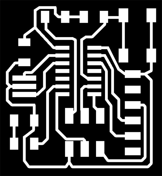
After connect all the components, I switched to board and could see all the unrouted paths (usually in yellows color). If you do not see it, go to "Layers" and select "Unrouted". Use the "Move" tool to position your components. After that try to route your connections using the tool "Route". You need to figure out how to connect them all without crossing paths to other connections.
Besides the routing process itself, my first challenge to put the routes on the positons that I wanted. I realized that the routes was snapping to some points and this makes it difficult to make the routes as I wanted, such as trace more than one route in the space between the microcontroller. At first I thought it was a limitation of the free version of Eagle, but after try to change this clicking in several icons, I found the "Grid" icon (you can always type "Grid" and a window will open). The size of my grid was too big, so that is why it was snapping just in some places. I changed it to 0.005 in and it worked.
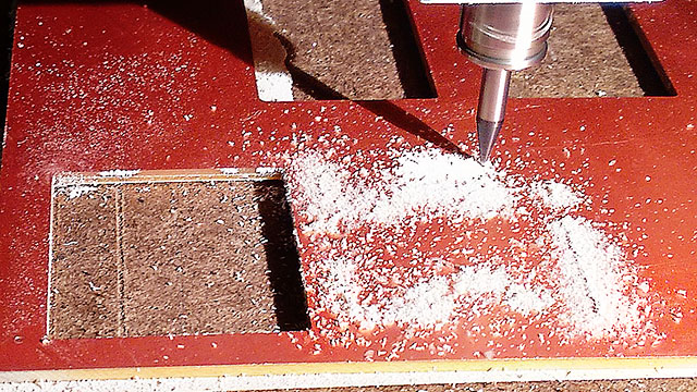
So after make all the routes as I wanted, I finally finished and exported the images to mill on the Modela. Here how's the first attempt looks like:
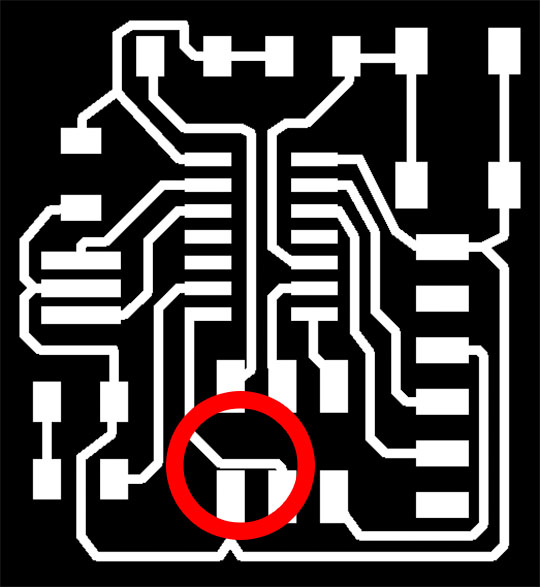
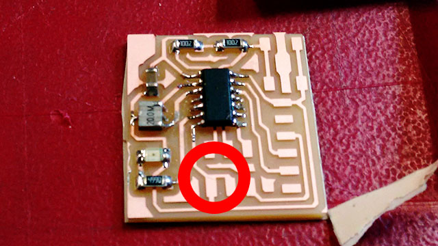
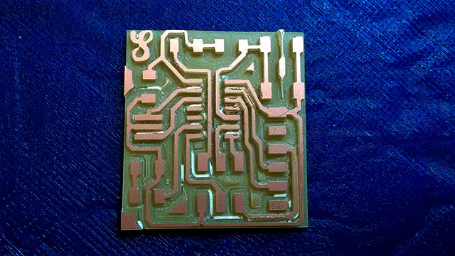
I was quite excited of make it, so I went straight to mill it on the modela. I milled it, cleaned it, started to stuffed it soldering the components, and when I was in the last component (6x2 header) I noticed that my design has an error! The route coming out from de middle bottom pin of this header was too close to the left bottom pin, so they was connected to each other and was not supposed to. That is the importance of the DRC test, which I forgot to make. Below the error in the traces and in the board.
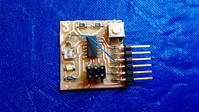
The next day I started it over fixed the error and milled a new board. It the first board I milled I had some trouble, because the double taped I used on the day before was losing the glue and taking off, so while milling the traces the board bended up a bit and made deep traces on the board (pics below). I took off the board, applied a new double tape and start over. Now it was supposed to be ok. Then I stuffed the board again soldering all the components on the board.
On the next class rechecking my board, I noticed that it still wrong. There was a missing route to the VCC from the 6x2 header, and another one connecting to the Reset Button. It happened I think because on the schematic I copied the VCC to connect in other wire. It worked for the GND but not to the VCC. I also could not name all the VCCs to the same name, so I think it created one different net for each VCC I created. For the reset button because I did not changed the name of the wire to be connected at "RST". So I changed my schematic having just one VCC +5V and changed the name of the nets, which needs to be connected to it to VCC as well, and now it worked well. Therefore, instead of making a new board, I fixed it using a wire as a jumper in the board that I already made, and making a iron soldering jump to the RST pin. It makes the board looks a bit ugly but it worked. Here how’s it looks like finished.
Even not milling another board, I corrected the schematic and the routes on Eagle. Below you can find the source files of the schematic on eagle, the PNG images for download.
Schematic: helloworldsiron.sch
Traces: traces3.png
Interior: interior.png