WEEK 6
ELECTRONIC DESIGN
ASSIGNMENT
- Redraw the echo hello-world board, add (at least) a button and LED (with current-limiting resistor), check the design rules, and make it
- optional: simulate its operation. Measure its operation
Preperation
The main aim of this week is to learn about different electronic CAD softwares, identify one of them for our electronic designs then, redraw the the echo hello world board and making it. I had used Eagle and Orcad during my graduation days so i brushed up allthose things to work with it.
PCB Designing
A PCB(Printed Circuit Board) mechanically hold and electronically connects the components using conductive tracks(Copper). There are different types of pcb's starting from Single side to multi layer pcb's. Since we are using milling machines we can make maximum double side pcb's in Fab Lab. The crosssection of the single side and double side pcb's are showed below. The copper layer is used for connectons between the components. The layer below copper layer is called substrate layer, substrate is made using fiberglass-epoxy laminates,Teflon,ceramics etc. We are using a pcb with FR (Flame Retardant), a fiberglass-epoxy laminate. In multi layer Pcb's multi layers of FR is laminated togather. There are different grades of FR; FR1,FR2,FR,FR4 etc. To know more Click here
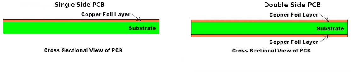
PCB cross section
Flame Retardent 1 (FR1)
PCB Substrates are specialized materials that do not conduct electric currents. They serve as a laminated electrical insulator between circuitry, An electrical insulator is a material whose internal Electric charge do not flow freely, and which therefore does not conduct under the influence of an each layer of circuitry, consequently, is connected through plated through holes to connect traces on opposite layers. FR-1 is a hard, flat material that consists of a thin layer of copper over a non-conductive phenolic paper copper-clad. FR-1 is primarily used for making circuit boards. The thin copper layer can be milled or etched away, leaving traces to which electronic components can be soldered. Substrates requires electrical,mechanical,and thermal properties. I have gone through some documentation on different pcb's and if any body interested can go through this link
Is FR-1 safe?
Unlike FR-4, which is fiberglass-based and generates dangerous glass-shard dust when milled, FR-1 is safe to use if you keep it away from your eyes, lungs, and skin. It is recommended vacuuming up the debris after the milling. Typically specified to 105 °C, some grades rated to 130 °C. Poor moisture resistance, low arc resistance are some features of the FR1 material.
PCB Design
PCB design is usually done by converting our circuit’s schematic diagram into a PCB layout using PCB layout softwares. There are a lot of open source software packages for PCB layout creation and design is available now, both open source and licensed. In this week i am planning to familiarise with these softwares.
PCB design and layout process
The first process of PCB design starts with circuit schematic design, using any one of the softwares we can design the circuits. Each software will have a schematic design tool for this. We can draw our circuit schematic by pick and placing the components available in the library, interconnect it using wires. Once completed the schematic the next process is routing of pcb, the PCB software routes the physical connections on the board according to the netlist from the schematic. To achieve this it will use the number of layers that are available for connections, creating via holes as required, but in our case maximum double layers is only possible with the pcb modela milling machine . Autorouting and manual routing provisions will be available in softwares, also we can check the design rules at different stages. After completing the routing we can use the output to make the pcb,noramally most softwares the output will be in the form of Gerber files. It is an open ASCII vector format for 2D binary images. It is the standard used by printed circuit board (PCB) industry software to describe the printed circuit board images: copper layers, solder mask, legend, etc. Since we are using mechanical etching the output required will be in the form of images(.png).
Eagle CAD
Easily Applicable Graphical Layout Editor (EAGLE) is a software application that makes it possible to design electronic circuit boards(PCB) developed by CadSoft Computer GmbH and now acquired by Autodesk Inc. There are Premium, Standard, free, and student & educator editions.
Installing Eagle
There are different versions available in internet. I followed this documentation to install Eagle 7.3 in my pc. There is one latest version is also available Eagle 8.0.2, i opted free licensed version and registerd using my Autodesk account. It was installed correctly
Work flow of Eagle
1. Add the components from the Library
2. Draw Schematic of desired circuit
3. Arrange and route the Board
4. Check for Design rules and ERC errors
5. Give proper border and export as PNG file
Some usefull tutorials for learning about Eagle is given below:
Link 1: Video Tutorials
Link2: Sparkfun documentation
Designing Echo hello world board
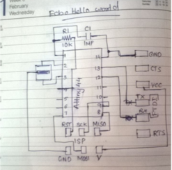
This week main assignment is to redraw echo hellow world borad with some extra componenets. The board schematic was downloaded from the class archieves and i transfered the schematic in my diary.
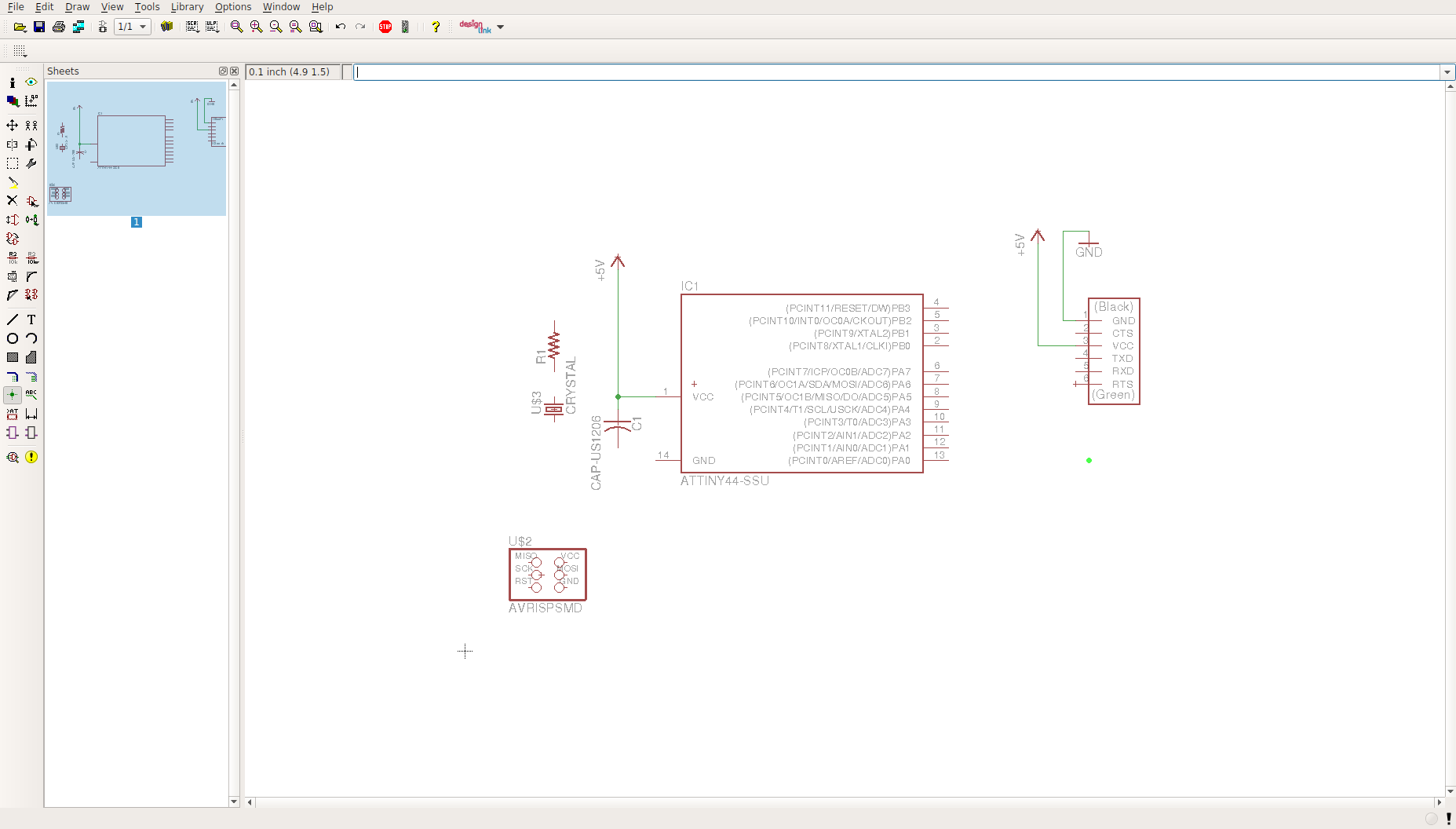
Echo hello world board is a Attiny44 based board, have gone through the Attiny44 data sheet, made an idea about the pin configurations and features. Next opened eagle software and created a new project and inside it craeted a new schematic with the file name "echo hello world". In the schematic window place components from the library. There is default fab library available in archieves for eagle :fab.lbr, I downloaded it and added to the library. Placed the components from the fab library in to the schematic, the schematic requires the following components.
| 1. ATtiny44-SSU |
| 2. 20mhz resonator |
| 3. Resistor-10K |
| 4. Capacitor-1uF |
| 5. AVR ISP Header SMD |
| 6. FTDI Header |
| 7. Capacitor-0.1UF |
| 8. Switch Omron 6mm |
| 9. LED SMD |
| 10. Resistor-499Ohm |
Extra i have added VCC and GND(ground) labels in the schematic; this is one of the easiest way to draw schematics. We can add labels instead connecting wires or nets. The nets with same label will automatically get connected.
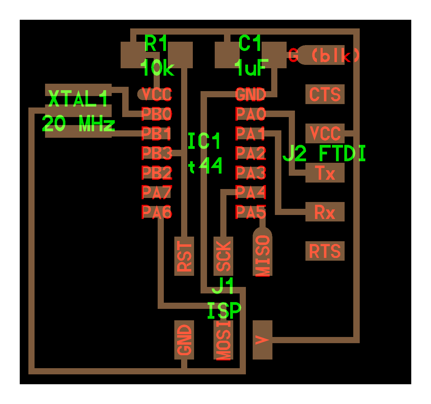
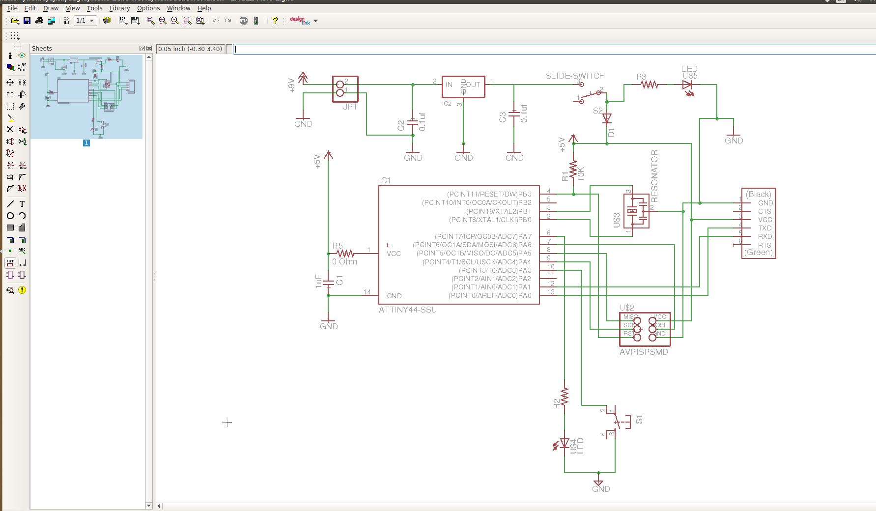
Completed the schematic of echo hello board, added the switch to port PA3(pin no:10) of the Attiny44 along with a LED and Resisitor to PA7(pin no:6). The schematic screen shot is given below
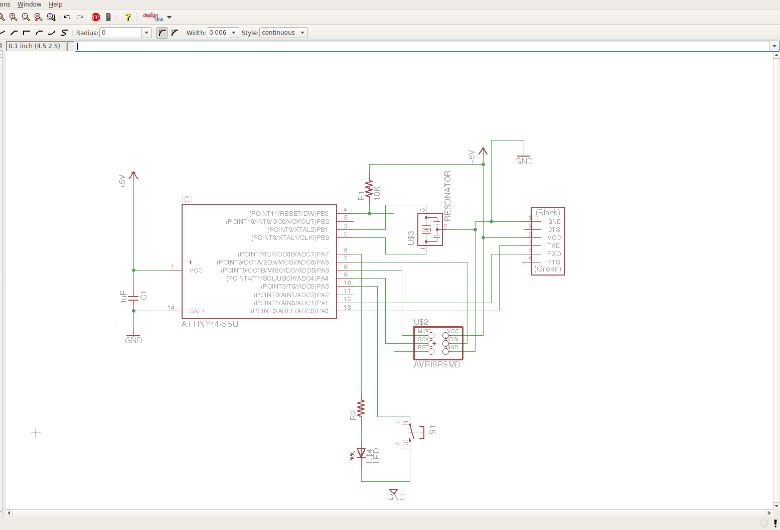
Battery Operated Echo hello world
This circuit is intended to control a LED with a switch, when the switch is pressed the LED will glow. The echo hellow world board always require a usb cable to power the circuit. So i thought of making it a stand alone board working in battery, for that i designed and added a volatge regulator circuit with a control switch.
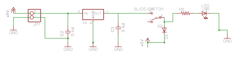
This section is controlled via a slide switch,a voltage regulator of 5V with 100mA current rating and a LED indicator to identify the mode of operation. It's having two modes
Normal mode and Battery mode. When using the cables for programming there is no need of extra supply to power the board, In such situations we can turn OFF the Voltage requlator by moving the switch to OFF position (Normal position).
this mode is called "Normal mode" . After programming the board, We can switch to battery operating mode by changing the switch position to ON position, this is called "Battery mode". Now the board will get power from the battery through the dide D1, D1 also
protects the voltage regulator circuit while the board is in Normal mode, otherwise reverse voltage from the USB will go into the output of regulator and will damage the device sometimes, In
such situations the D1 diode will be reverse biased and ensures so no power will go into the regulator circuit. Once the board is programmed to control the LED, We can connect a battery of 9V through the Jumper J1. This is the final schematic of my echo hello world pcb.
Electrical rule check (ERC)
It involves checking a design for all electrical connections in our designs. It will shows errors, warnings etc, we can check this and correct the errors from
the schematic. We can look each errors individualy and it will be pointed in the schematic . After ERC checks, Next step is the routing of Pcb , for that we can switch from schematics to borad using "Generate/switch to board" button from the tool bar. This will show like the picture
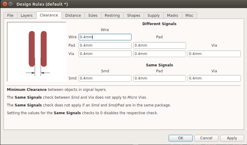
attached below. First before doing routing we have to set the design rules, the design rules are the most important thing relates to the traces width, clearence between the traces etc and is the most important thing while designing pcb's for
mechanical etching.
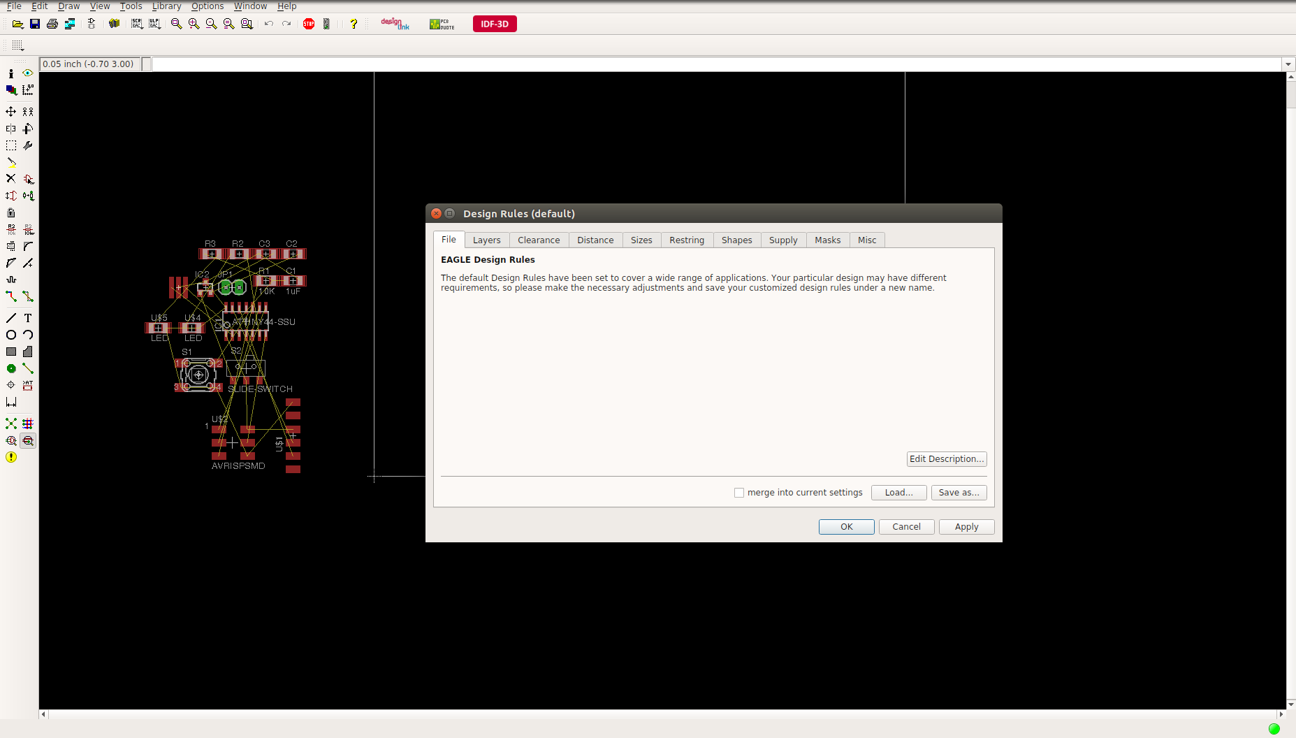
This is clearence i have given for routing, 0.4mm is our bit diamension so every thing is set to 0.4mm (equivalent to 1/64 mils)
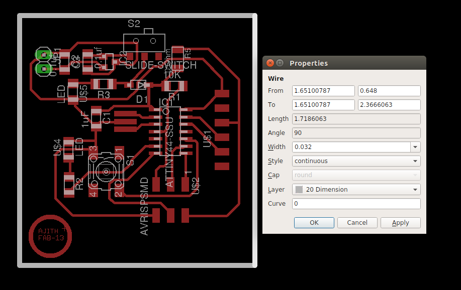
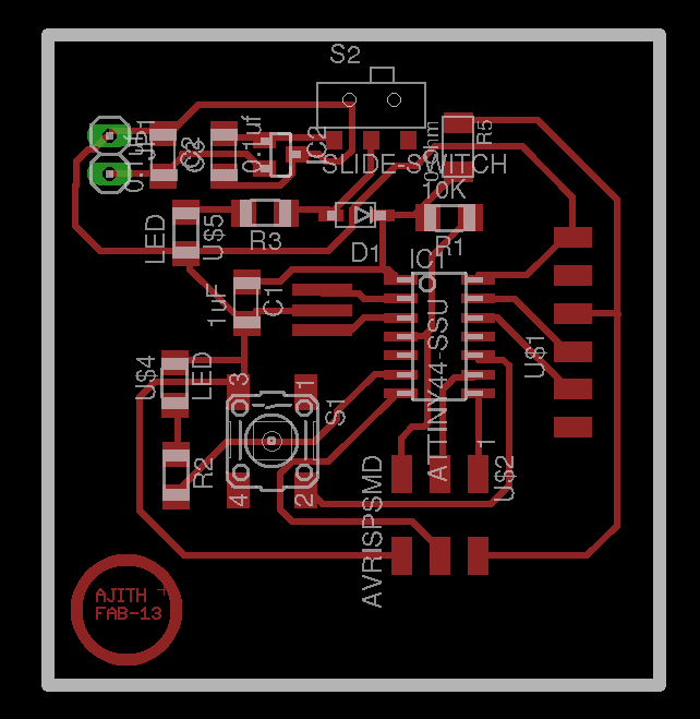
Next placed the components inside the dimension boundary according to the interconnections, this is a tricky part because better arrangement gives better routing. I placed the componenets and routed using the manual routing tool, ensure all routing are done in the top layer . I confirmed everything is correct and finalised my pcb routing. Added a circle with my name and fab 13 as text. After this we have to set the dimension for the boundary for cutting out the board. Moved the box according to my board size using mouse and changed the dimension to "0.032 inch" (equivalent to 1/32mils) to cut the board with 0.8mm bit. The picture shown below is my final echo hellow world board layout.
This is my echo hello world board
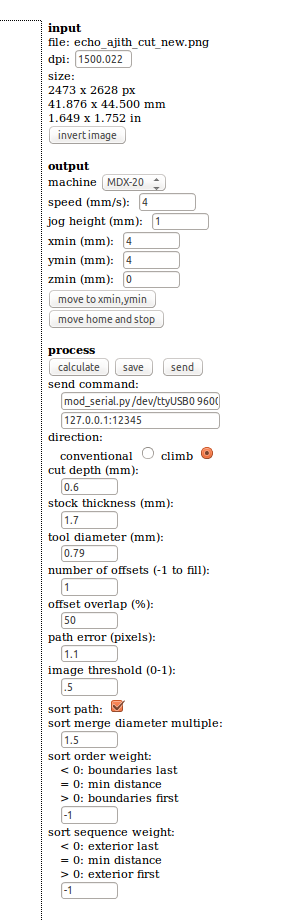
Files for Milling and Cutting
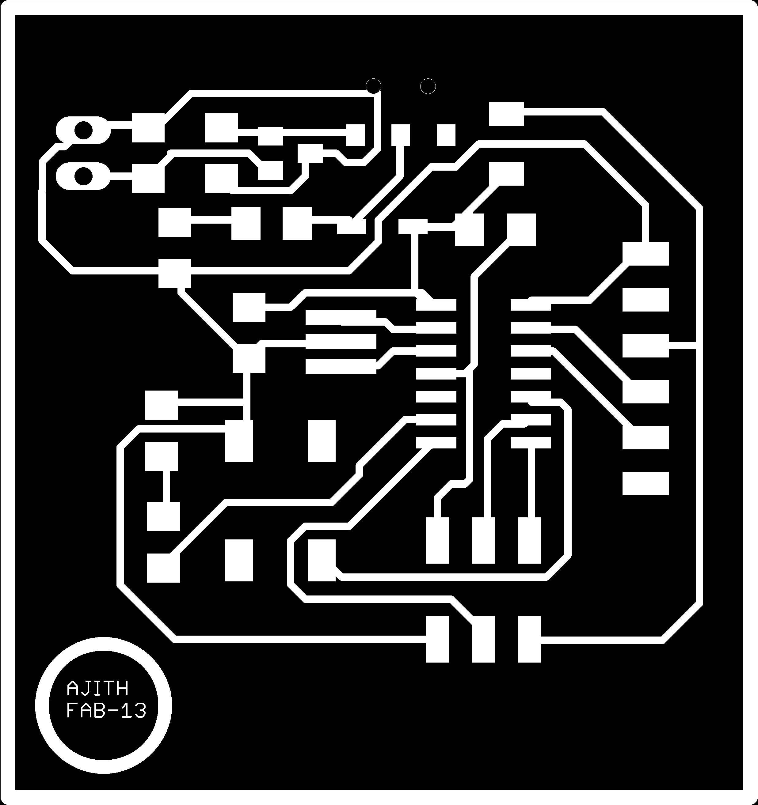
To process the board with modela we require two files(images) with ".png" extension one is for Milling the traces and another for cutting the board. The routed bord is to be exported to .png format from the file menu after selecting top layer, pads, dimension from the layer menu bar for cutting the board selectthe dimension and drill holes(for fixing the jumper J1) and export to .png format. Both of them were exported in monochromatic format with a dpi of 1500px and saved to my folder. For cutting we have to invert the color of the image . The exprted milling trcaes and cut traces images are shown below.

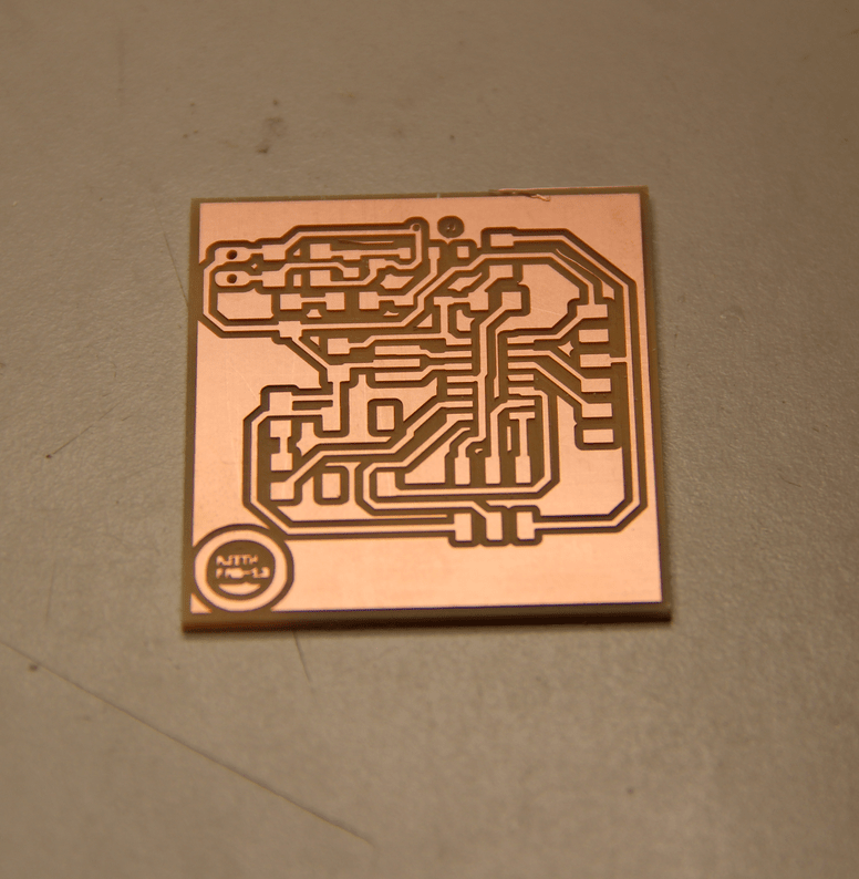
Milling of Pcb
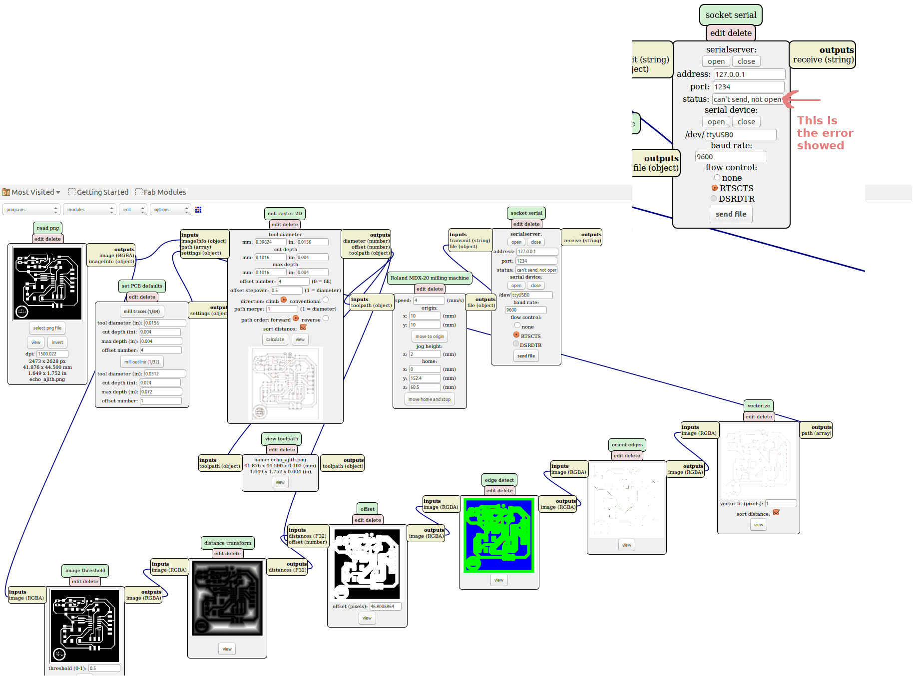
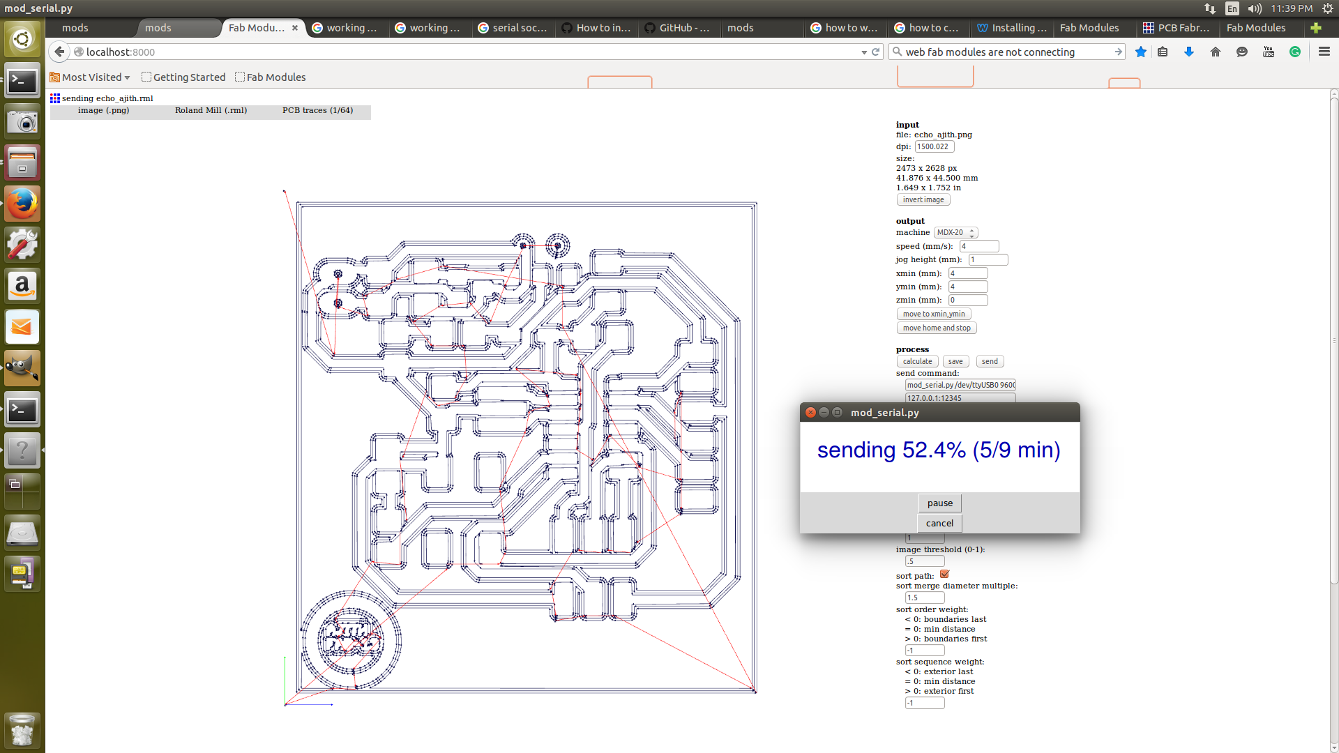
The first step of milling is setting up modela, the detailed documentation for the setup is is there in my Electronics production week. For milling the pcb we are currently using the old compiled version of the fab modules. This week i tried the latest webwersion of fabmodule called mods In neils lecture he explained the working of it, I followed the lecture and opened my mill traces file in mods setted the bits and other parameters perfectly but it didn't connected to our machine"Modela CNC", we have tried with different port address and tried with other flow controls but it didnt got connected. Our instructors told that we need some cable to work with modela in mods. The screen shots are attached below.
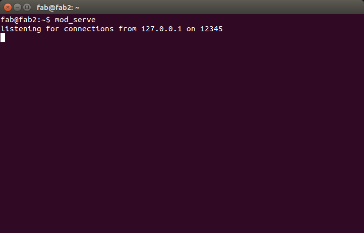
Next we thought to do the same process with the current version of Fabmodules web version called fabmodules-html5 , then our instructor Mr. Vishnu told that they have tried the webversion lastyear and is working but in between the machine is behaving irratically, So we planned to move to the offline webversion ,which can access locally. gone to the github documentation, followed the installation steps from this link GitHub. Everything is installed and to start the operation i did the steps as shown below.
Steps to start fabmodules
Step1
#Type the code below in terminal
command - mod_serve to start node server
Step2
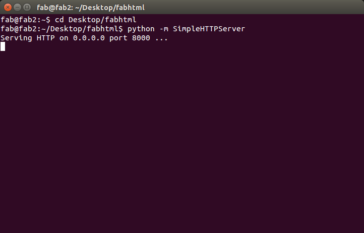
#keep the above terminal open
#open another teminal, navigate to directory for  webmodulesHTML-master(fabhtml) and type
cd Desktop/fabhtml
#Type
python -m SimpleHTTPServer
Step3
Open firefox browser
localhost:8000
#Ensure both terminals are opened and working correctly
The steps i did is shared below as screen shorts.
Once we opened offline webmodule by typing "localhost:8000"in web browser, We will be directed to the offline version page similar to the online web version.
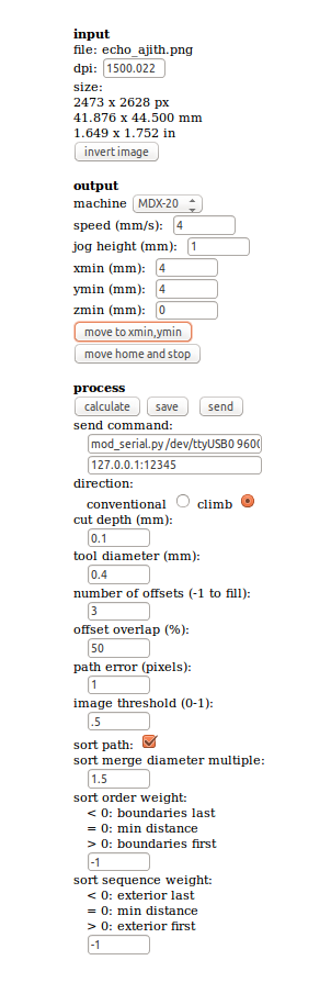
Then select the process and set other parameters such as bits, X,Y,Z axis and offsets etc and is showed in the screenshot.
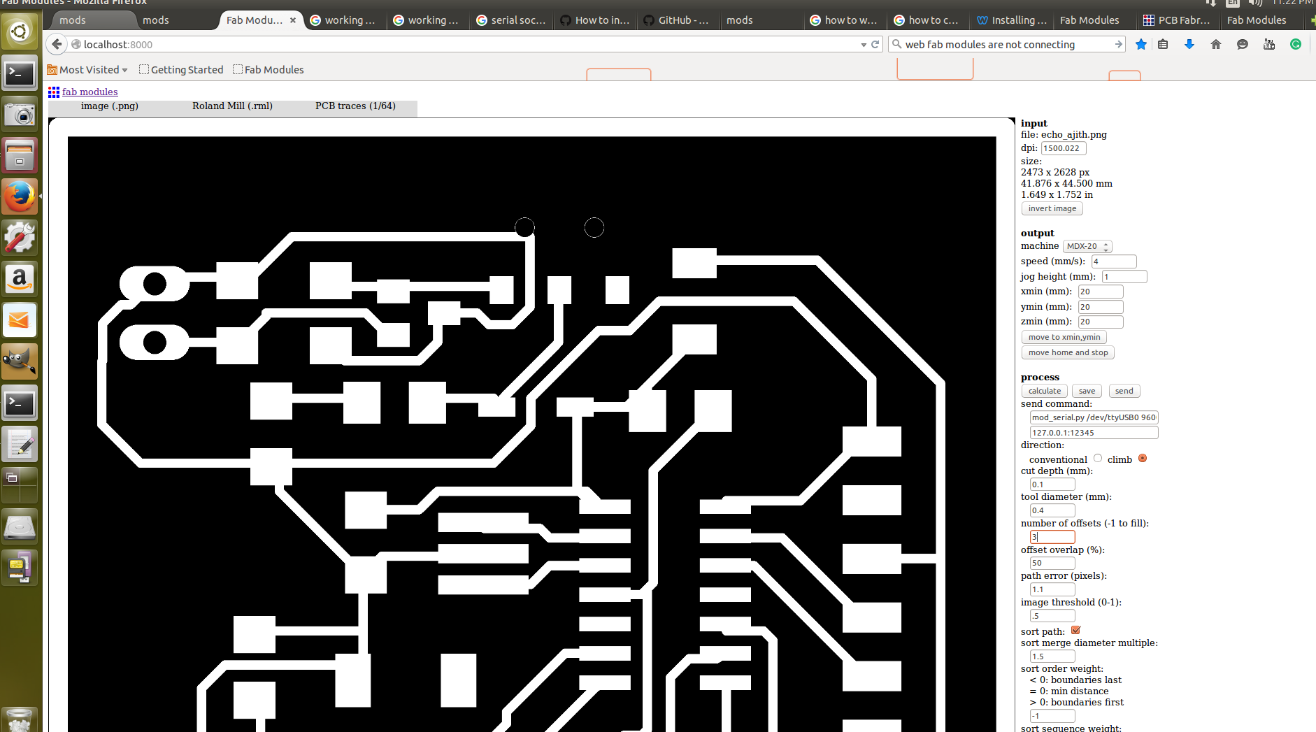
The final panel settings i given is showed below, after setting all the parameters, Moved to the machine there 1/64mil (0.4mm) bits were put for milling and fixed the Z zero and started the work. The screen shot below shows the process flow at 50%.
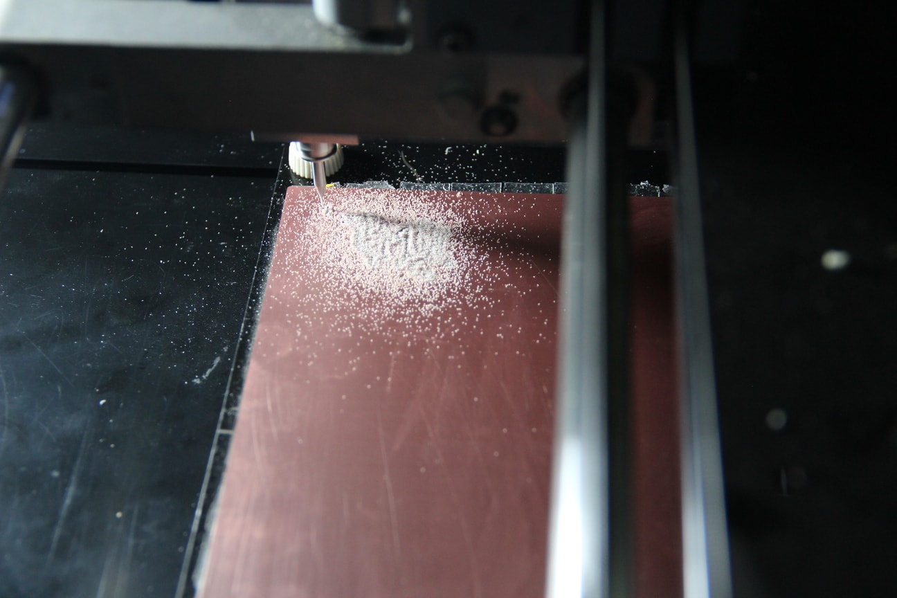
Cutting the Pcb
I followed the above steps, changed the image to cut part image, bit is changed to 1/32mil (0.8mm) and other parameters as shown below and started the process.
The final settings i have given for cutting my pcb is showed below.
This is my milled echo hellow world PCB
Design of Current limiting resistor
To find out the resistor required for the Blue LED ,as current limiting resistor ,first we have to check with the datasheet and find out the DC forword voltage and forword current, and i found it as:
LED DC Forword Voltage = 2.8V
LED DC Forword current = 20mA
Resistor value for the Blue LED can be calculated
R = (Vs - Vf) / Ifc
=> R = (5V - 2.8V) / 0.02A
=> R = 110 Ohm
Resistor value for the Red LED can be calculated ( for Battery mode indication )
LED DC Forword Voltage = 1.8V
LED DC Forword current = 20mA
R = (Vs - Vf) / Ifc
=> R = (5V - 1.8V) / 0.02A
=> R = 160 Ohm
In our lab we have standard resistor values are available like 10, 100,49.9,499 ohm etc, So i selected 499 Ohm for both the resistor, this wont effect the working of the LED but the current through each will differ and the brightness will vary.
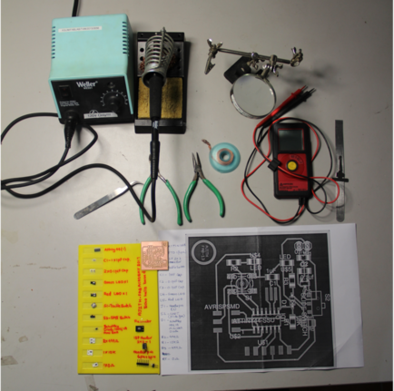
Soldering the PCB
I have collected the components from the inventory and soldered the components to the board.
| ATtiny44A SSU | 1 No |
| Resistor 10KΩ | 1 Nos |
| Resistor 499Ω | 2 Nos |
| Diode Schottky 100V SGL SOD123 | 1 No |
| LED Blue | 1 No |
| LED Red | 1 No |
| Capacitor 1UF | 1 No |
| Capacitor 0.1UF | 2 Nos |
| ISP Header 2X3 | 1 No |
| FTDI connector(6pin) | 1 No |
| Jumper pin(2pin) | 1 No |
| Switch slide SPDT 12V | 1 No |
| Switch Tactice SPST 24V | 1 No |
This is my set up for soldering the board, used weller WSD51,with other tools for soldering like solder,tweezer,nose plyer,wire cutter, solder wick and multimeter etc. I have taken a schematic copy for easy soldering, noted all the polarities and carefully soldered the board.
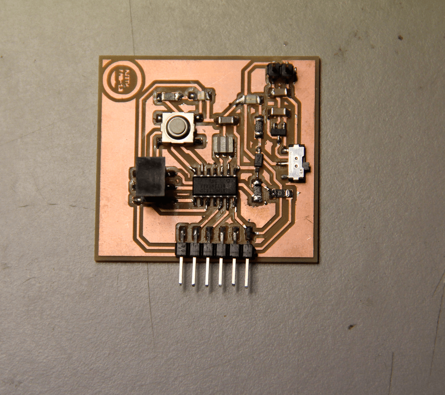
This is the hero shot of my pcb after soldering. It is better to check the continuity of the board with a multimeter. Atleast the resistance between the VCC and GND must be checked, because as it is a non masked pcb the chances of minor shortings and solder splats are more.
Testing echo hellow board
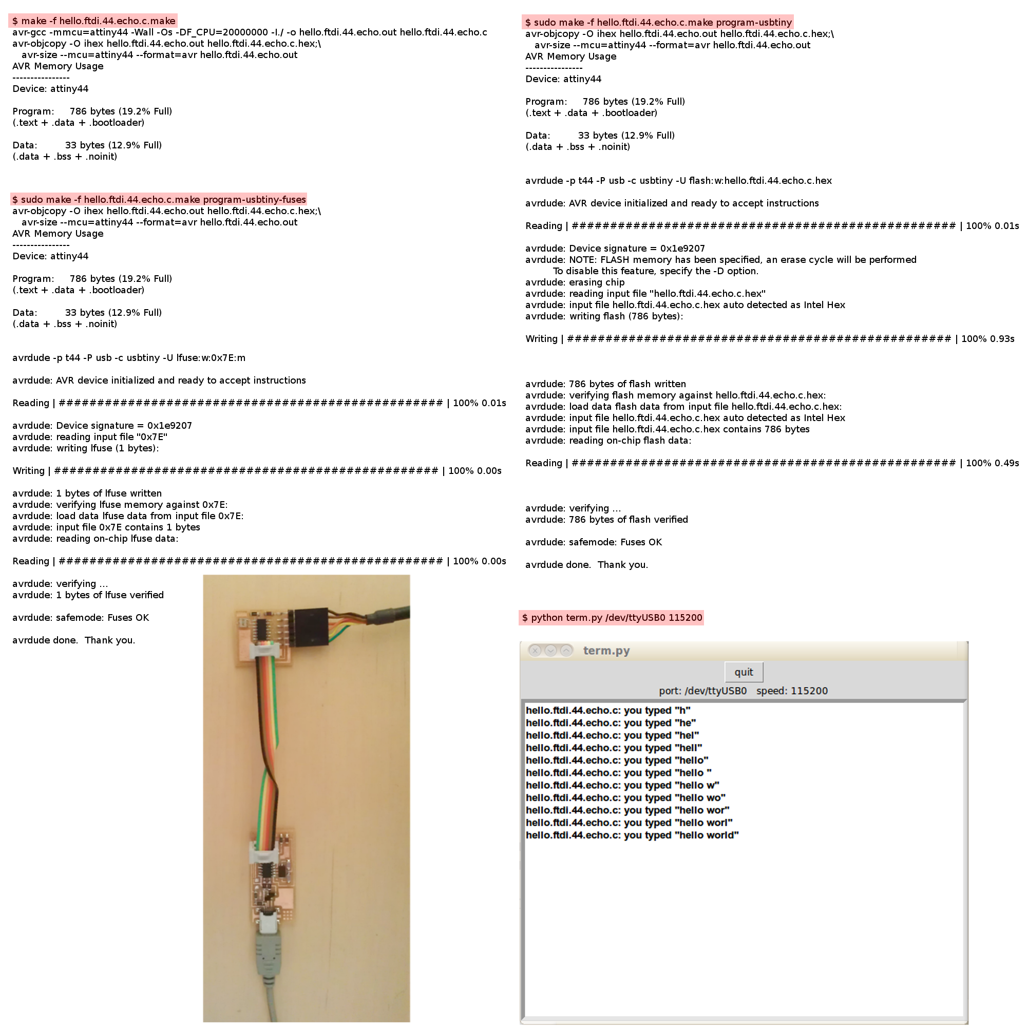
This was the last part of the assignment, after completing the soldering just cleaned the board and visually inspected for any shorts or other defects, i didn't found any faults visually. Next part is testing part, our instructor Mr.Yadu helped me to program the button program to it for checking the board, its worked and later i changed the power supply to 9V battery and that was also worked perfect. I came to know that this week we have to check the board with FTDI echo hello world program, so i have gone to the archives and followed the documentation. In order to program the board we have to download two files from the archive i.e. hello.ftdi.44.echo.c and hello.ftdi.44.echo.c.make. Saved it in a folder, Opened terminal from the folder. Connected my echo hello world through my Fab ISP board, and powered my echo board using the ISP cable, this time i noticed that my Attiny44 is getting too hot, confirmed that something is wrong in the board. Then checked in battery mode the same result i got.
Trouble shooting the board
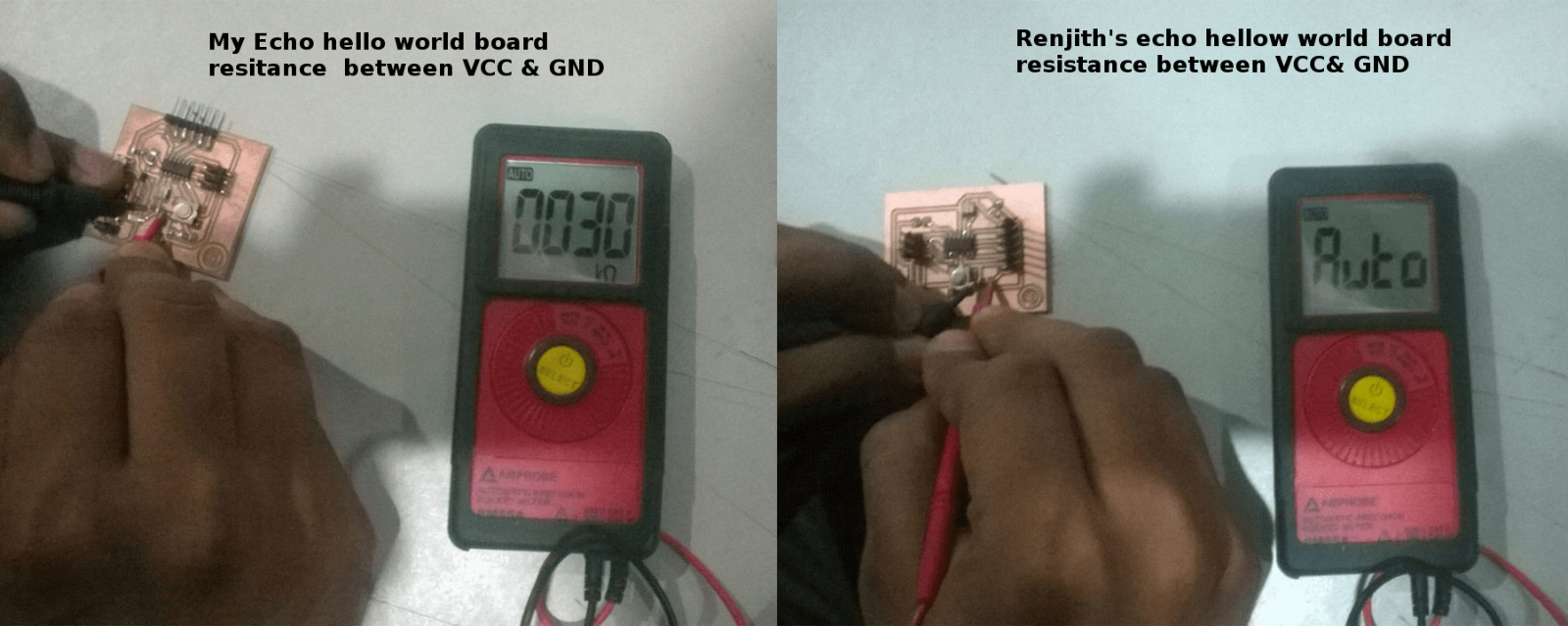
I had past experience in debugging the boards, So first i visually inspected the board and didn't find any shorts, Next i checked the resistance between VCC and GND across the 1UF capacitor and it showed "30 Ohm", i noted this is the main issue with my board, some shorting i expected in my pcb. Then i checked the same resistance in my friend Mr. Renjith's board and it showed overload(high resistance) as shown below.
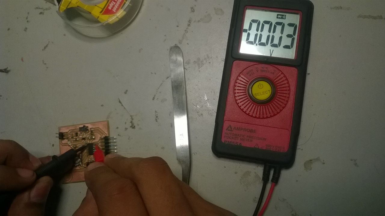
Next i have moved to work bench and using soldering iron carefully i lifted the VCC and GND pins from the pcb pads and checked the continuity, this time also it showed the same resistance as "30 Ohms". Now by this step i confirmed that my Attiny44 IC is shorted in between while testing , i don't know the exact reason behind it, may be due to some solder splatter or over current from USB.
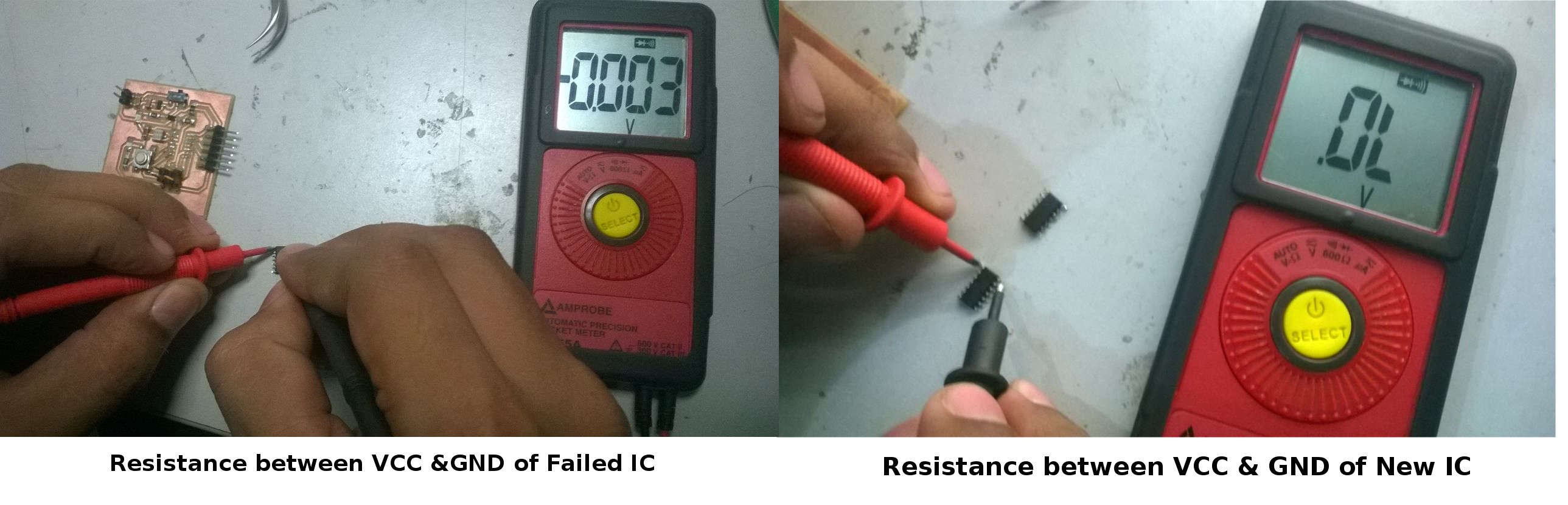
I removed the IC carefully without any pad lifting and checked the continuity once again to confrim that the problem is due to failure of IC and it showed almost short resistance as shown below, i also checked the same with anew Attiny IC and it showed "Overload(high resistance)".
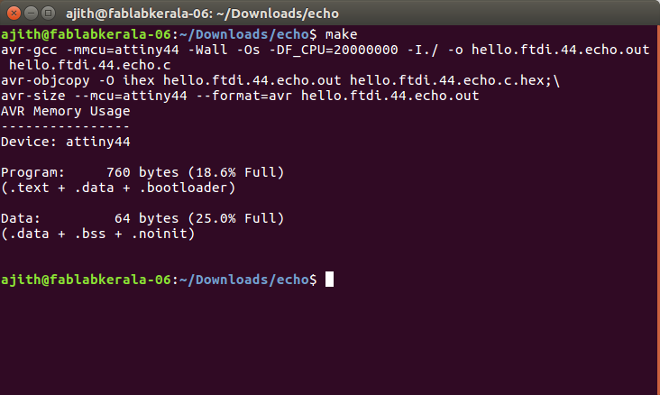
Next i cleared the pads with solder wick and the soldered the new IC and after soldering it ensured the resistance between VCC & GND as high. Then started programming it. First i downloaded the hello.ftdi.44.echo.c. Then downloaded the make file "make file" renamed it to "make" and run the following commandas in terminal from the program directory.
make
make program-usbtiny-fuses
make program-usbtiny
These are the screenshots of the programming part

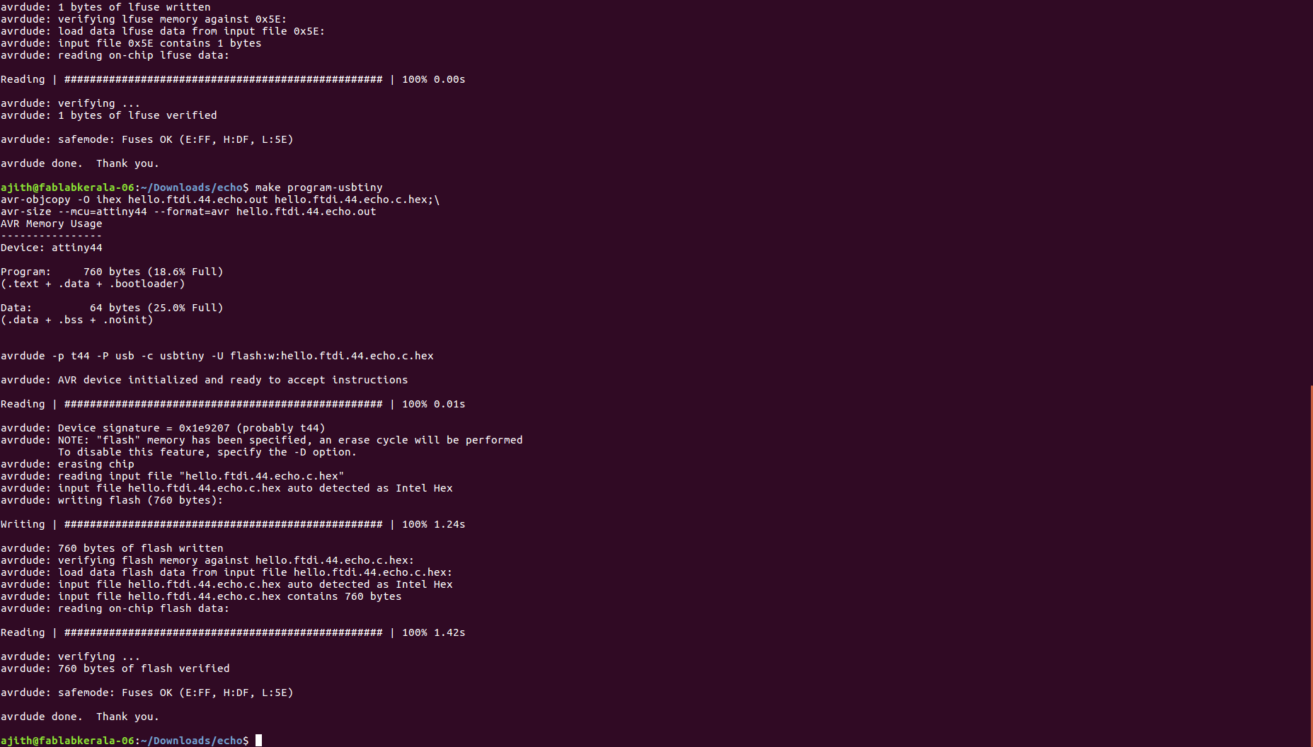
Now the board is successfully programmed and now i can start communicate through the serial communication, FTDI cable can be used for this, first checked the FTDI cable data sheet of FTDI cable as shown below connect the cable to my board in one end and the other end is connected to the computer USB port.
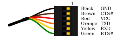
To do the serial communication we need a graphical serial port communications program, I used "Cutecom", installation is simple type sudo apt-get install cutecom from
the terminal. Once installed, we can open the cutecom by typing the command sudo cutecom check the baud rate setting and device Id etc in the console. You can see the settings in the
screenshot given , then click open the device and just input the text one by one in the inupt space , so that it will send to our board and read back to output console of cutecom. Thus i verified that
my echo hellow world board is working perfect.
Download my echo hellow world files (.zip)
Proteus
Strated working with Proteus, installed in windows PC and gone thorugh the tutorial and designed a small circuit. This circuit is a mosquito repeller circuit. Electronic mosquito repellents are equally efficient and relatively safer. The concepts of these mosquito repellers are simple can be done using 555 timer IC and few other commonly available components. I saw this project in circuit digest, the circuit is designed to produce 15kHz frequency and output through a buzzer. I used the demo version of proteus so it doesn't allow to save the files and process. but one thing i loved is, in the same schematic window we can do the simulations.

KiCad
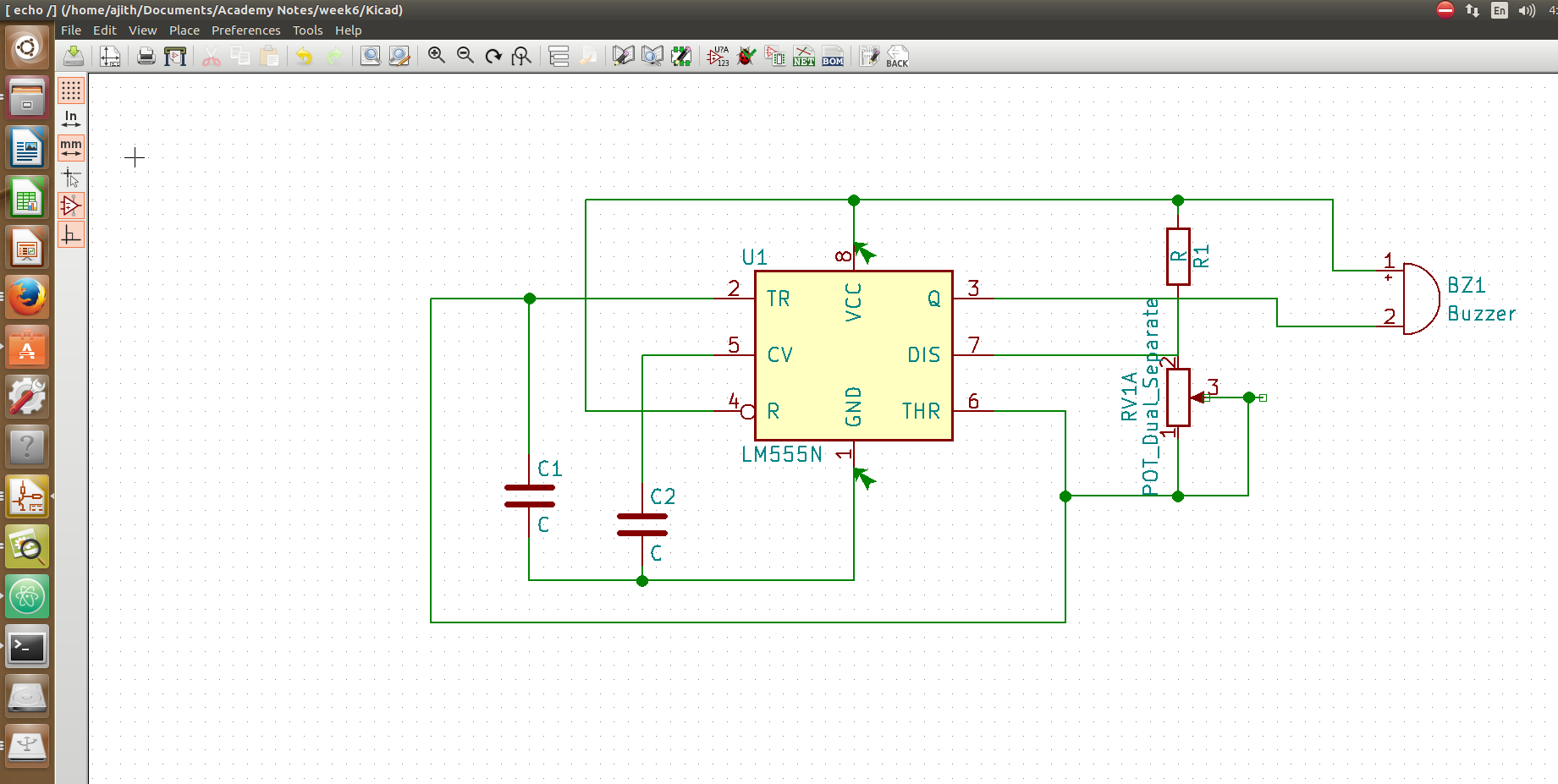
KiCad is an open-source software tool for the creation of electronic schematic diagrams and PCB artwork. I installed the Kicad software from the documentation. The KiCad work-flow is comprised of two main tasks: making the schematic and laying out the board. Both a component library and a footprint library are necessary for these two tasks. KiCad has plenty of both. Just in case that is not enough, KiCad also has the tools necessary to make new ones. I started the design of mosquito repeller in KiCad, as it requires IC555 timer it was there in its default library and placed other components like resistors and capacitors as shown below.

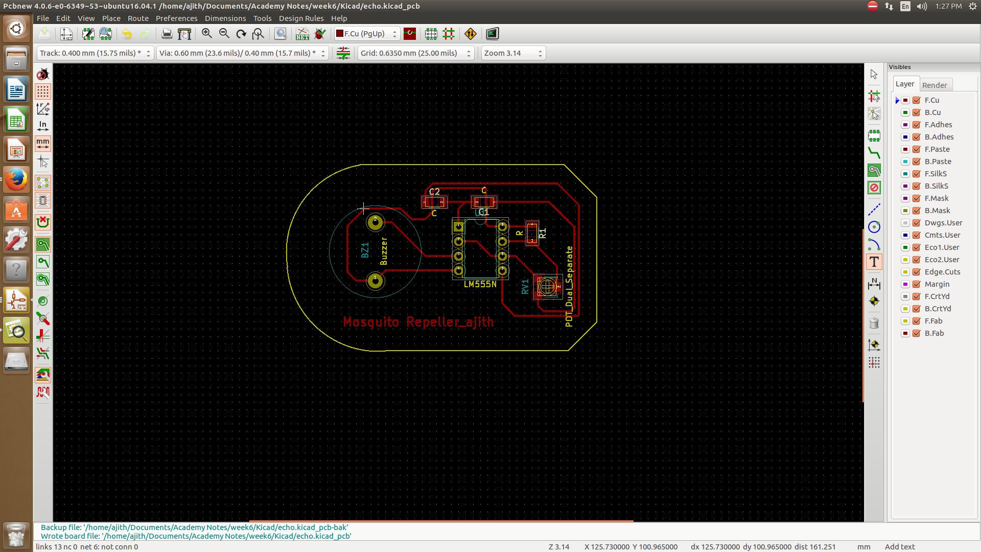
After completing my design i completed the routing of my pcb in the board editor, followed some youtube tutorials and finally i made the pcb as shown below.
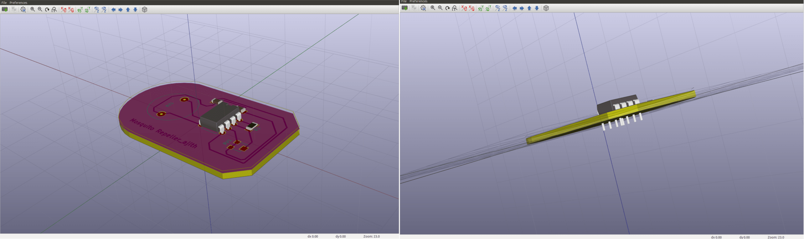
One of the main intersting thing in this software is that we can vie the boards in 3D, i used the 3D viewer option available in Kicad, The below showed image is the 3D view of my mosquito repeller board.
Download My Mosquito repeller files (.zip)
Circuit Simulation
Electronic circuit simulation uses mathematical models to replicate the behavior of an actual electronic device or circuit. Simulation software allows for modeling of circuit operation and is an invaluable analysis tool. It is having the following advantages
| 1. It is much faster to build the circuit in the simulator than in real life |
| 2. If it does not work at first, no harm done. It is easy to adjust and improve. |
| 3. You can access any node in the circuit with a click of the mouse, which makes debugging much faster. |
| 4.You can try components that you do not physically have. |
There are various softwares are available for Analog,Digital,Mixed signal circuits. I have tried two of them and will explain the how the simulations are working.
TINA
Toolkit for Interactive Network Analysis known as TINA Design Suite is a powerful yet affordable circuit simulator and PCB design software package for analyzing, designing, and real time testing of analog, digital, HDL, MCU, and mixed electronic circuits and their PCB layouts. TINA is a paid software and needs a paid license to work with the full features of it. This is basically for windows based systems. I have downloaded the TINA demo version from the TINA demo. It is very easy to simulate tool you can go to the online tutorials for using it, i have used it for simulation of general purpose circuits mainy analog and digital. Using TINA i tried to simulate a low pass filter circuit.
Low Pass Filter
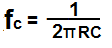
Basically , electronic filter circuits are designed to modify,reshape or reject any unwanted frequencies of an electrical signal and accept or pass only the required signals. A low-pass filter is a filter that passes signals with a frequency lower than a certain cutoff frequency and attenuates signals with frequencies higher than the cutoff frequency. Since capacitive reactance decreases with frequency, the RC circuit shown discriminates against high frequencies. The circuit is an AC voltage divider with an output which falls off at high frequencies at the rate of 6 dB per octave. The cut off frequency of the filter is fc can be calculated by the equation shown below.
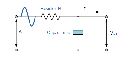
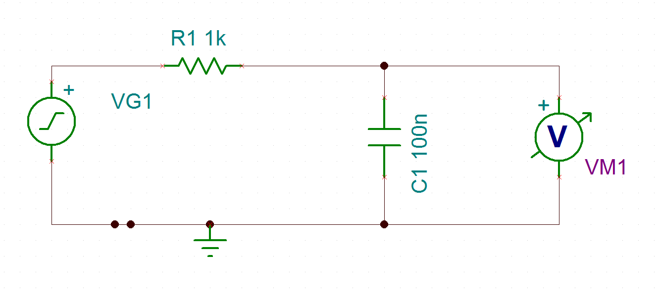
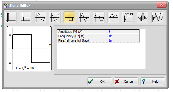
Here using Tina i designed the LPF circuit using a resistor and capacitor, here i have used resistor value as 1K ohm and capacitor value as 0.1uF, So the cut off frequency will come around 1.6KHz. After installation opened Tina and drwan the circuit and in the output connected the voltmeter. If we double click the blocks detailed window will come and we can set the parameters here i selected squqre wave and set the volatge of 5V frequency as 1KHz etc, after that from the transient analysis window we can set the transient analysys option and set the time durations.
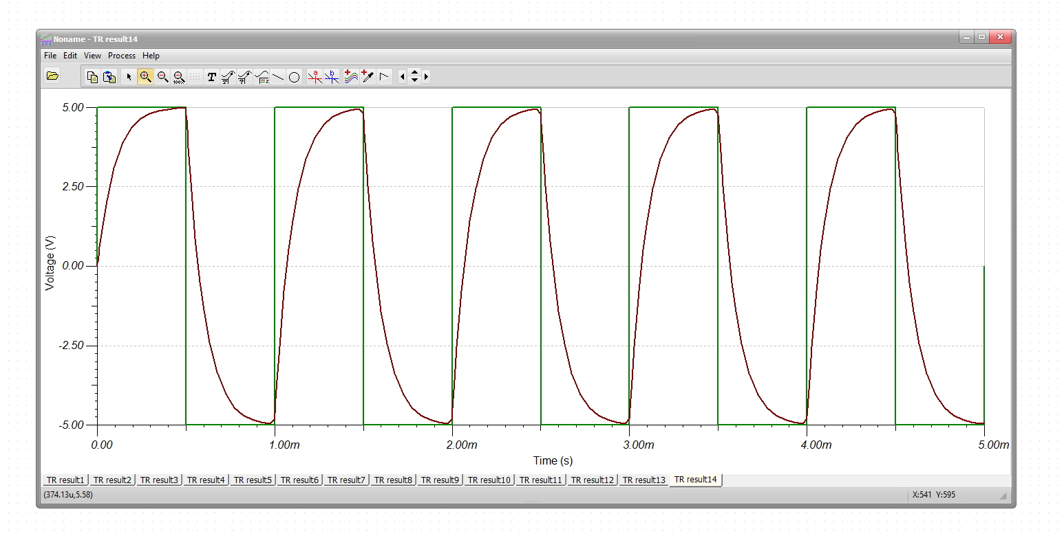
The image shown below shows the parameters i have given for 1KHz frequency, and the transient output i got like the one showed below.
How to verify the Simulation?
Inoreder to verify the simulation of the circuit , I made a test circuit in bread board connected a leaded 1K ohm resistor and 0.1uF capacitor like the LPF configuration then the input to the resistor is connected to the function generator and out put to digital storage oscilloscope. From the signal generator i have set the square wave with the same setting what i have used for the simulation. Using DSO i monitored the input squre wave and the output.
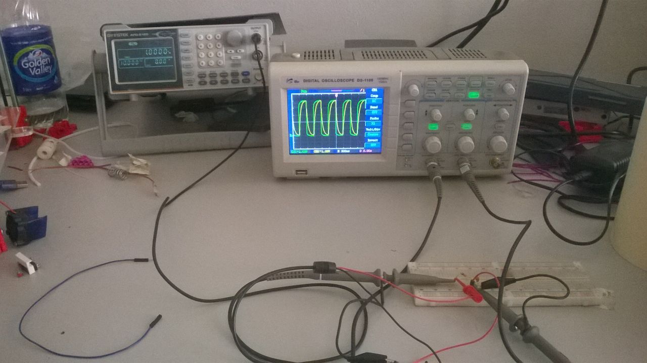
The screenshot below shows the close view of the output. In the figure the green colored line is the square wave input it is little bit noisy while connecting to
bread board using jumper wire the yellow one is the output across the capacitor.
You can compare the out put with the simulation out put on the right side image. It is looking similar, like this we can simulate any circuits.
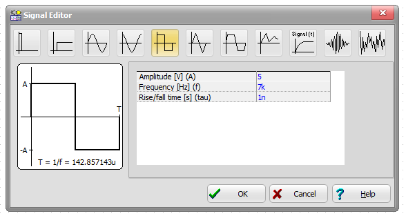
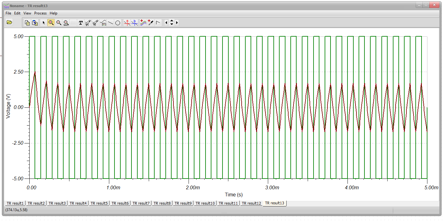
Also taken the transient analysys of the LPF with 7KHz this is beyond the cut of frequency,(the cut off frequency is 1.6KHz) , So the expected out put will be
having lesser gain. You can see the out put of this in the image showed below. Partsim PartSim is a free and full-featured SPICE circuit simulator that runs directly in our browser
PartSim uses a cloud-based version of ngspice, which is an open source simulator based on Berkely's Spice3f5 Spice engine.PartSim schematic editor runs as a
native application in your browser using javascript and doesn't require the use of any plugins. All you need to do is draw your schematic using components that
are available in the tool's sidebar, place your desired current and/or voltage probes,
and then click the "Run" button. This will bring up a simulation dialog box that allows you to run various simulation types (DC, AC, Transient). One of the feature i noted in using this is that
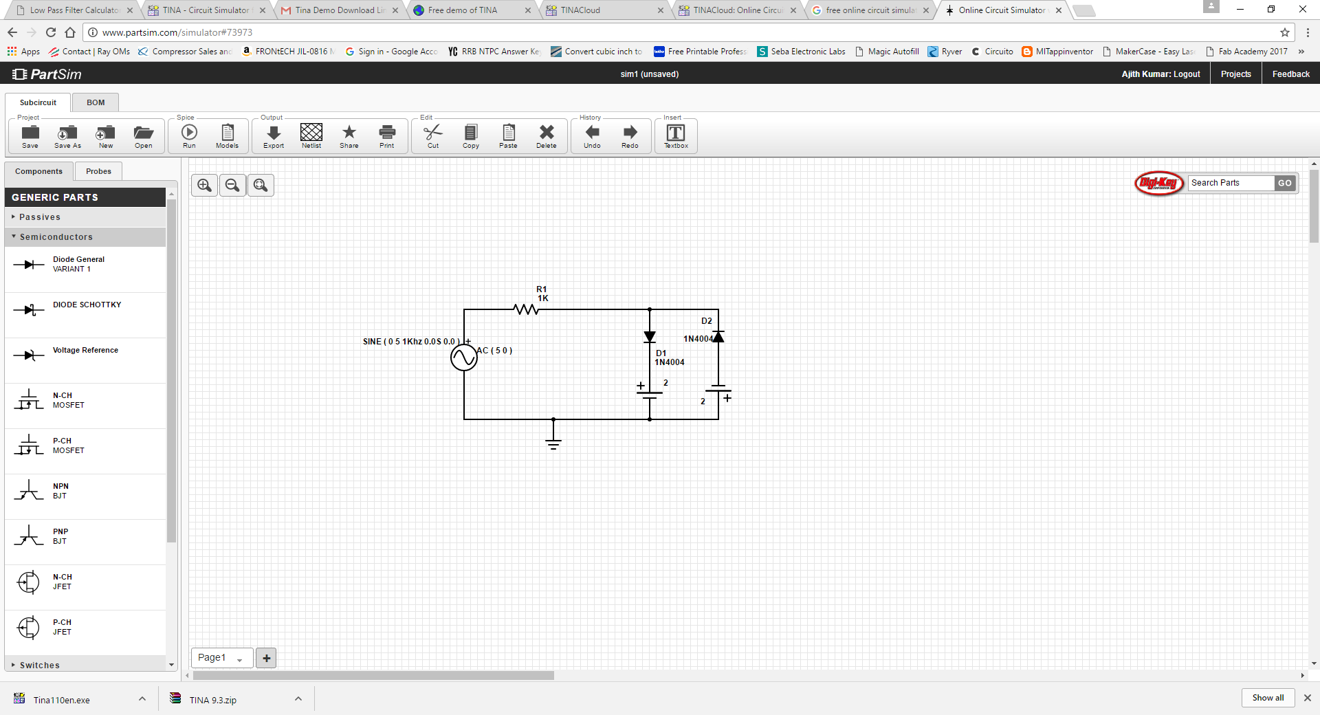
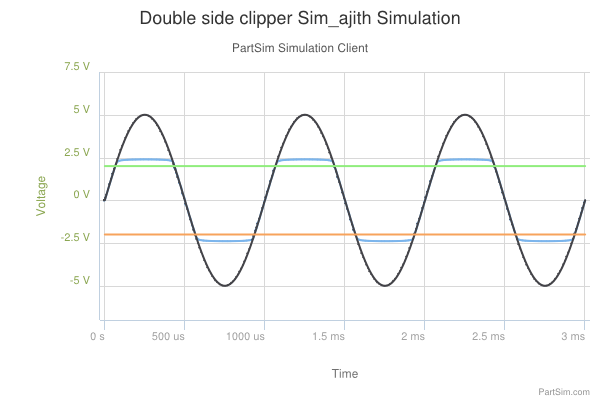
the "Digikey" parts can directly imported through "Digikey par search tool". using this i have simulated a double side diode clipper circuit
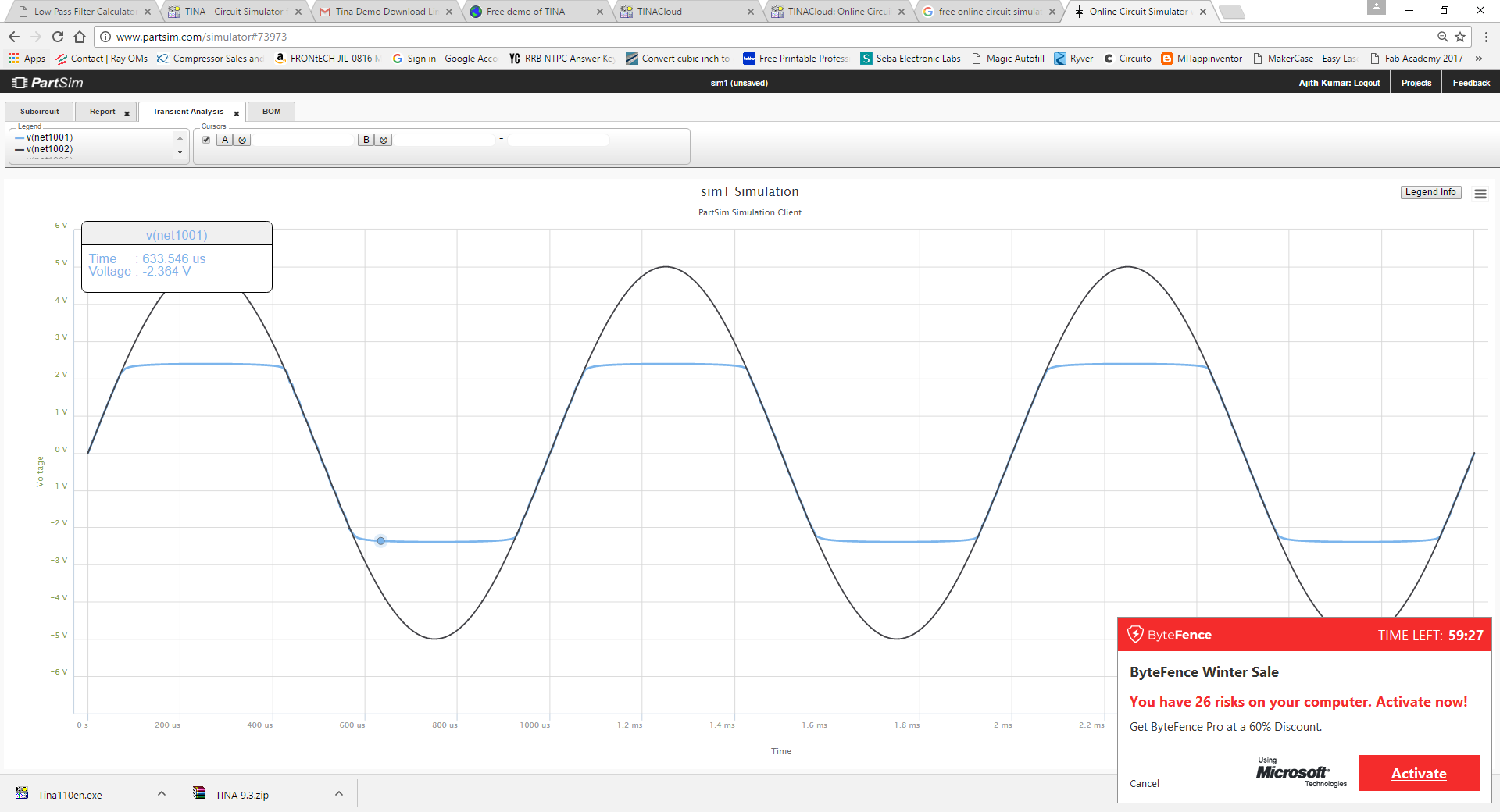
you can check the working of the clipper in the above link. I made the circuit and simulated the result, we can export the output in the form of images(.png),SVG etc. The output exported from partsim in .png form is showed below. You can see the AC sine wave input (Black color), clipped out put (Blue color) and the two biase
voltage levels of +2.5V & -2.5V. We can embed the simulation circuit from partsim like this. Since this is web based we cannot export the schematic file but can share,edit,embed and can export the output. In this week i have familiarised different pcb designing softwares like Eagle, Proteus and KiCAD out of which i loved eagle and KiCAD. Eagle is easy to use and there are better
resources available in internet, But need of paid license to get its full functionalities. Where as KiCAD is free and open source, It is giving all the features , but lack of resources and some times
faced some user inetrface issues. Personally i am happy with Eagle and KiCAD. In the case of circuit simulation softwares i loved proteus beacuse of its features, but one thing irritating me is that even in the trial versions it won't allow to do the things. "You must be the change you wish to see in the world"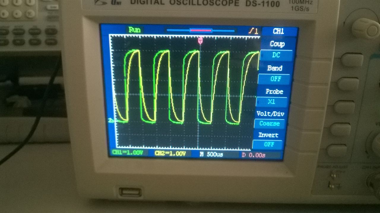
Summary
Quote of the Week