WEEK 4
ELECTRONICS PRODUCTION
ASSIGNMENT
- Make an in-circuit programmer by milling the PCB
Preperation
This week Assignment is to learn about PCB fabrication and mill the Fab ISP board in Modela CNC Machine. I am familier with electronic printed circuit boards and other electronic componenets. Also i have used the modela machine before for making small pcb's and helped somany peoples for making the pcb with modela. I just refreshed about modela operation and pcb designs after Prof.Neil's Lecture.
FAB ISP
FabISP is an in-system programmer for AVR microcontrollers, designed for production within a Fab Lab. There are different versions of ISP's available in the archieve. I selected Brians Version of Fab ISP called "FabTinyISP" for making this week. I already have Neil's Version ISP with me which i made last year for fab use. I sincerely acknowldege the people who worked behind this project for realising FabTiny ISP.
To Know more aboutFabTinyISP
FabTinyISp
It is a ATtiny45 based board having high-performance, low-power Atmel 8-bit AVR RISC-based microcontroller combines 4KB ISP flash memory, 256-Byte EEPROM, 256B SRAM, 6 general purpose I/O lines, 32 general purpose working registers, one 8-bit timer/counter with compare modes, one 8-bit high speed timer/counter, USI, internal and external Interrupts, 4-channel 10-bit A/D converter, programmable watchdog timer with internal oscillator, three software selectable power saving modes, and debugWIRE for on-chip debugging. The device achieves a throughput of 20 MIPS at 20 MHz and operates between 2.7 - 5.5 volts. The main reason to choose this board is that it doesn't have any clock circuits and additional LED's are there to indicating the status of the board while programming. Where, others doesn't have these features before starting the milling the board lets start with the terms dealing with PCB designs for milling.
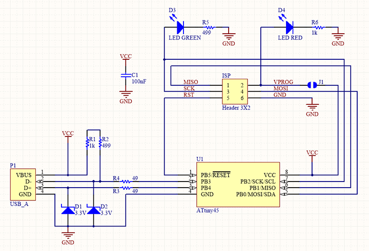
Schematic
A schematic, or schematic diagram, is a representation of the elements of a system using abstract, graphic symbols rather than realistic pictures. A schematic diagram is often used to describe the design of equipment. Here is the schematic of my Fab ISP Board.
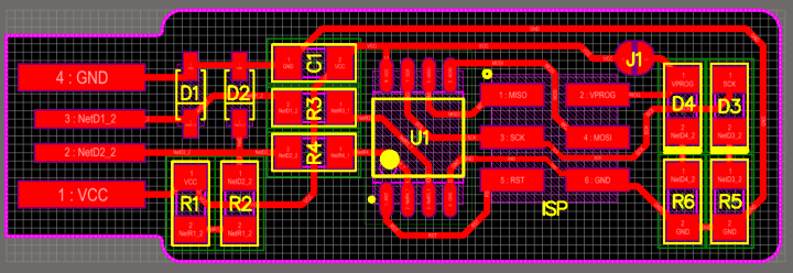
Position Diagram
The position diagram shows the componenet placement in the printed circuit board. Different components will be identified by labels such as for resistors R1,R2 and for capacitors C1,C2 etc. Some components will have polarities, for that the polarity marking will be there (e.g: Diodes, IC's, MOSFET's etc). Using the Board diagram we can place the components for soldering. Here is the ISP Position Diagram.
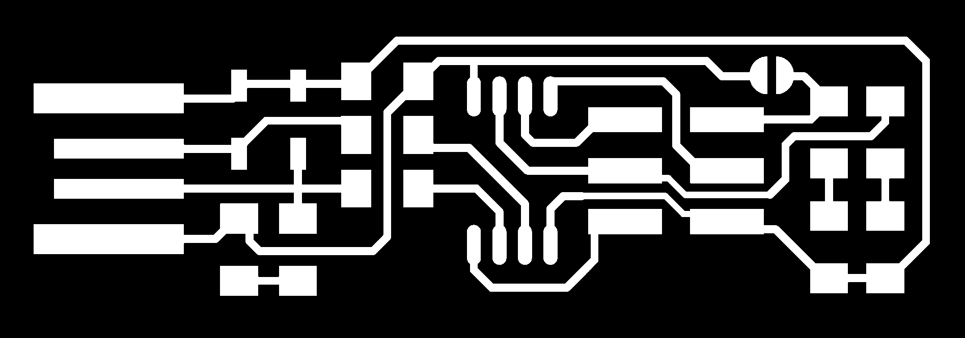
Layout
These are the traces which we are going to transfer to the PCB. The layout is prepared with the help of Electronic CAD softwares like Eagle CAD or Ki CAD. Here is my Layout diagram for ISP. In this one is for Milling the traces in bare copper sheet and other one is for cutting the board.
Milling Traces and cut layout

I have downloaded these layouts from the FabTinyISP documentation page. Now i have to mill my PCB using Modela CNC Machine.
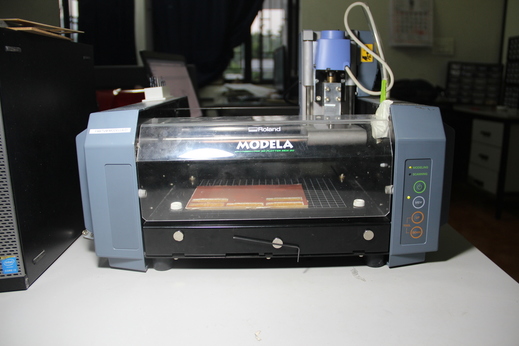
Modela MDX20 Machine
In our Fab lab Modela MDX20 is installed for milling the PCB boards and making molds. Modela MDX20 is a Desktop 3D scanning and Milling machine by Roland. Easy to use,Compatiable with popular softwares, Powerfull and can directly connect to our compuetr via RS232C cable.
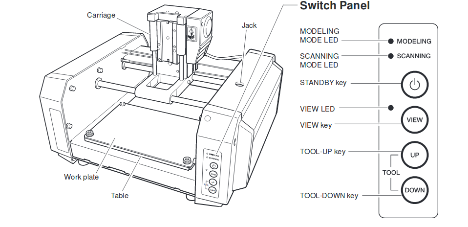
Modela MDX20 Machine
| Work area | 203.2 x 152.4 mm |
| Z stroke | 60.5 mm |
| Spindle speed | 6500 rpm |
Here is the detailed sketch of Modela
Our Instructors Yadu and Vishnu Introduced the Modela machine and its operation to everyone. I am familier with the operation of modela, helped students,startup companies and corporates for doing their projects and development boards. This Video helped me to familiarise the operation of Modela.
Setting the Machine
Step 1
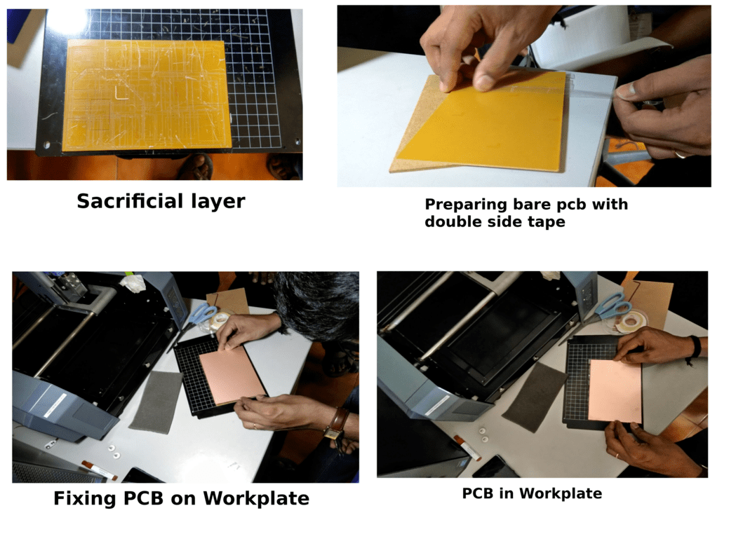
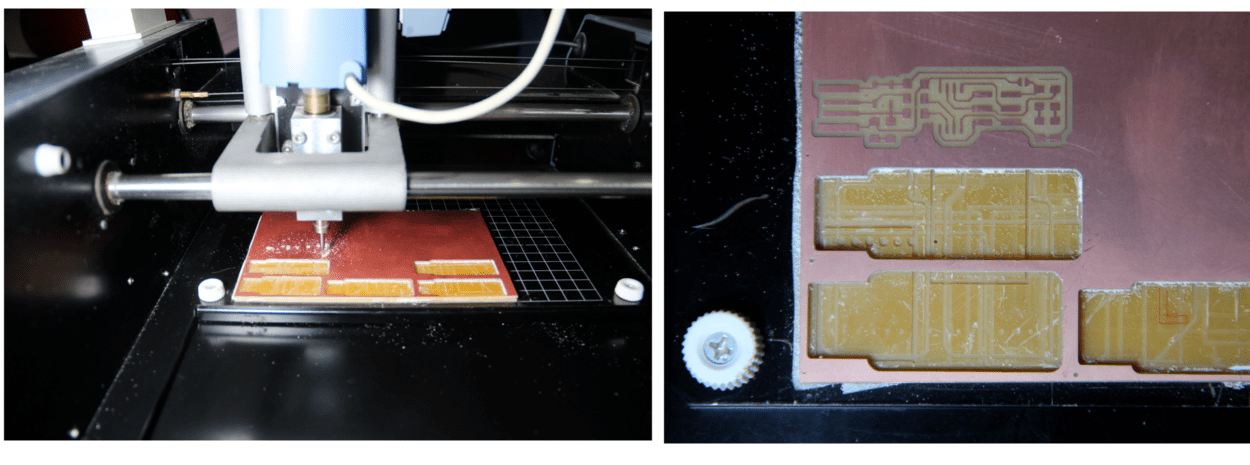
First we have to set the work plate. The work plate is mounted to the table using two screws. Here work plate is acting as "Y". The work plate can be moved outword by pressing the view mode in the front panel of the modela. Unscrew and take out the workplate, this is a metal plate and over this plate we have to fix our bare copper sheet using transparent double side tape. It is better to provide a sacrificial layer inbetween the plate and bare copper board because this will ensure more safety to the machine and bits. Here we used a large single side pcb for total 9 peoples because we can use this single board to mill all the boards. Some of them are already completed their boards, Here you can clearly see the sacrificial layer through the cutout parts.
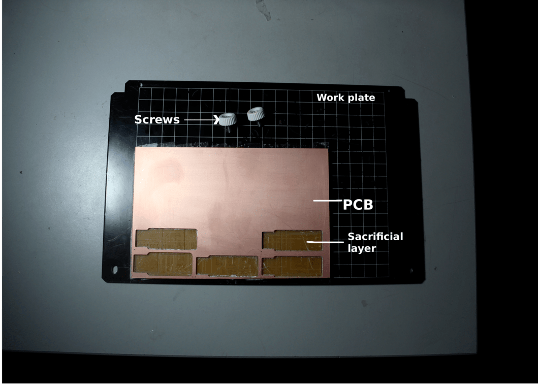
Different steps for fixing the pcb over the work plate is showed below starting from sacrificial layer to the final board.
Step 2
Identifying the Bits
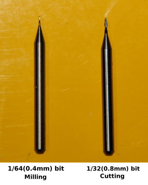
There are different kinds of bits used for milling,cutting pcb boards and for milling the waxes. In modela we have the bits with dia starting from 0.254(0.01inch) to 3.175mm(1/8"). This week inorder to make the pcb we require 1/64 inch(0.396875mm) bit for milling the traces and 1/32inch(0.79375mm)bit for cutting the pcb. We have procured these local bits from India,it is good and cheaper in cost. The dimension of the bits used are same, i.e for milling 0.4mm and 0.8mm for cut out of the board.The bits used are shown below.
Step 3
Machine setup
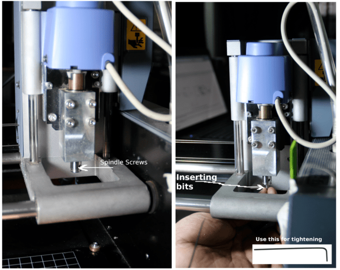
Next we have to setup the machine for milling and cutting. First we have to mill the traces for that turn ON the machine and insert 1/64(0.4mm)bit to the spindle
of the machine using hexagonal wrench(1.5mm). There are two screws facing opposite, tighten the two screws and ensure that the bits are properly placed and there is enough space available in between bottom surface of the carriage and
workplate surface. If you can keep some forms or soft materials just below will save the bit breaking while loading. Want to know more refer this
Step 4
Working with FAB Modules
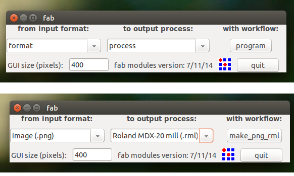
Once the bits are inserted. Open FAB modules through termianl by typing
fab
It will open FAB modules. Fab modules we used are the compiled version of fab modules , we are having some issues with the web modules connecticity with modela machine and tried fab modules html version sometimes it is showing irratic behaviour and bits are getting broken, So i continued with operating with fab modules and decidedto try fab module html locally installed version in the comming weeks with the help of our instructors.
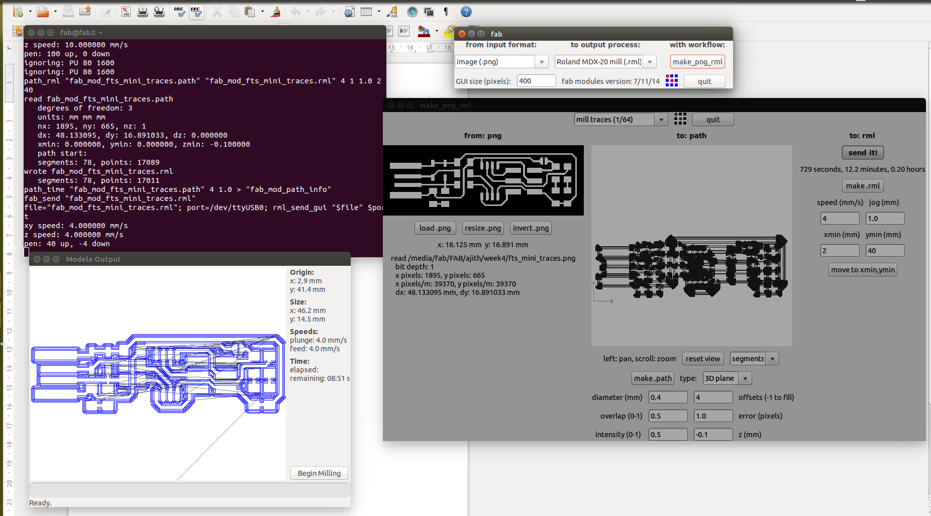
Once opened select the mill trace files and select the bits as "mill traces 1/64". Loaded my image files,Slect the X and Y directions i selected X as 2mm and Y as 40. This will move
the spindle to the corresponding XY position. Once it reached the position, Next we have to set the Z axis for this is done by first loosen the bits by loosening the screws then the bit will touch the top surface of work piece(PCB).
Tighten the bit again carefully on both sides and press the down button very slowly till small copper burr comes out from the pcb, this will ensure proper zeroing the Z axis. Also ensure the space between the head carriege and the metal end otherwise the bit
cannot move further downwards. Next we have to set the offsets and errors on the fabmodules. Offset is the number of paths it make in between two tarcks, i have given it as 4, So it will go four paths and error pixels i have given the value 1.
AYopu can refer the settings i have given as in the picture below. Press make .path ,then make.rml and click send it. New window will open contains the paths here if we press begin milling will
start the milling.
Here is the picture showing modela started milling the pcb on the copper sheet.
Step 5
Cutting the board
After completing the milling next is cutting the board for that open the fab modules like we did in the previous step and this time we have to open out cut traces file. Select the 1/32(0.8mm) bit for cutting and leave the settings as such. Set X and Y axis as before for my case it is X-2mm,Y-40mm Z axis can be set like the previous steps.
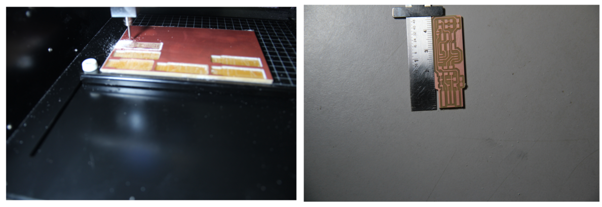
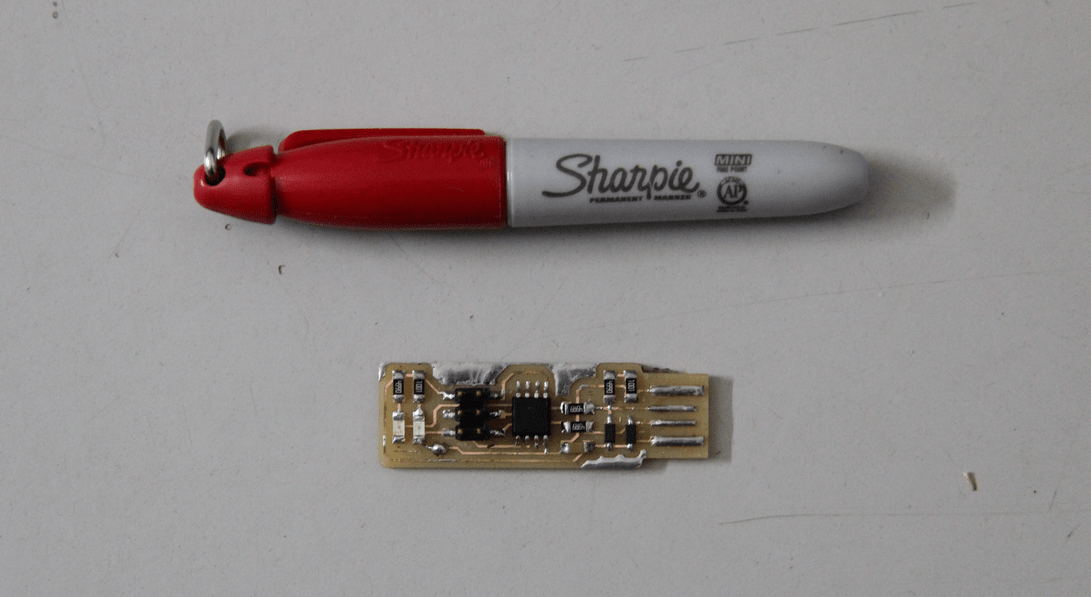
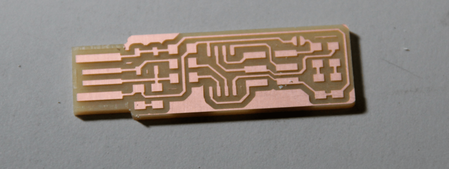
I removed the extra copper available in the USB connector area by using a Knief. My FAB ISP board is ready for soldering now
Soldering the Board
Soldering is to fix the componets over the PCB using soldering iron and lead wire. Here weller WSE51 soldering station is available in our lab. Before soldering we have to prepare the bill of materials(BOM). i have prepared a BOM for my FAB ISP.
| ATtiny45 | 1 No |
| Resistor 1KΩ | 2 Nos |
| Resistor 499Ω | 2 Nos |
| Resistor 49Ω | 2 Nos |
| Zener 3.3V | 2 Nos |
| LED Red | 1 No |
| LED Green | 1 No |
| Capacitor 100nF | 1 No | IDC connector 2X3 | 1 No |
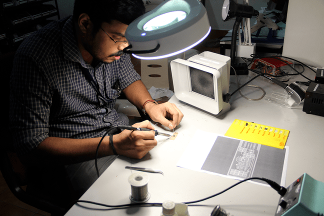
After collecting components from inventory, started soldering of my board using the soldering iron. I know about soldering SMD componenets both reflow and manual soldering, currently we don't have any solder paste to try out reflow soldering so started soldering with soldering station. If you wanted to know more about soldering check this Video
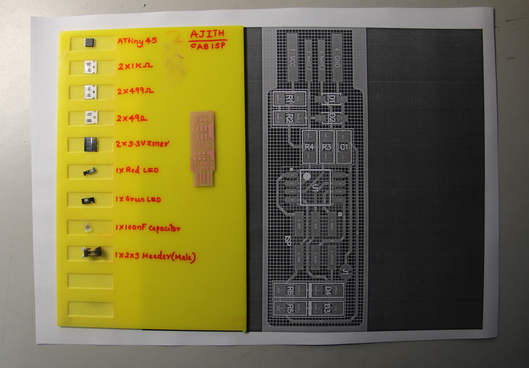
All components collected from the inventory is arranged in a plate, which the students made last year using yellow acrylic and is having slots for keeping SMD componenets. After collecting all the components for my pcb started soldering, the polarities of diodes and IC were checked parallely with schematics print.Final hereo shot of my pcb after soldering is showed below.
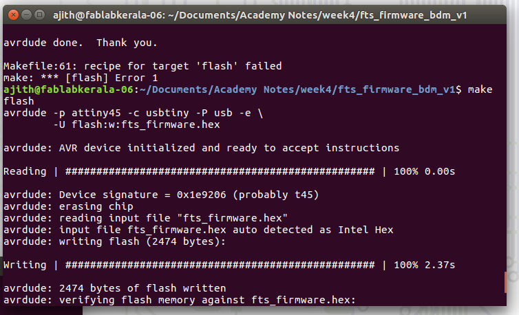
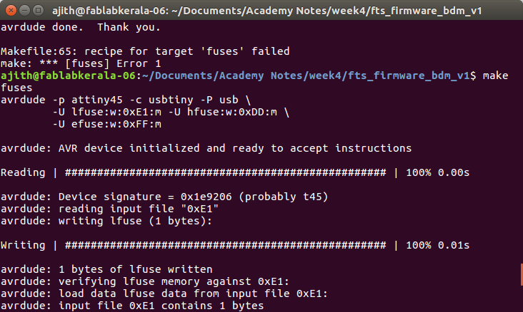
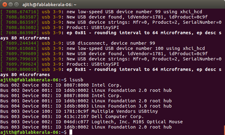
Programming FAB ISP
I followed Brians documentation for thiis part. Installed avr dude ,downloaded source code files and followed the steps to program it. Here i have taken my old Neil's version ISP as programmer. Every thing worked fine except some communication issues with my old ISP, when i adjusted the cable it got cleared. I completed all the steps except the final step.
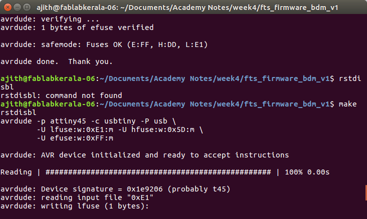
These are the snaps of my isp programming
First two picture shows the make flash and make fuse command running stages, third one shows my board detection using lsusb command in terminal you can see my ISP is got detected as "Multiple vendors USBtiny" and the final one shows the rstdisbl command.
Changes I made
As per Brians documentation finally we have to remove the solder bridge to disconnect VCC from the Vprog pin on the ISP header. When i removed and tried to program other ISP boards it is not working. Our insrtuctor Vishnu told the problem is due to the removal of solder bridge. After going through the documentation, I found that by removing the solder bridge the power to the ISP header is opened due to this we can't program other boards because the boards won't get any power. In that case we have to provide external power to the boards. Here i leaved the solderbridge as it is, then i noticed that now my ISP is able to program other boards.
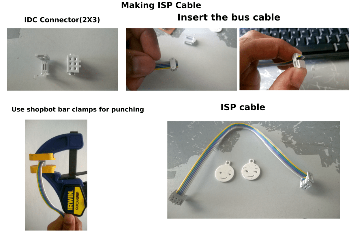
After programming my board i made a cable for my ISP using this cable i can programm other boards. The steps i followed is shown below it requires only two numbers of 2X3 ISP female header connectors and 20cm long data cable of 6 bus wires
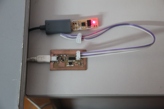
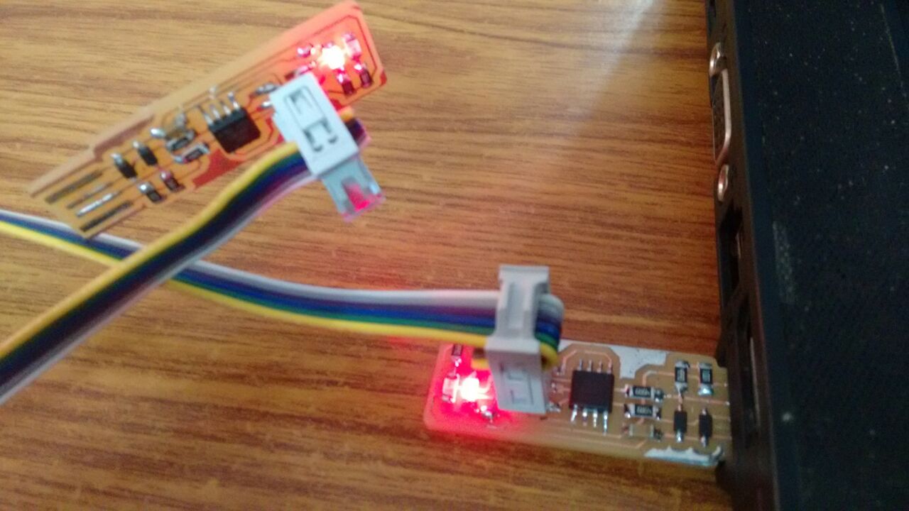
Next i used my programmer to program Jim's Fab ISP it worked fine. The ISP connected to the USB port is mine , It is better to connect the ISP using a USB extender.
Here is the Hero shot of my Fab ISP board