FINAL PROJECT
EASY TESTER
FINAL PROJECT DRAFT
In Fab Academy last two weeks we have to make a product using the machineries and skills we learned from Fab Academy. Actually I am from Electronics background and interested in doing embedded projects , Many ideas came into my mind for final project but, I thought of making something use full for Fab Lab . I have seen that many of the projects are being not used after the academy So, I decided to make something that can be usefull for the daily activities. I have seen most of the academy projects are based on machine making kind of projects. I planned to make an Insrtument which can test and measure SMD and leaded componenets. In fab Lab there are hand held multimeters and are used for measuring the SMD components, but it is having some limitations that SMD capacitors and other active devices can't tested. If we are using such multimeter it need a special care while handling SMD devices sometimes it may explod from the probs. Noraml multimeters is having two probe wires having long lenght cable wires, so it will be difficult for a single person to probe it and take the reading. In such cases we are using Smart tweezers, these are the insrtruments like multimeter but specially made for the measurement of SMD componenets. Still some limitation are there, in smart tweezers measuring three terminal active devices like transistors and mosfets are not posiible.
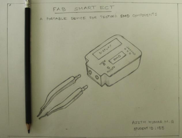
I am planning a portable device with SMD measuring capability, easily detachable tweezer probes for testing on board components and leaded componenets. Selected Atmega328 as its core and other sensing and measuring circuits for the measurement purposes ,finally it will be displayed on LCD / other displays. I have alreday done initial testings using Arduino Uno board for measuring Resistance and capacitance and is working successfully. Here is the proposed sketch for it.
PROJECT DEVELOPMENT
CASE STUDY
When the idea came into my mind i have done a study on it. I had used smart tweezers for measuring SMD devices and is very easy in measuring SMD, i have been here for more than one year and what i observed is many of the students are getting trouble while dealing with SMD devices, if they are not from an engineering background the chances of difficulty is more. Also there are no provision to check transistors , MOSFETS and other devices. What they do is if any failure comes means they simply replace the componenet without any analysis. If we lookinto that also will be difficult why because for testing such kind of devices with normal multimeter is little time consuming and needs a lot of technical knowledge. If it is in the case of passive devices then using normal hand held multimeter requires a help from others.
PROOF OF CONCEPT
I have gone through several schematic circuits on sensing resitors , capacitors and other active devices. I have tried some circuits in arduino uno board availablke in our lab mainly resistance and capacitance measurements. In my input devices week i have tried a resistance measurement and displayed it to the LCD display using attiny44.
Initially i gave FAB SMART METER as the name for my project but later i changed it to Easy Tester, as it is easy to test the componenets.
EASY TESTER
Easy Tester is an electronic componenet tester made in fab lab with major componenets from fab inventory and needs few passive and active componenets. It is intended to meet the componenet testing of fab inventory. In fab inventory all are SMD componenets, but in our local market the availability of SMD componenets is less compared to leaded. I cannot avoid both types because we are using both types, then planned to make an instrument which can be use for both SMD and leaded and made the design accordingly.
Features
The main features of Easy Tester are shown below
- Resistance , capacitance, Inductance of SMD and Leaded components.
- Testing of Active components like Diode,Transistor,MOSFET, LED etc.
- PWM and Frequency measurements
- Auto power OFF options
- Portable probes for measuring SMD on board componenets
- External programming and communication interfaces
- Automatic pinout detection
- Zener Voltage detection with extra circuits
- Special protection circuits for Atmega input pins
I. Electronic Design
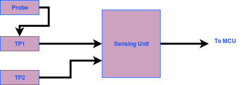
Block diagram
Block diagram of Easy tester is shown below.
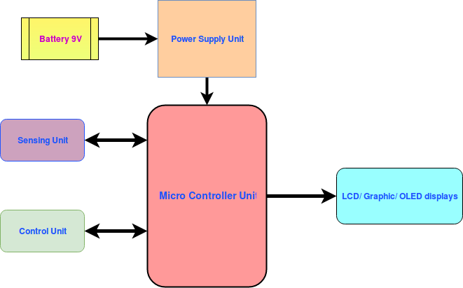
The total system can be divided into five different units.
- Power Supply Unit
- Microcontroller Unit
- Sensing Unit
- Display Unit
- Control Unit
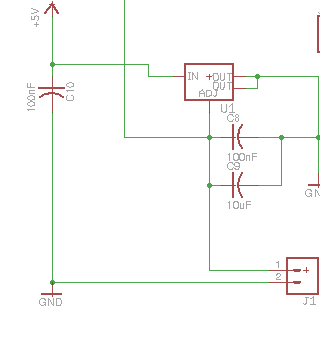
Power Supply Unit
Power supply unit is providing appropriate supply voltage for the microcontroller and other units for its operation. In my circuit i have given provision for Battery operating mode a 9V battery is used for this purpose. Also there are provisions given for connecting usb connectors for connecting the micro usb data cables there by it will operate without batter. In this i have used LM2940IMP - 5.0 a 5.00V ,1A voltage regulator which is available in our fab inventory. There is some mistake in the pinouts of foot prints in fab library for the regulator in fab library, this i have noticed earlier with the datasheet and i corrected the schematic according to the data sheet. The power supply circuit can be operated in two modes :
(i)Normal Mode
(ii)Power saving mode
(i)Normal Mode
In normal mode the voltage regulator is directly connected to the battery through a switch. The power from 9V battery is converted to 5V using 5.0V,1A regulator in the circuit and the output is fed to all other circuits. J1 connector is used for this purpose which is shown below.
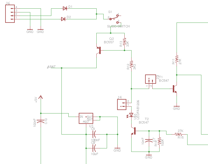
(ii) Power saving mode
I planned a power saving scheme in my circuit, since every time the battery is powering the circuit the battery will easily drain out, inorder to avoid this a powering scheme is adopted. It is having circuits with transistors for switching the voltage regulator and starting the tests. The circuit is implemented but not configured to operate in this mode, i need to change the programm which i am planning as next phase. The circuit for this is shown below.
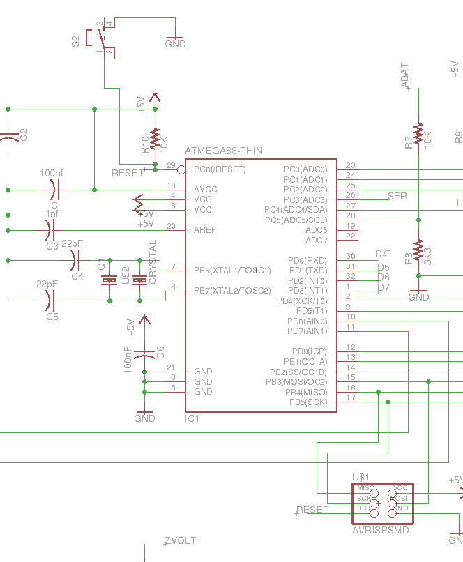
Micro controller unit
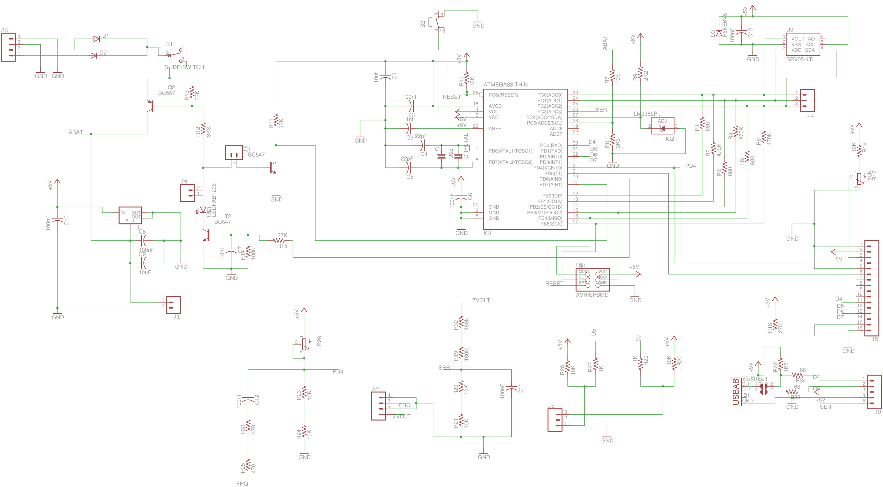
Micro controller unit is the main processing part in the design. Micro controller will sense/measures the data from the input devices and it will process the data , finally displayed to the output unit. Here i have used Atmega328P as the microcontroller, with 8MHz crystal oscillator and other circuits. It is provided with ISP programming ports and reset circuitaries. In my schematics i planned a SMD type crystal oscillator but due to the non availability of the item , paralleley i have provided pads to fixing leaded type crystal. The schematic is shown below.
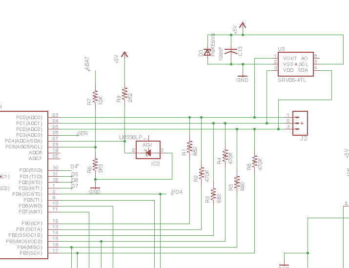
Sensing Unit
Sensing unit senses the input data and transffered to the microcontroller unit. This unit mainly consist of sensor circuitary for the measurement of passive and active componenets. In the micro controller PC0,PC1 & PC2 are identified for sensing and testing the active and passive componenets and is terminated into TP1 connector. TP1 is having three pin connectors and will be placed on the top of the tester. TP2 is another three pin sense connector which is used to measure the frequency, zener voltages and common GND. TP1 is having another parallel connection to the portable probs which is placed on the side wall of the tester, can be used for the measurement of SMD componenets. Atmega input pins are to be protected from large residual volteges during the capacitor measurements and from the ESD (Electro static discharge). I have added the protection circuit using SRV05-04TL ;a surge suppressor diode array to the PC0, PC1 & PC2 pins of the Atmega. The main sensing circuit is shown below.
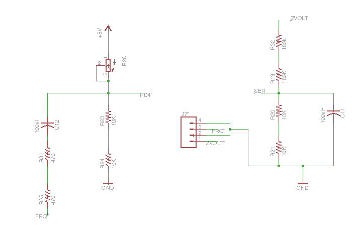
Frequency measuring circuits are seperate circuits which is connected to the PD4 pin of the Atmega and the Zener voltage testing circuit is connected to PC3 of Atmega. PD4 is also connected to LCD display LCD-RS signal, As PD4 can be used as input port as long as no out put to the LCD is required. The circuit of both are shown below.
Control Unit
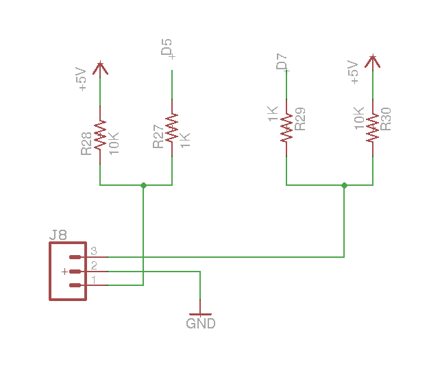
Contol unit comprises for menu controlling circuits and test start circuits. A rortary encoder is planned for the selection of menu functions alternately the menu can be contolled using a push button. Here i used a push button for starting the test and selecting the menu, the MCU will detect the duration of the push button press time and we can programm to select different functions. Connector J3 is used for connecting the start/menu button and connector J8 is for connecting the rotary encoders. The schematic of the rotary encoder is shown below.
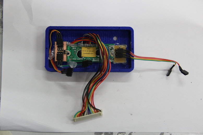
Display Unit
This is the final out put display section, where the measured data is displayed. In my design i planned for connecting with 16X2 LCD display available in fab inventory. The connections are shown in the final schematic. I have done the testing of the LCD in my output devices week and i am confident in that circuit. Also we can connect the graphic or OLED displays so that the system becomes very small, I thought to make it with LCD , as its an available item in any fab labs.
Final schematic
All the above circuits are drawn in eagle software and the full schematic is shown below. After completing the schematic i have checked the netlist manually with the help of Renjith, inorder to confirm what i have drawn is correct.
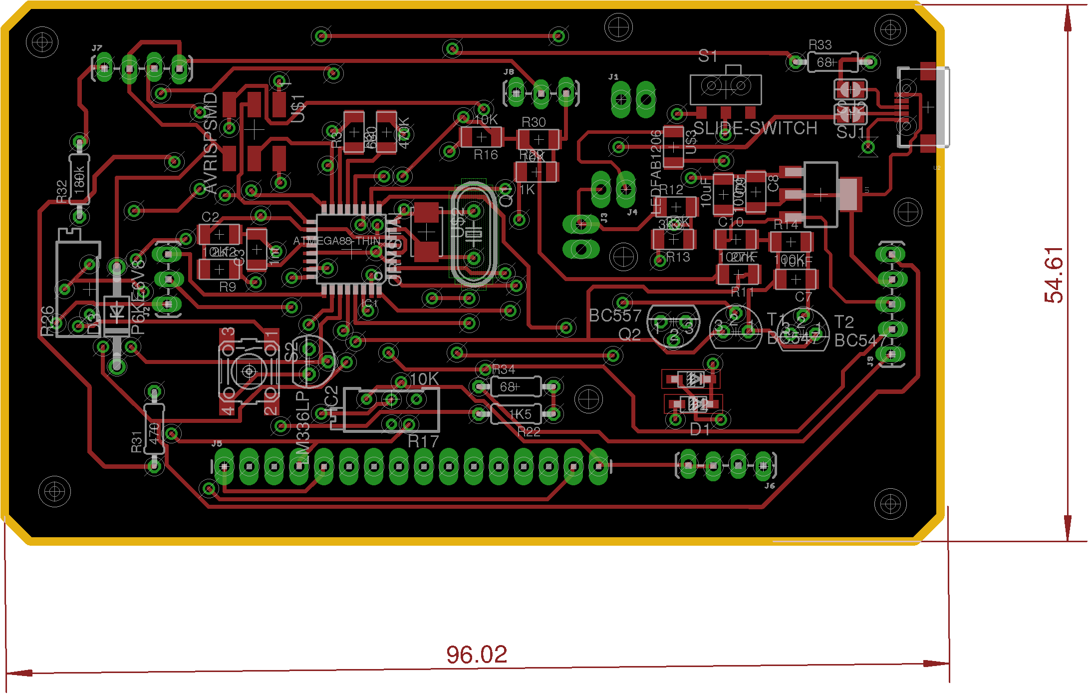
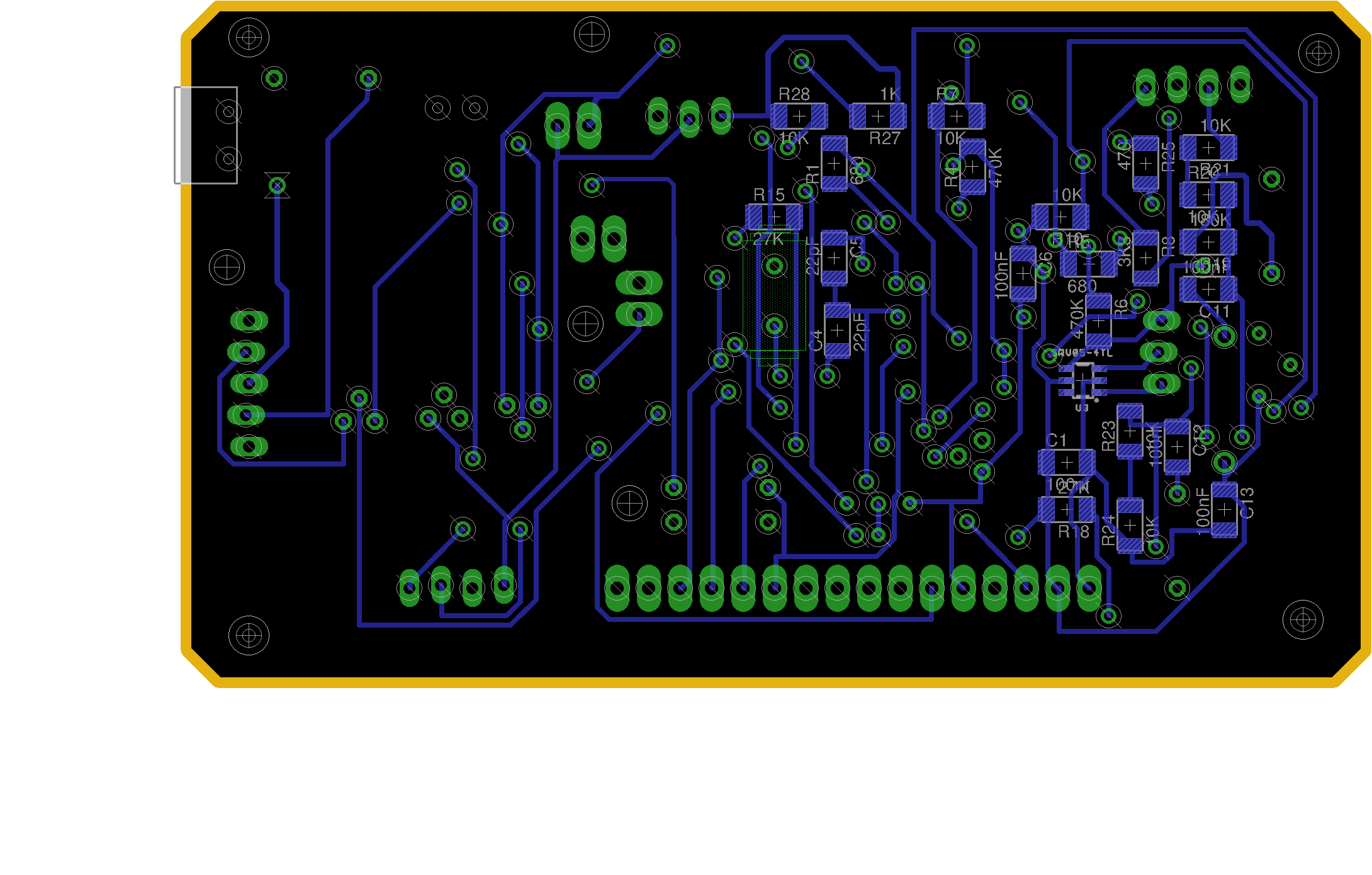
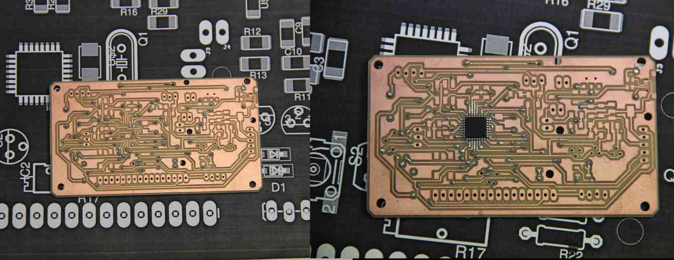
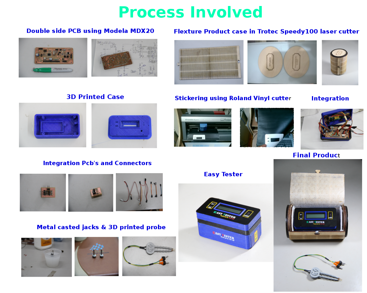
After the netlist verification, i have done the ERC checks and got lot of errors which i corrected later and started the board layout. First arranged all the componenets in proper place and it was showing bigger in size , So i planned to make a double sided pcb. The design rules were setted to process the pcb in modela and then made a plan to position to place the components in top and bottom side. Few componenets were placed in the bottom side and checked with autorouter and got almost 75% routed then i manually routed the remaining connections and finished the layout. In the below showed image is the top and bottom view of my pcb with its dimension. Also checked the DRC checks and the corrections had made.
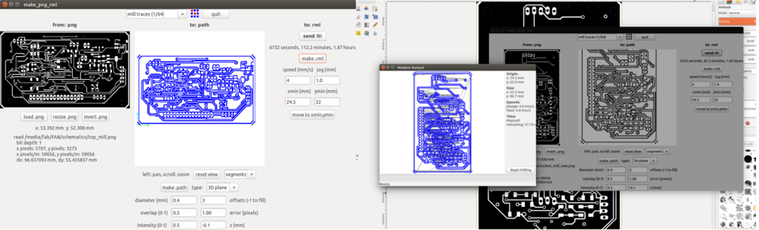
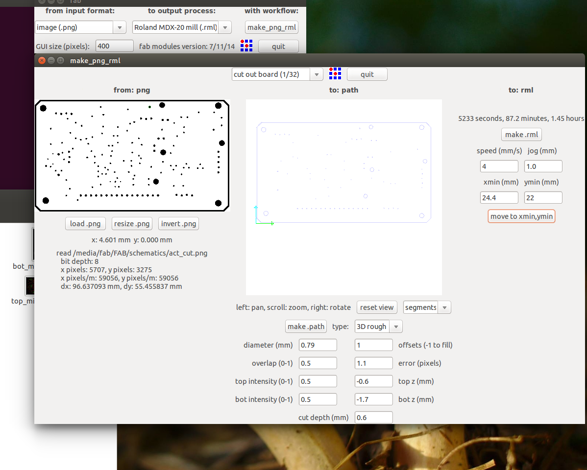
Next step is to prepare the files to process with modela cnc machine. Milling the pcb we require top and bottom png images and for drilling and cutting image file. Exported the file and edited in gimp. The files for the milling and cutting is shown below.
Mill traces Top layer
Mill traces Bottom layer
Cutting and drilling
Before starting the pcb routing i thought to make the Bill of materials and making connector deatails. I have ordered the componenets which are not available in lab locally, my plan was to finish the soldering of first batch componenets and by that time rest of the components will arrive.
Download Easy Tester PCB Fabrication files (.zip)
Bill of materials
| Sl.No | Components | Qty(Nos) | Cost per Item ₹ (INR) | Total Price |
|---|---|---|---|---|
| 1 | Atmega328P-AU | 1 | 110.00 | 110.00 | 2 | LM2940IMP-5.0CT-ND | 1 | 100.00 | 100.00 |
| 3 | LM336LP 2.5V | 1 | 37.00 | 37.00 |
| 4 | Diode schottky 1A 100V | 2 | 12.00 | 24.00 |
| 5 | P6KE6V8- 6.8V Zener Diode | 1 | 20.00 | 20.00 |
| 6 | Capacitor- 100nF, 1206SMD | 7 | 4.00 | 28.00 |
| 7 | Capacitor- 10uF, 1206SMD | 2 | 4.00 | 8.00 |
| 8 | Capacitor- 10nF, 1206SMD | 1 | 4.00 | 4.00 |
| 9 | Capacitor- 1nF, 1206SMD | 1 | 4.00 | 4.00 |
| 10 | Capacitor-22pF, 1206SMD | 2 | 4.00 | 8.00 |
| 11 | Crystal-8MHz SMD/Leaded | 1 | 15.00 | 15.00 |
| 12 | Transistor-BC547 | 2 | 5.00 | 10.00 |
| 13 | Transistor-BC557 | 1 | 5.00 | 5.00 |
| 14 | SRV05-4TL- Surge suppressor | 1 | 47.00 | 47.00 |
| 15 | Resistor- 680 ohm SMD1206 | 3 | 0.25 | 0.75 |
| 16 | Resistor- 470 Kohm SMD1206 | 3 | 0.25 | 0.75 |
| 17 | Resistor- 10 Kohm SMD1206 | 9 | 0.25 | 2.25 |
| 18 | Resistor- 3.3 Kohm SMD1206 | 2 | 0.25 | 0.50 |
| 19 | Resistor- 2.2 Kohm SMD1206 | 1 | 0.25 | 0.25 |
| 20 | Resistor- 27 Kohm SMD1206 | 3 | 0.25 | 0.75 |
| 21 | Resistor- 33 Kohm SMD1206 | 1 | 0.25 | 0.25 |
| 22 | Resistor- 100 Kohm SMD1206 | 1 | 0.25 | 0.25 |
| 23 | Resistor- 180 Kohm SMD1206 | 1 | 0.25 | 0.25 |
| 24 | Resistor- 1.5 Kohm SMD1206 | 1 | 0.25 | 0.25 |
| 25 | Resistor- 470 ohm SMD1206 | 1 | 0.25 | 0.25 |
| 26 | Resistor- 1 Kohm SMD1206 | 2 | 0.25 | 0.50 |
| 27 | Resistor- 68 ohm Leaded | 2 | 0.50 | 1.00 |
| 28 | Potentiometer (variable Resistor)- 10 Kohm | 2 | 10.00 | 20.00 |
| 29 | LED SMD1206 | 1 | 6.00 | 6.00 |
| 30 | Slide Switch SMD | 1 | 15.00 | 15.00 |
| 31 | Push button switch SMD | 1 | 30.00 | 30.00 |
| 32 | ISP Header | 1 | 10.00 | 10.00 |
| 33 | Connector Header 1X02 | 3 | - | - |
| 34 | Connector Header 1X03 | 2 | - | - |
| 35 | Connector Header 1X04 | 2 | - | - |
| 36 | Connector Header 1X05 | 1 | - | - |
| 37 | Connector Header 1X16 | 1 | 20.00 | 20.00 |
| 38 | LED leaded -Red | 1 | 1.50 | 1.50 |
| 39 | Push button switch 6mm | 1 | 10.00 | 10.00 |
| 40 | Connector jack female | 2 | 56.00 | 112.00 |
| 41 | Slide switch 6mm | 1 | 10.00 | 10.00 |
| 42 | 9V Battery snap | 1 | 10.00 | 10.00 |
| 43 | 16x2 LCD Display | 1 | 150.00 | 150.00 |
| 44 | 9V Battery | 1 | 250.00 | 250.00 |
| Total Cost Of componenets in ₹ (INR) | ₹ 1072.50 or 16.50 USD |
Connector mapping
Connector mapping will help us to understand the signals comming in each connectors and it will be helpful for the integration and trouble shooting purposes. I have done mapping of connectors and its individual deatils.
| Connector ID | Description |
|---|---|
| Connector- J1 - 2 pin connector | 9V Supply connector- Normal Mode |
| Connector- J2 - 3 pin connector | Test Pin connector TP1 |
| Connector- J3 - 2 pin connector | Test Start connector |
| Connector- J4 - 2 pin connector | LED Indicator |
| Connector- J5 - 16 pin connector | LCD interface connector |
| Connector- J6 - 4 pin connector | 9V supply connector - Power saving mode |
| Connector- J7 - 4 pin connector | Test Pin connector TP2 |
| Connector- J8 - 3 pin connector | Rotary Encoder connector |
| Connector- J9 - 3 pin connector | Rotary Encoder connector |
Connector Details
| Connector Pin No. | Description | Remarks |
|---|---|---|
| J1-1 | +9V | |
| J1-2 | GND |
| Connector Pin No. | Description | Remarks |
|---|---|---|
| J2-1 | TP1- Test Pin No 1 | |
| J2-2 | TP1- Test Pin No 2 | |
| J2-3 | TP1- Test Pin No 3 |
| Connector Pin No. | Description | Remarks |
|---|---|---|
| J3-1 | Start button High | |
| J3-2 | Start button Low |
| Connector Pin No. | Description | Remarks |
|---|---|---|
| J4-1 | LED Indicator Low(Cathode) | |
| J4-2 | LED Indicator High(Anode) |
| Connector Pin No. | Description | Remarks |
|---|---|---|
| J5-1 | LCD Pin No.1- GND | |
| J5-2 | LCD Pin No.2 - +5V VCC | |
| J5-3 | LCD Pin No.3 - VEE | |
| J5-4 | LCD Pin No.4 - RS | |
| J5-5 | LCD Pin No.5 - R/W (GND) | |
| J5-6 | LCD Pin No.6 - Enable | |
| J5-11 | LCD Pin No.11 - D4 | |
| J5-12 | LCD Pin No.12 - D3 | |
| J5-13 | LCD Pin No.13 - D2 | |
| J5-14 | LCD Pin No.14 - D1 | |
| J5-15 | LCD Pin No.15 - VCC | J5-16 | LCD Pin No.16 - GND |
| Connector Pin No. | Description | Remarks |
|---|---|---|
| J6-1 | +9V supply High | |
| J6-2 | +9V supply High | |
| J6-3 | GND | |
| J6-4 | GND |
| Connector Pin No. | Description | Remarks |
|---|---|---|
| J7-1 | Zener Voltage | |
| J7-2 | GND | |
| J7-3 | FREQ INPUT | |
| J7-4 | GND |
| Connector Pin No. | Description | Remarks |
|---|---|---|
| J8-1 | Rotary encoder -CLK | |
| J8-2 | GND | |
| J8-3 | Rotary encoder -DT |
| Connector Pin No. | Description | Remarks |
|---|---|---|
| J9-1 | Serial communication Rx | |
| J9-2 | Serial communication Tx | |
| J9-3 | +5V VCC | |
| J9-4 | GND | |
| J9-5 | PC3 out |
PCB Fabrication
Next step is Milling of PCB, for that we require milling and cutting files, which i have created using eagle software. I wanted to make a double sided pcb in Modela Mdx20 machine. I made a setup for making the double sided pcb's You can refer my input devices week documentation for doing double sided pcb. First we need to fix the X and Y origins so that it won't change while doing the bottom layer milling.
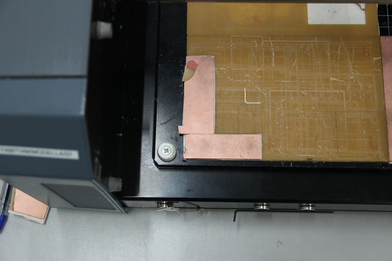
After fixing the X and Y origins i have done some trials to findout the exact coordinates by drilling a 0.8mm hole on the top and bottom of the pcb, for that i have created a small circular dot in gimp and exported into png file. checked the orientation of the holes and done some more trials to match the hole orientations. Finally i found the X and Y origins and then fixed actual pcb.
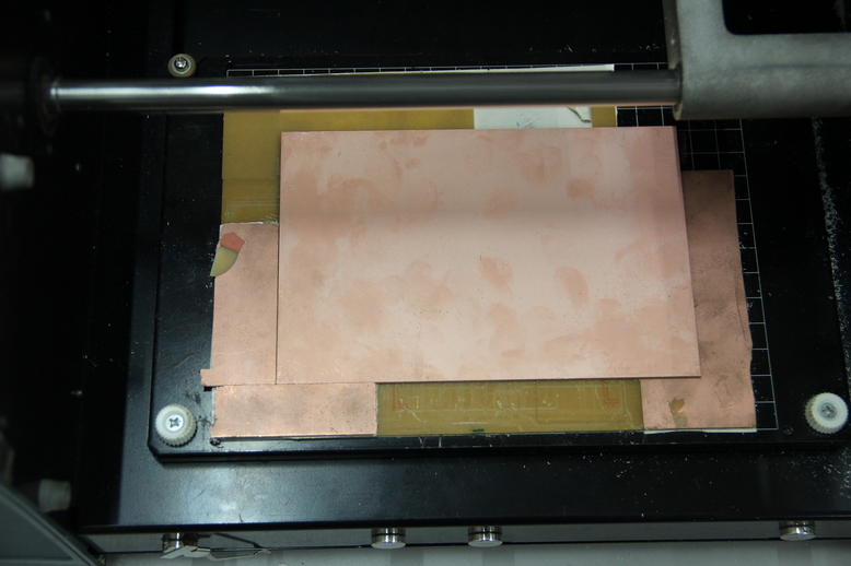
Milling Top Layer
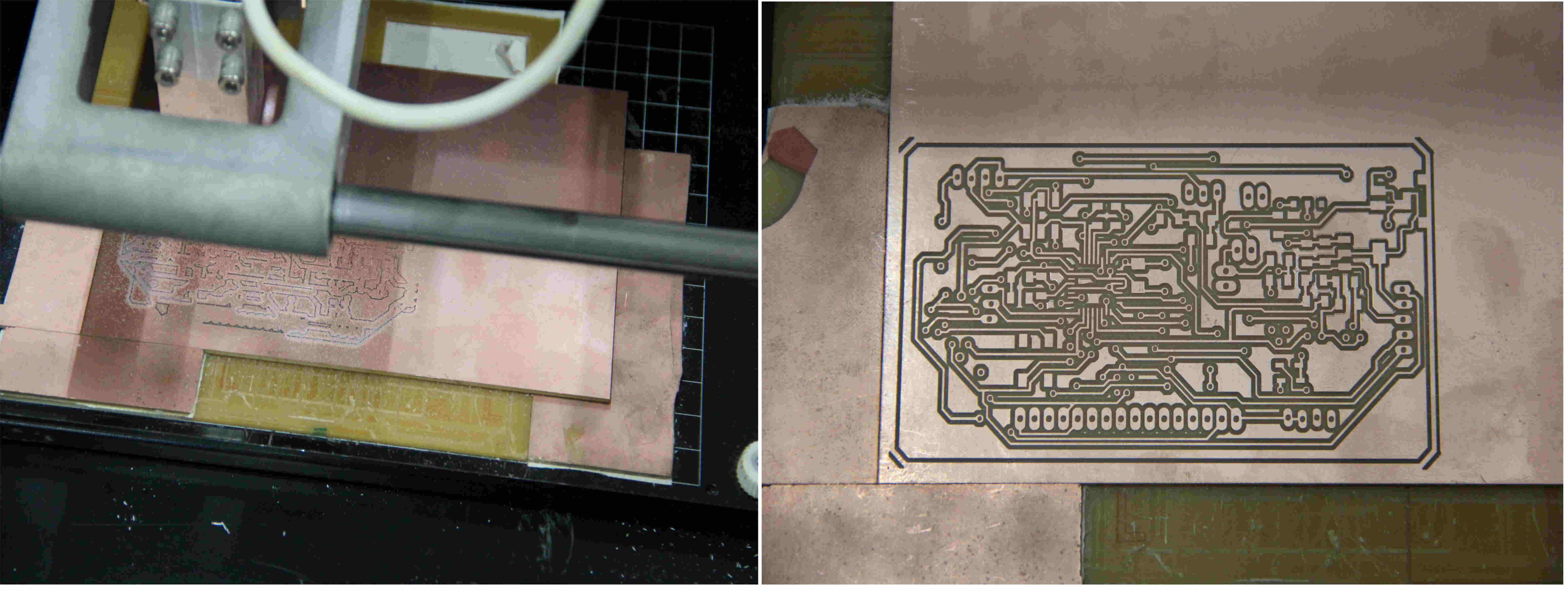
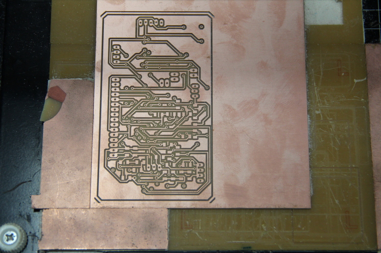
The top layer png image were opened in fab modules and milled the board using 1/64 (0.4mm) bit. The pcb milling of top layer and after the completion of toplayer is shown in the below image.
Milling bottom Layer
In this step i need to mill the bottom layer of the pcb, for that what i did is i flipped the bottom layer mill traces image horizontally and rotated it to 90 degree clockwise as shown below and like wise i placed the pcb on the bed of modela.
Drilling and cutting
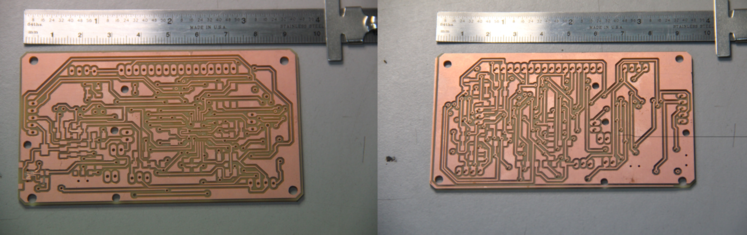
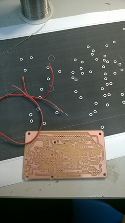
After milling the top and bottom layers, placed the top layer back on to the bed of modela. Then opened the cutout image(png) file in fab modules and changed the bit to 1/32mil(0.8mm) and processed. The final pcb after milling and cutting is given below. In this you can see that slight variations in the hole is there, but as it is very small i can adjust it. Some tarcks were shorted in the usb connector area due to the clearence issue. I seperated it using a knief.
The total Machine settings in fab modules are shown below. In cut path i have given the X origin 0.1mm lesser for just a correction factor but it didn't worked out.
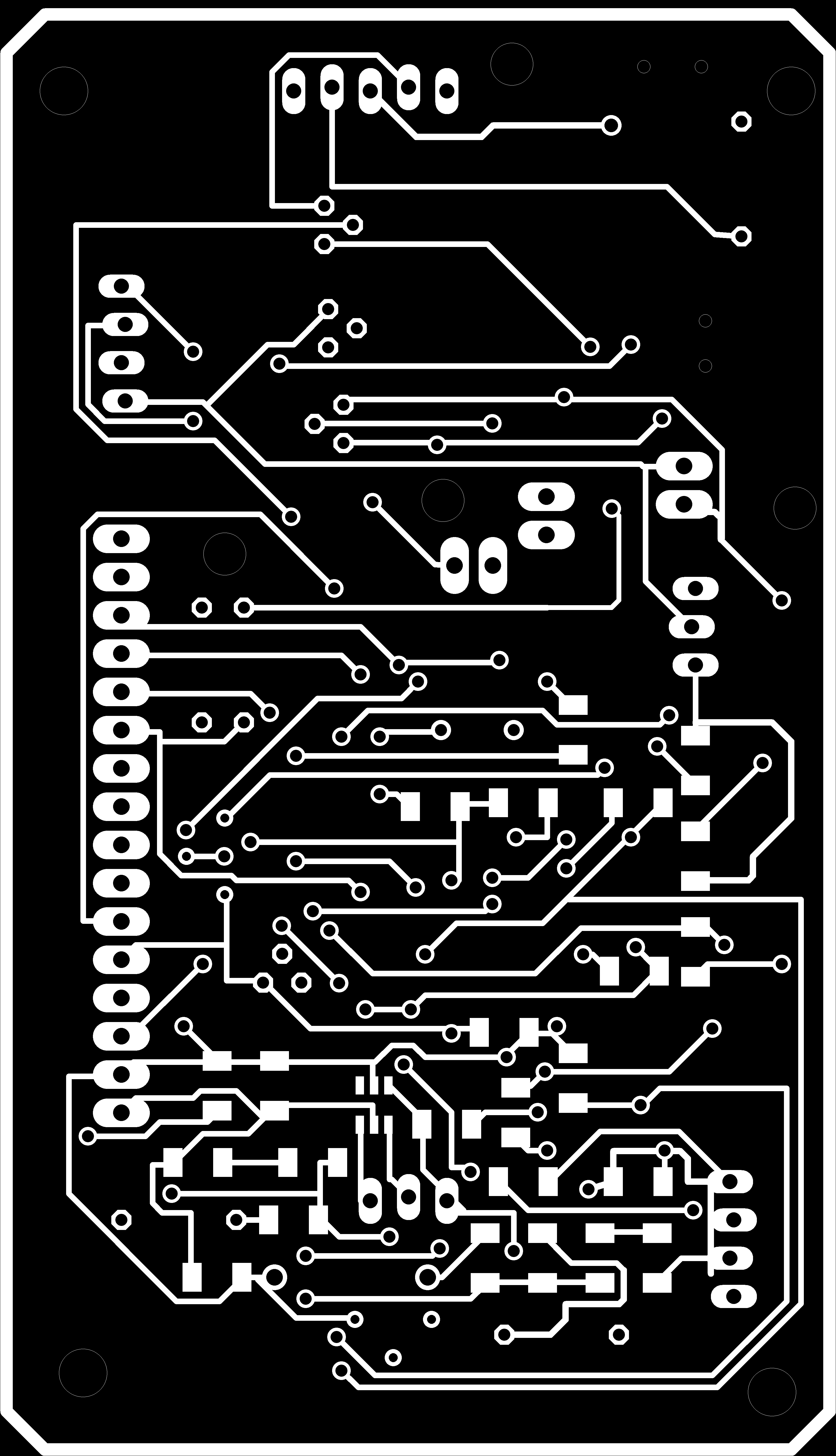
Final PCB
PCB Soldring
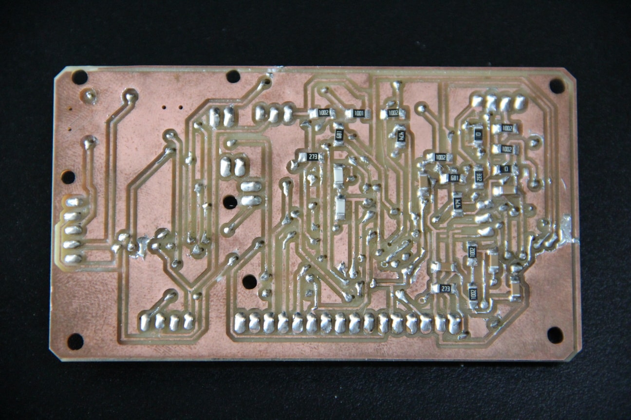
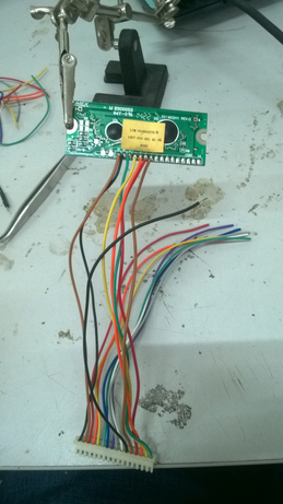
After completing the pcb milling, i did the via soldering . All the top and bottom traces were interconnected with vias and these vias need to be connected using wires. I have used multistranded wires for doing this from the ribbon cable available. Three starnds were taken and tinned using solder and placed in the via slot and slodered. It taken almost one day to finish the via soldering. You can export a via diagram from the board schematic in eagle and keep it for checking the vias, sometimes the via holes and leaded holes may give some confusions. Verifying the via diagram will save a lot of time.
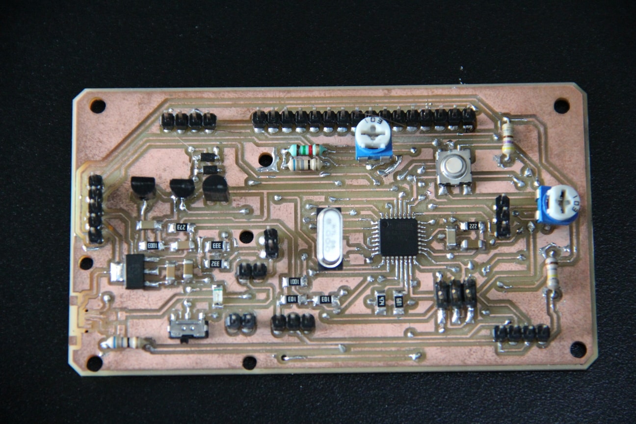
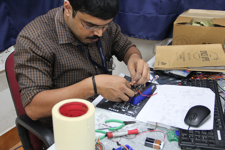
Next step after completing the via soldering is to solder the componenets on the pads. I divided the whole task into two batches because a few components was on shipment at that time. I planned to finish the soldering of the componenets which are available in the lab first, accordingly each parts were soldered. Since i required more componenets it was difficult for me to keep all components into a plate. Started soldering using weller soldering station and it took one more day to finish the complete soldering of first batch of componenets. The below showed image is the pcb after completing the vias and placed ATMEGA328P IC on the board.
First batch of components were successfully soldered into the board and by that time next batch is delivered and finished the soldering on the next day. It was a saturday night when i completed the soldering. I have used solder flux for soldering, all the flux particles were spattered on the board. I used isopropyl alcohol to clean all the board. The soldered PCB's are shown below.
Continuity checks
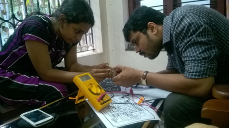
After first and second batch componenet soldering some pending componenets were there for soldering, i planned for doing a continuity check beacuse there are too many via connections and the tracks going top and botto layers, which is too closer and if any errors in the connection or soldering means i have to invest a lot time to find it, which will delays my shedules. Two person is required for doing this , One of my friend Mrs.Susmitha helped me to check the continuity using multimeter with the help of my pcb schematic and found some mistakes in GND connections, the summary is also showed here.
Summary of pcb continuity check
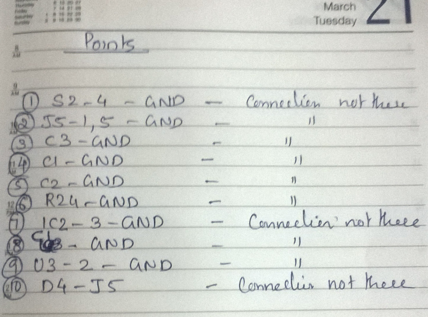
For correcting the issues, I have checked the layout and found that one via connection was not connected properly and is making all the GND connectivity isuues. Resoldered the point and the error got cleared. The below showed images are the heroshots of my easy tester pcb.
Embedded Programming & Testing of the Easy Tester
Ensured everything is correct and first i given the +9V battery to the J1 connector and checked the voltage regulator output using a multimeter and it showed +4.87V. Also checked the power is comming to all the VCC points on the board and it came correctly. Next to start with the program, i thought of going with C programming. Some open source programms were there and i have gone through and studied the logic, these are lengthy programms and i tried to program using avr dude and FabISP it showed errors. Later i have searched for some arduino version programs so that i cand edit easily. I found a Ardutester program using Arduino, gone through it deeply and learned the logic and edited the code accoring to my requirements. The total code is more than 9 pages and i am copying the starting few codes, you can download my full code on the bottom of this documentation.
Resistance Measurement
The measurement of a unknown resistor Rx is done in two ways with the build in precision 680Ω resistors. The test pin 1 (TP1) and test pin 3 (TP3) are used for this. In this the TP3 is connected to VCC and TP1 to GND . The direction of current flow through the resistor Rx is allways the same in both directions, because the sum of resistor values between VCC and GND is identical. In both configu- rations the value of resistor Rx can be computed with the known resistor values and the measured voltages, if the relation of resistor Rx and the 680Ω is not too high. For higher resistor values the measurements with the 470kΩ resistors are used. The mean value of both measurements is taken as displayed resistor value.The code for checking the resistance measurement is shown below.
- //Check for resistor
- void CheckResistor(void)
- {
- Resistor_Type *Resistor; //Pointer to resistor
- unsigned long Value1; //Resistance of measurement #1
- unsigned long Value2; //Resistance of measurement #2
- unsigned long Value; //Resistance value
- unsigned long Temp; //Temp. value
- signed char Scale; //Resistance scale
- signed char Scale2; //Resistance scale
- byte n; //Counter
- //Voltages
- unsigned int U_Rl_H; //Voltage #1
- unsigned int U_Ri_L; //Voltage #2
- unsigned int U_Rl_L; //Voltage #3
- unsigned int U_Ri_H; //Voltage #4
- unsigned int U_Rh_H; //Voltage #5
- unsigned int U_Rh_L; //Voltage #6
- wdt_reset(); //Reset watchdog
- /*
- Resistor measurement
- - Set up a voltage divider with well known probe resistors and
- measure the voltage at the DUT.
- - For low resistance consider the internal resistors of the µC
- for pulling up/down.
- - Calculate resistance via the total current and the voltage
- at the DUT.
- - We could also use the voltage divider rule:
- (Ra / Rb) = (Ua / Ub) -> Ra = Rb * (Ua / Ub)
- check if we got a resistor
- - A resistor has the same resistance in both directions.
- - We measure both directions with both probe resistors.
- */
- //We assume: resistor between probe-1 and probe-2, set probes: Gnd -- probe-2 / probe-1 -- Rl -- Vcc
- SetADCLow(); //Set ADC port low low
- ADC_DDR = Probes.ADC_2; //Pull down probe-2 directly
- R_DDR = Probes.Rl_1; //Enable Rl for probe-1
- R_PORT = Probes.Rl_1; //Pull up probe-1 via Rl
- U_Ri_L = ReadU_5ms(Probes.Pin_2); //Get voltage at internal R of µC
- U_Rl_H = ReadU(Probes.Pin_1); //Get voltage at Rl pulled up
- /*
Capacitor Measurement
The measurement of capacitor values are done as separate task by measurement of load time after all other measurements.You should always discharge the capacitor before connecting it to the tester. The tester additionally discharge the capacitor before any measurement. If the voltage is below 1300mV, the capacitor is shortened by the output pins of the connected ADC port (Port C).One side of the capacitor is connected to GND. The other side of the capacitor is connected with the 680Ω resistor to VCC for a period of 10ms. Afterwards this probe pin is switched to Input (High Impedance). After this 10 ms current pulse the voltage of the capacitor is measured without any current. If the voltage has not reached a minimal value of 300mV, the load pulse is repeated up to 499 times. If after 127 pulses a minimum voltage of 75mV is not reached (about 2s), further load is stopped, because never the 300mV can be reached with the remaining load pulses. The value of the capacity is then computed with the count of load pulses and the reached load voltage from a table. The table contains the factors to get the capacity in nF units from load time and the reached voltage with a spacing of 25mV.
- /*
- Calculate capacitance
- - use factor from pre-calculated LargeCap_table
- - ignore Config.CapZero since it's in the pF range
- */
- if (Flag == 3)
- {
- Scale = -9; //Factor is scaled to nF
- //Get interpolated factor from table
- Raw = GetFactor(U_Cap + U_Drop, TABLE_LARGE_CAP);
- Raw *= Pulses; //C = pulses * factor
- if (Mode & FLAG_10MS) Raw *= 10; // *10 for 10ms charging pulses
- if (Raw > UINT32_MAX / 1000) //Scale down if C >4.3mF
- {
- Raw /= 1000; //Scale down by 10^3
- Scale += 3; //Add 3 to the exponent
- }
- Value = Raw; //Copy raw value
- //It seems that we got a systematic error
- Value *= 100;
- if (Mode & FLAG_10MS) Value /= 109; //-9% for large cap
- else Value /= 104; //-4% for mid cap
- //Copy data
- Cap->A = Probes.Pin_2; //Pull-down probe pin
- Cap->B = Probes.Pin_1; //Pull-up probe pin
- Cap->Scale = Scale; //-9 or -6
- Cap->Raw = Raw;
- Cap->Value = Value; //Max. 4.3*10^6nF or 100*10^3µF
- }
- return Flag;
- }
- //Measure cap <4.7µF between two probe pins
- byte SmallCap(Capacitor_Type *Cap)
- {
- byte Flag = 3; //Return value
- byte TempByte; //Temp. value
- signed char Scale; //Capacitance scale
- unsigned int Ticks; //Timer counter
- unsigned int Ticks2; //Timer overflow counter
- unsigned int U_c; //Voltage of capacitor
- unsigned long Raw; //Raw capacitance value
- unsigned long Value; //Corrected capacitance value
- /*
- Measurement method used for small caps < 50uF:
- We need a much better resolution for the time measurement. Therefore we
- use the µCs internal 16-bit counter and analog comparator. The counter
- inceases until the comparator detects that the voltage of the DUT is as
- high as the internal bandgap reference. To support the higher time
- resolution we use the Rh probe resistor for charging.
- Remark:
- The analog comparator has an Input Leakage Current of -50nA up to 50nA
- at Vcc/2. The Input Offset is <10mV at Vcc/2.
- */
- Ticks2 = 0; //Reset timer overflow counter
- //Init hardware, prepare probes
- DischargeProbes(); //Try to discharge probes
- if (Check.Found == COMP_ERROR) return 0; //Skip on error
- //Set probes: Gnd -- all probes / Gnd -- Rh -- probe-1
- R_PORT = 0; //Set resistor port to low
- //Set ADC probe pins to output mode
- ADC_DDR = (1 << TP1) | (1 << TP2) | (1 << TP3);
- SetADCLow(); //Set ADC port to low
- R_DDR = Probes.Rh_1; //Pull-down probe-1 via Rh
- //Setup analog comparator
- ADCSRB = (1 << ACME); //Use ADC multiplexer as negative input
- ACSR = (1 << ACBG) | (1 << ACIC); //Use bandgap as positive input, trigger timer1
- ADMUX = (1 << REFS0) | Probes.Pin_1; //Switch ADC multiplexer to probe 1 and set AREF to Vcc
- ADCSRA = ADC_CLOCK_DIV; //Disable ADC, but keep clock dividers
- waitus(200);
- //Setup timer
- TCCR1A = 0; //Set default mode
- TCCR1B = 0; //Set more timer modes
- //Timer stopped, falling edge detection, noise canceler disabled
- TCNT1 = 0; //Set Counter1 to 0
- //Clear all flags (input capture, compare A & B, overflow
- TIFR1 = (1 << ICF1) | (1 << OCF1B) | (1 << OCF1A) | (1 << TOV1);
- R_PORT = Probes.Rh_1; //Pull-up probe-1 via Rh
- //Enable timer
- if (Check.Found == COMP_FET)
- {
- //Keep all probe pins pulled down but probe-1
- TempByte = (((1 << TP1) | (1 << TP2) | (1 << TP3)) & ~(1 << Probes.Pin_1));
- }
- else
- {
- TempByte = Probes.ADC_2; //Keep just probe-1 pulled down
- }
- //Start timer by setting clock prescaler (1/1 clock divider)
- TCCR1B = (1 << CS10);
- ADC_DDR = TempByte; //Start charging DUT
- //Timer loop - run until voltage is reached - detect timer overflows
- while (1)
- {
- TempByte = TIFR1; //Get timer1 flags
- //End loop if input capture flag is set (= same voltage)
- if (TempByte & (1 << ICF1)) break;
- //Detect timer overflow by checking the overflow flag
- if (TempByte & (1 << TOV1))
- {
- //Happens at 65.536ms for 1MHz or 8.192ms for 8MHz
- TIFR1 = (1 << TOV1); //Reset flag
- wdt_reset(); //Reset watchdog
- Ticks2++; //Increase overflow counter
- //End loop if charging takes too long (13.1s)
- if (Ticks2 == (CPU_FREQ / 5000)) break;
- }
- }
- //Stop counter
- TCCR1B = 0; //Stop timer
- TIFR1 = (1 << ICF1); //Reset Input Capture flag
- Ticks = ICR1; //Get counter value
- //Disable charging
- R_DDR = 0; //Set resistor port to HiZ mode
- //Catch missed timer overflow
- if ((TCNT1 > Ticks) && (TempByte & (1 << TOV1)))
- {
- TIFR1 = (1 << TOV1); //Reset overflow flag
- Ticks2++; //Increase overflow counter
- }
- //Enable ADC again
- ADCSRA = (1 << ADEN) | (1 << ADIF) | ADC_CLOCK_DIV;
- //Get voltage of DUT
- U_c = ReadU(Probes.Pin_1); //Get voltage of cap
- //Start discharging DUT
- R_PORT = 0; //Pull down probe-2 via Rh
- R_DDR = Probes.Rh_1; //Enable Rh for probe-1 again
- //Skip measurement if charging took too long
- if (Ticks2 >= (CPU_FREQ / 5000)) Flag = 1;
- //Calculate capacitance (<50uF) - use factor from pre-calculated SmallCap_table
- if (Flag == 3)
- {
- //Combine both counter values
- Raw = (unsigned long)Ticks; //Set lower 16 bits
- Raw |= (unsigned long)Ticks2 << 16; //Set upper 16 bits
- if (Raw > 2) Raw -= 2; //Subtract processing time overhead
- Scale = -12; //Default factor is for pF scale
- if (Raw > (UINT32_MAX / 1000)) //Prevent overflow (4.3*10^6)
- {
- Raw /= 1000; //Scale down by 10^3
- Scale += 3; //Add 3 to the exponent (nF)
- }
- //Multiply with factor from table
- Raw *= GetFactor(Config.U_Bandgap + Config.CompOffset, TABLE_SMALL_CAP);
- //Divide by CPU frequency to get the time and multiply with table scale
- Raw /= (CPU_FREQ / 10000);
- Value = Raw; //Take raw value
- //Take care about zero offset if feasable
- if (Scale == -12) //pF scale
- {
- if (Value >= Config.CapZero) //If value is larger than offset
- {
- Value -= Config.CapZero; //Substract offset
- }
- else //If value is smaller than offset
- {
- //We have to prevent a negative value
- Value = 0; //Set value to 0
- }
- }
- //Copy data
- Cap->A = Probes.Pin_2; //Pull-down probe pin
- Cap->B = Probes.Pin_1; //Pull-up probe pin
- Cap->Scale = Scale; //-12 or -9
- Cap->Raw = Raw;
- Cap->Value = Value; //Max. 5.1*10^6pF or 125*10^3nF
- /*
- Self-adjust the voltage offset of the analog comparator and internal
- bandgap reference if C is 100nF up to 20µF. The minimum of 100nF
- should keep the voltage stable long enough for the measurements.
- Changed offsets will be used in next test run.
- */
- if (((Scale == -12) && (Value >= 100000)) ||
- ((Scale == -9) && (Value <= 20000)))
- {
- signed int Offset;
- signed long TempLong;
- /*
- * We can self-adjust the offset of the internal bandgap reference
- by measuring a voltage lower than the bandgap reference, one time
- with the bandgap as reference and a second time with Vcc as
- reference. The common voltage source is the cap we just measured.
- */
- while (ReadU(Probes.Pin_1) > 980)
- {
- //Keep discharging
- }
- R_DDR = 0; //Stop discharging
- Config.AutoScale = 0; //Disable auto scaling
- Ticks = ReadU(Probes.Pin_1); //U_c with Vcc reference
- Config.AutoScale = 1; //Enable auto scaling again
- Ticks2 = ReadU(Probes.Pin_1); //U_c with bandgap reference
- R_DDR = Probes.Rh_1; //Resume discharging
- Offset = Ticks - Ticks2;
- //Allow some offset caused by the different voltage resolutions (4.88 vs. 1.07)
- if ((Offset < -4) || (Offset > 4)) //Offset too large
- {
- /*
- Calculate total offset:
- - first get offset per mV: Offset / U_c
- - total offset for U_ref: (Offset / U_c) * U_ref
- */
- TempLong = Offset;
- TempLong *= Config.U_Bandgap; // * U_ref
- TempLong /= Ticks2; // / U_c
- Config.RefOffset = (signed char)TempLong;
- }
- /*
- In the cap measurement above the analog comparator compared
- the voltages of the cap and the bandgap reference. Since the µC
- has an internal voltage drop for the bandgap reference the
- µC used actually U_bandgap - U_offset. We get that offset by
- comparing the bandgap reference with the voltage of the cap:
- U_c = U_bandgap - U_offset -> U_offset = U_c - U_bandgap
- */
- Offset = U_c - Config.U_Bandgap;
- //Limit offset to a valid range of -50mV - 50mV
- if ((Offset > -50) && (Offset < 50)) Config.CompOffset = Offset;
- }
- }
- return Flag;
- }
Diode Measurement
The code for measurement of diode is showed below. In this first it will sense the diodes and displays the diode symbol cathode anode with its pin numbers. Also it will checks the capacitance of the diode. The programm will automatically detect different cutin voltages.
- //Display Uf of a diode
- void ShowDiode_Uf(Diode_Type *Diode)
- {
- //Sanity check
- if (Diode == NULL) return;
- //Display Vf
- DisplayValue(Diode->V_f, -3, 'V');
- }
- //Display capacitance of a diode
- void ShowDiode_C(Diode_Type *Diode)
- {
- //Sanity check
- if (Diode == NULL) return;
- //Get capacitance (opposite of flow direction)
- MeasureCap(Diode->C, Diode->A, 0);
- //And show capacitance
- DisplayValue(Caps[0].Value, Caps[0].Scale, 'F');
- }
- //Show diode
- void ShowDiode(void)
- {
- Diode_Type *D1; //Pointer to diode #1
- Diode_Type *D2 = NULL; //Pointer to diode #2
- byte SkipFlag = 0; //Flag for anti-parallel diodes
- byte A = 5; //ID of common anode
- byte C = 5; //ID of common cothode
- unsigned int I_leak; //Leakage current
- D1 = &Diodes[0]; //Pointer to first diode
- //Figure out which diodes to display
- if (Check.Diodes == 1) //Single diode
- {
- C = D1->C; //Make anode first pin
- }
- else if (Check.Diodes == 2) //Two diodes
- {
- D2 = D1;
- D2++; //Pointer to second diode
- if (D1->A == D2->A) //Common anode
- {
- A = D1->A; //Save common anode
- }
- else if (D1->C == D2->C) //Common cathode
- {
- C = D1->C; //Save common cathode
- }
- //Anti-parallel
- else if ((D1->A == D2->C) && (D1->C == D2->A))
- {
- A = D1->A; //Anode and cathode
- C = A; //Are the same
- SkipFlag = 1; //Signal anti-parallel diodes
- }
- }
- else if (Check.Diodes == 3) //Three diodes
- {
- byte n;
- byte m;
- /*
- Two diodes in series are additionally detected as third big diode:
- - Check for any possible way of 2 diodes be connected in series.
- - Only once the cathode of diode #1 matches the anode of diode #2.
- */
- for (n = 0; n <= 2; n++) //Loop for first diode
- {
- D1 = &Diodes[n]; //Get pointer of first diode
- for (m = 0; m <= 2; m++) //Loop for second diode
- {
- D2 = &Diodes[m]; //Get pointer of second diode
- if (n != m) //Don't check same diode :-)
- {
- if (D1->C == D2->A) //Got match
- {
- n = 5; //End loops
- m = 5;
- }
- }
- }
- }
- if (n < 5) D2 = NULL; //No match found
- C = D1->C; //Cathode of first diode
- A = 3; //In series mode
- }
- else //To much diodes
- {
- D1 = NULL; //Don't display any diode
- ShowFail(); //And tell user
- return;
- }
- //Display pins, first Diode
- if (A < 3) lcd_testpin(D1->C); //Common anode
- else lcd_testpin(D1->A); //Common cathode
- if (A < 3) lcd_fixed_string(Diode_CA_str); //Common anode
- else lcd_fixed_string(Diode_AC_str); //Common cathode
- if (A < 3) lcd_testpin(A); //Common anode
- else lcd_testpin(C); //Common cathode
- if (D2) //Second diode
- {
- if (A <= 3) lcd_fixed_string(Diode_AC_str); //Common anode or in series
- else lcd_fixed_string(Diode_CA_str); //Common cathode
- if (A == C) lcd_testpin(D2->A); //Anti parallel
- else if (A <= 3) lcd_testpin(D2->C); //Common anode or in series
- else lcd_testpin(D2->A); //Common cathode
- }
- /*
- display:
- - Uf (forward voltage)
- - reverse leakage current (for single diodes)
- - capacitance (not for anti-parallel diodes)
- */
- //Uf
- lcd_line(2); //Go to line #2
- lcd_fixed_string(Vf_str); //Display: Vf=
- ShowDiode_Uf(D1); //First diode
- lcd_space();
- if (D2 == NULL) //Single diode
- {
- //Display low current Uf if it's quite low (Ge/Schottky diode)
- if (D1->V_f2 < 250)
- {
- lcd_data('(');
- DisplayValue(D1->V_f2, 0, 0);
- lcd_data(')');
- }
- //Reverse leakage current
- UpdateProbes(D1->C, D1->A, 0); //Reverse diode
- I_leak = GetLeakageCurrent(); //Get current (in µA)
- if (I_leak > 0) //Show if not zero
- {
- #ifdef BUTTON_INST
- TestKey(USER_WAIT, 11); //Next page
- #else
- delay(3000);
- #endif
- lcd_clear_line(2); //Only change line #2
- lcd_fixed_string(I_R_str); //Display: I_R=
- DisplayValue(I_leak, -6, 'A'); //Display current
- }
- }
- else
- {
- ShowDiode_Uf(D2); //Second diode (optional)
- }
- //Capacitance
- if (SkipFlag == 0)
- {
- #ifdef BUTTON_INST
- TestKey(USER_WAIT, 11); //Next page
- #else
- delay(3000);
- #endif
- lcd_clear_line(2); //Only change line #2
- lcd_fixed_string(DiodeCap_str); //Display: C=
- ShowDiode_C(D1); //First diode
- lcd_space();
- ShowDiode_C(D2); //Second diode (optional)
- }
- }
Like this each and every componenet is being measured and displayed to the LCD display. all the configuration values are stored in EEPROM
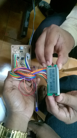
For programming i used fabisp and through arduino IDE flashed the program into the easy tester board. Next i soldered the Lumex 16X2 LCD available in our lab using a 16X1 header connector and connected to J5-LCD interface connector. I was little bit tensed during programming and missed some snaps in between, After connecting the LCD i connected the battery and suddenly the diplay came but the brightness was too low . I adjusted the potentiometer attached to the VEE point of the LCD and now the brightness became normal, It showed "FAB SM V.0.0" on the top row and my name on the bottom row. FAB SM V 0.0 was the name i intially given for my project. The initial test result is shown below.
Next i connected the push button switches other connections in bread board and tested with the componenets and it started showing the resistance and other device measurements.
Download Easy Tester program files (.zip)
II. Mechanical Design
Mechanical case
I started the design of the case after routing of my pcb, the pcb is the space consuming item in my case. While doing the milling i started the mechanical design in Rhinocerous. The total mechanical parts are divided into four parts.
- Bottom cover
- Top cover
- Slide cap
- probe
Bottom Cover
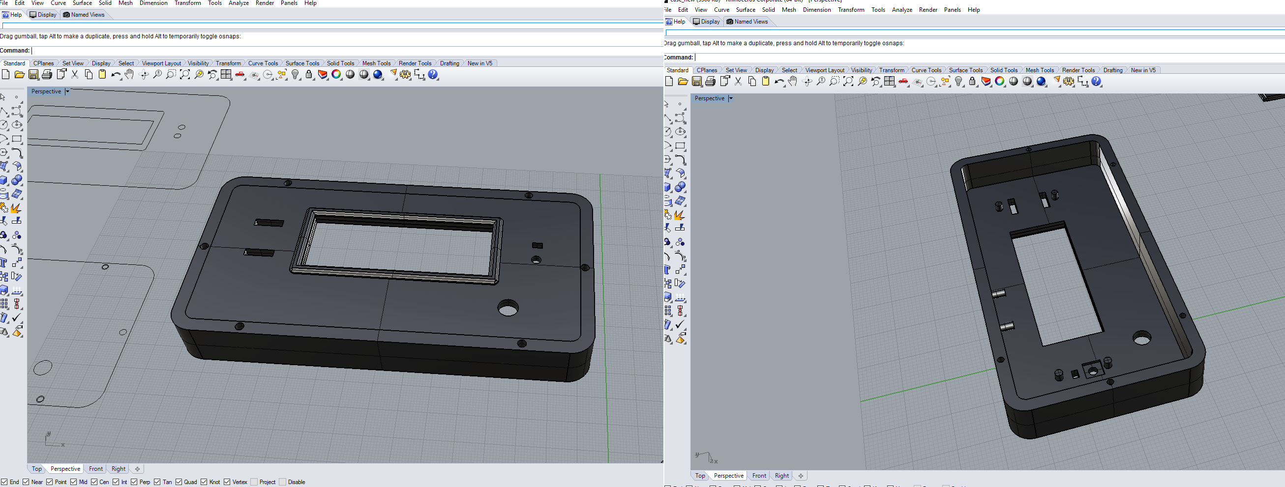
I started with bottom cover design, In this i planned to keep the main pcb, prode jacks, connectors and the battery. Exported the dimension of my pcb from eagle to dxf format and imported into rhinocerous. Actually i have put mounting holes on the pcb to mount it on the base of the bottom cover, to design these mounting holes in the correct position will not be that much easy in rhino. The exported file in rhino and the base part top view with dimension is shown below.
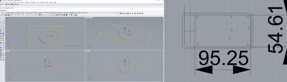
Exported the mounting holes like the pillers and supporting structures were given to the side walls of the case. I planned to put the portable probes for the measurement of SMD componenets from the side wall and on the next side i planned the connectors for external programming and for the serial communication connectors. Finally my bottom cover part is ready.
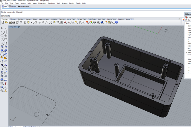
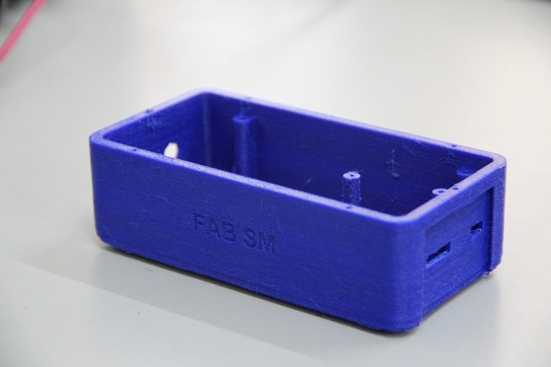
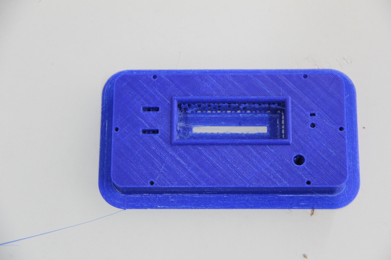
The file was exported in stl format to be printed in Ultimaker 3D printer, sliced using cura software and printed using blue PLA material. The 3D printed part is shown below.
Top Cover
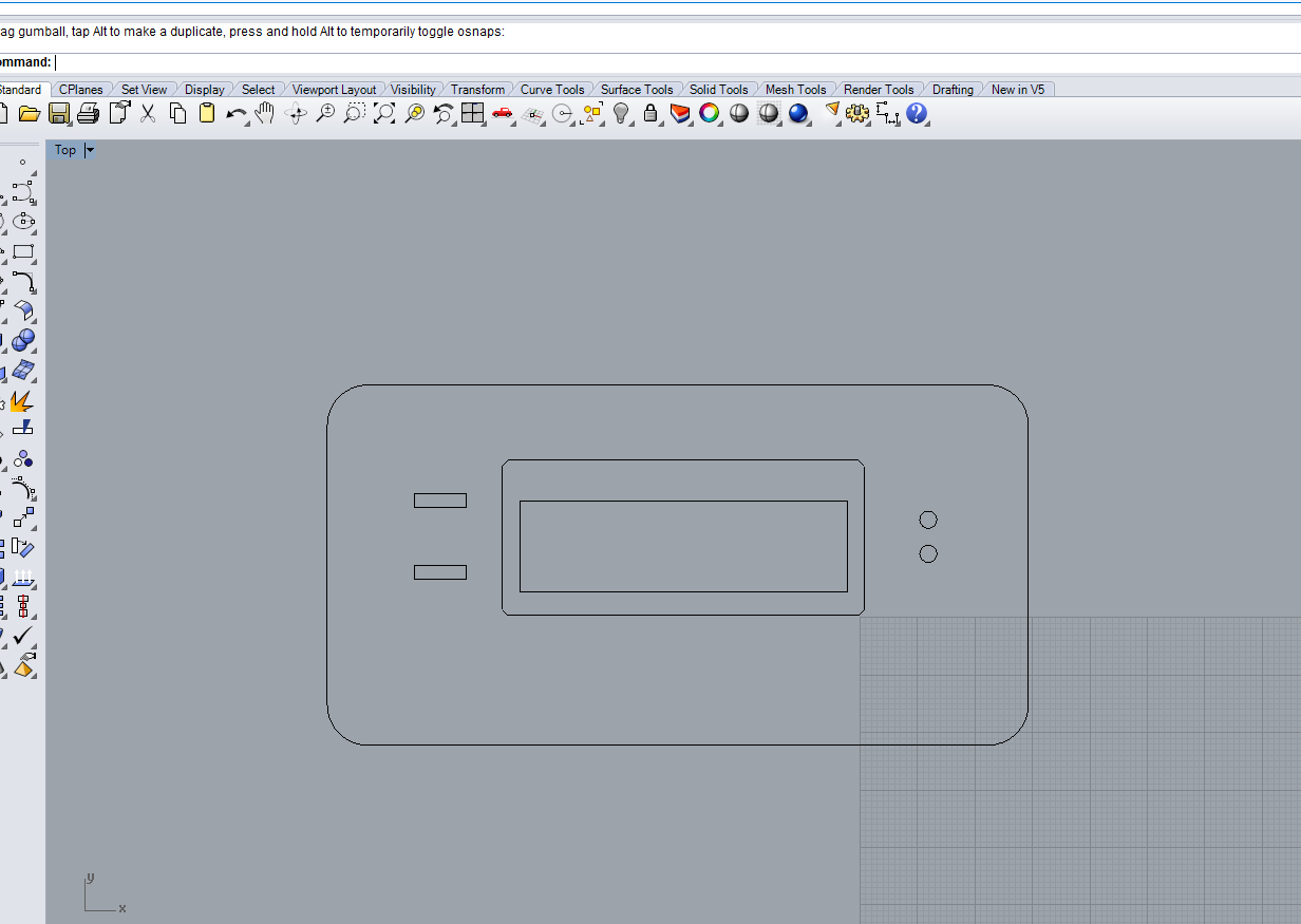
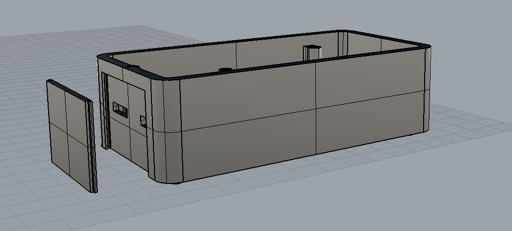
Top cover portion design is done based on the dimension of bottom cover. In my bottom cover i have given holes for screwing the topcover into the bottom cover of 2mm diameter. Given the slots for fixing the LCD panel, the dimensions of it are taken manually from the LCD. Etra slots were given for placing the switches , push button switches, LED and Rotary encoder. All the dimensions were physically measured and deigned. The initial sketch anf final part of Top cover is shown below.
Final top cover design top and botton views are showed below.
The file was exported into stl format and printed in ultimaker in same PLA color material which is shown below.
Slide cap
Slide cap is a cover for the two sides of the bottom cover, it is easily detached from the case. The design i inspired from our Digital vernier scale battery cap, as it is simple in design and functionally strong. I made a slot on the side wals to sliding the cap. The slide cap design is shown below.
Probe
My next plan is to make a portable probe for the measurement of SMD componenets. The probe can be connected to the female slot planned in the side wall of the bottom cover. Many ideas came into mind, first i thought of making a plastic casted probe or laser cutted one etc.. but later i understood that the probe should be little flexible and strong. If i made the probe in plastic casting it will be rigid and will easily break while measuring smd componenets. Next i thought to make a flexible probe, done some design tests with 3D printer. Actually the plan is to make it flexible but the dimensions were too small and it sticked at the time of 3D printing. Later I decided to make the probe using the same design but not fully flexible.
The design of my probe to be 3D printed is shown below. In head portion i have extruded the 3D design of fab lab logo and placed as the key logo of my probe.
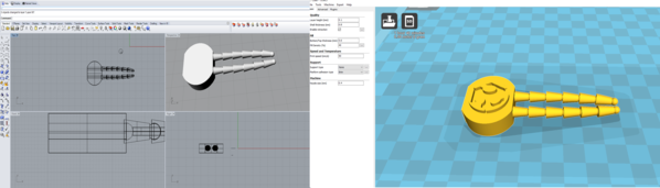
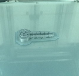
3D printed probe
Production file Downloads
Download Easy Tester case production files(STL) (.zip)
Download Easy Tester 3D Design files(STL) (.zip)
III. Integration
Integration is assembling all the mechanical and electrical parts to gather inside the case. The total integration part is divided into four different parts.
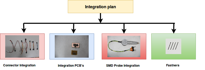
- Connector Integration
- Integration pcb's
- SMD portable probe integration
- Mechanical fastners
Conector Integration
There are total 9 connectors available in my board i need to route these connectors to different parts in the system. I have made mating connectors using ribbon cables with different lengths according to the routing direction. All connectors were terminated using header pins with heat shrinkable sleeves as shown below.
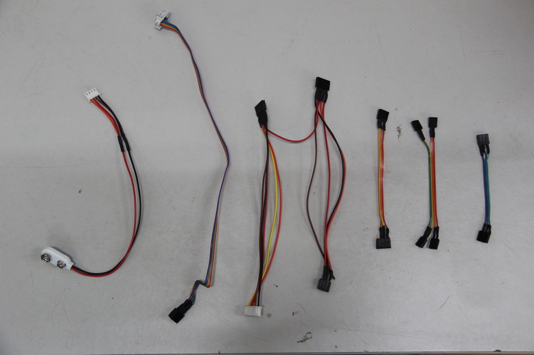
for LCD integration i have bought female header cables from the local market and soldered it into the LCD pins according to the connector detailes provided above.
Integration PCB's
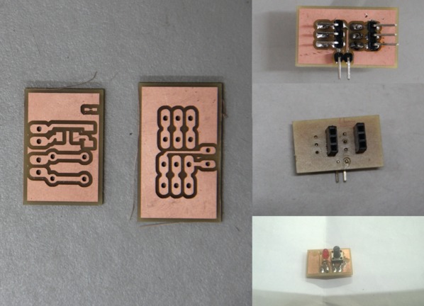
Integration pcb's are provided to interconnect the actual physical parts such as push buttons, rotary encoders , led displays, probe connections and other external connectors. I have made two pcb's one for connecting the LED and push button to the front panel and the other for connecting the test probe pins TP1 and TP2. All these two boards were designed using eagle software routed and processed in modela and made the board processes is shown below.
Pcb for Push button and LED
I have given the lable for this pcb as SM-B2, It is a holder for LED and a push button terminated in connector pins.
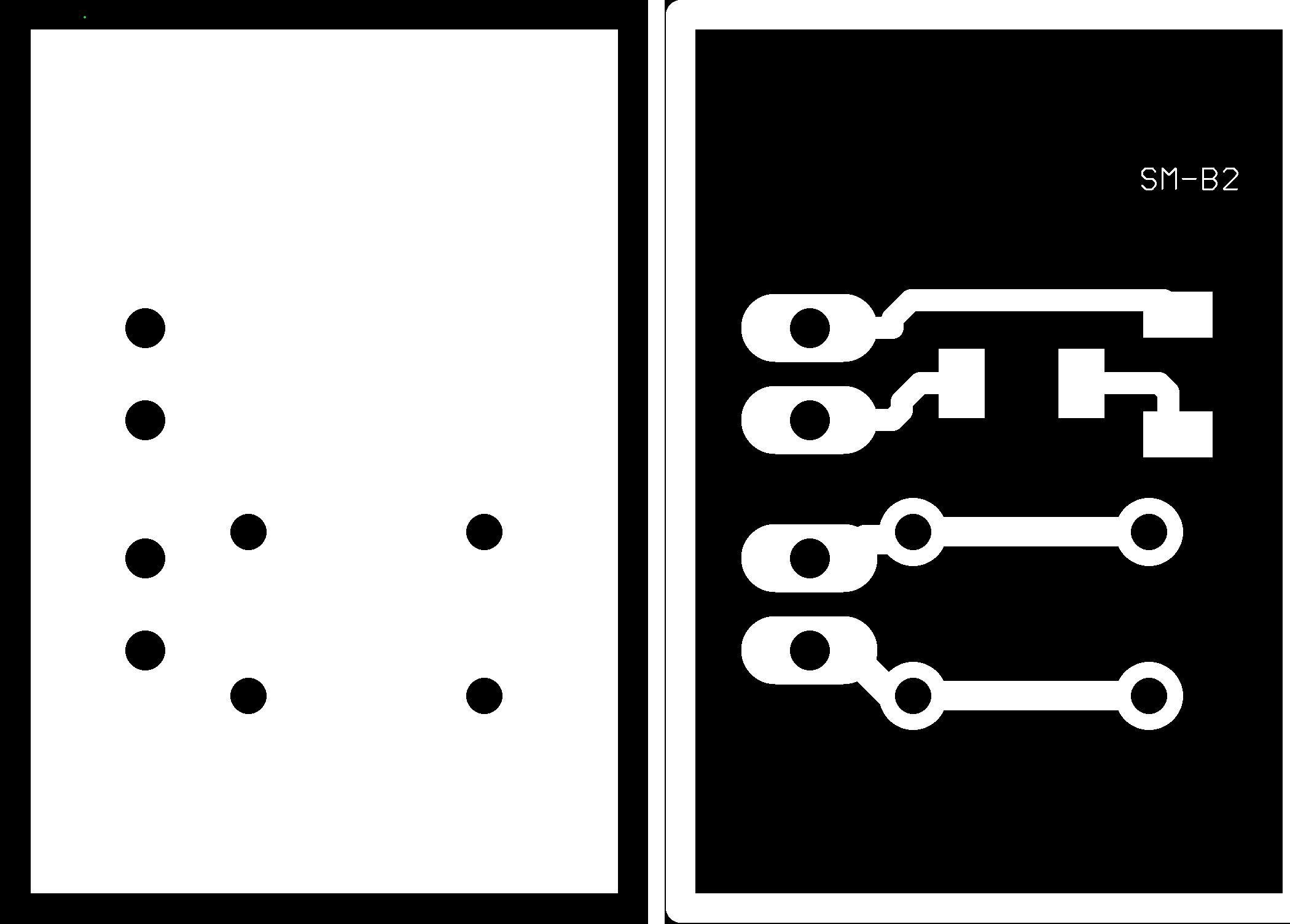
Test probe pcb
Test probe pcb is used to connect the test probe pin TP1, TP2 to the top cover and to the portable probe jacks on the case side.
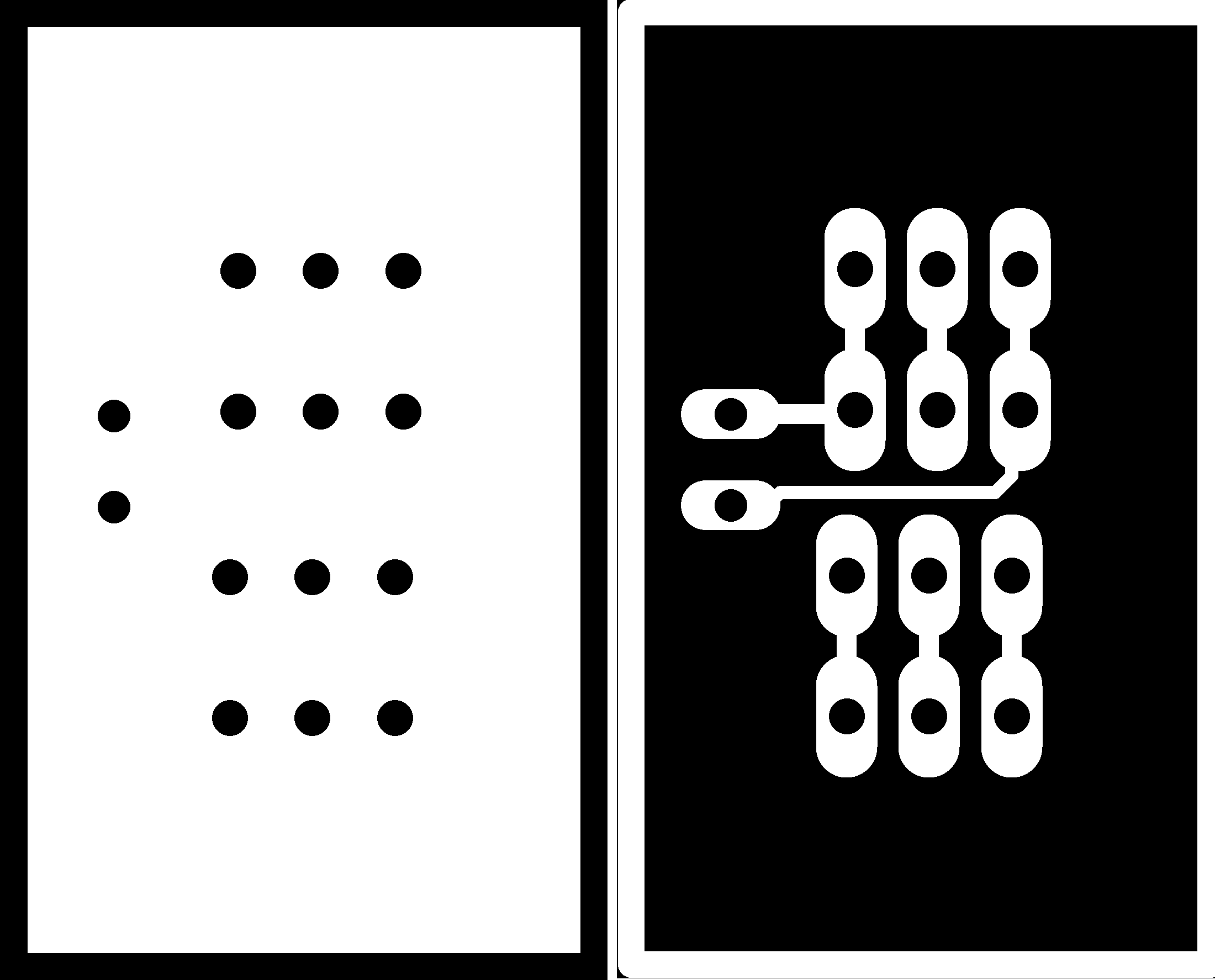
Final integration pcb's after milling and soldering is shown below.
SMD probe integration
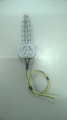
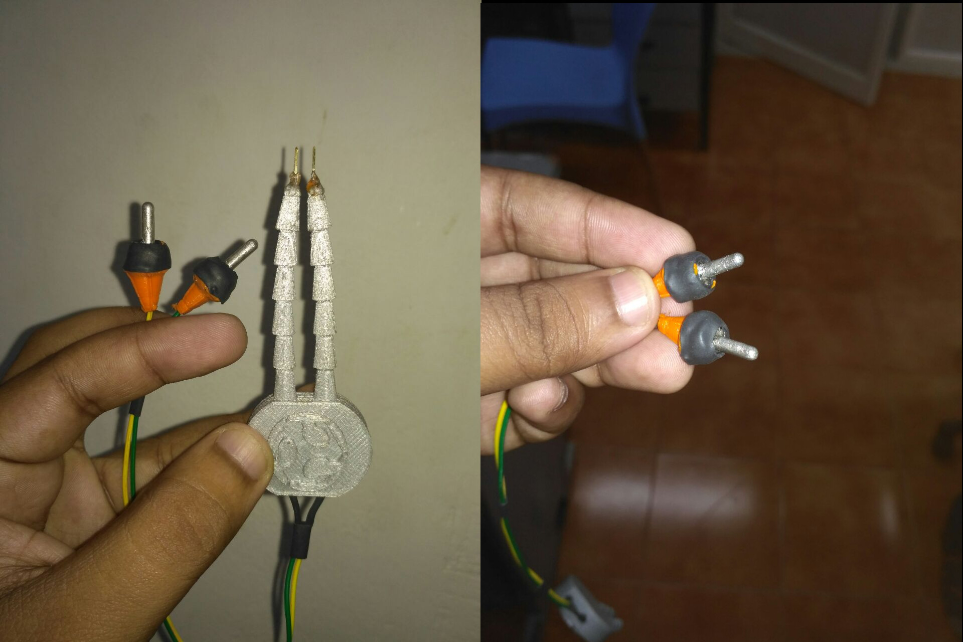
I made a 3d printed probe for checking the SMD devices, for that the connections have to be taken and have to be terminated in the jacks. I have used the copper wire available in the the lab, used as the wire for the probe inside the 3d printed probe. Two such copper wires are given parallely on each probe inorder to compensate the errors due to the probe resistance. The tip of the probe i have soldered a male header pin and in the other end i have to connect a male jack.
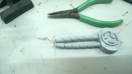
SMD probe after soldering the tips and jack wires is shown below.
Metal casting of jacks
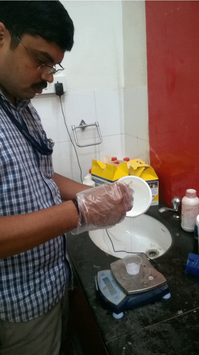
Inorder to terminate the wires from the probe i needed a jack , which will finally connect to the test probes. In fab inventory i fund one male jack, but the open flange and the size was too bigger and won't suit to my probe female pins. Then i need to place my connectors projecting outside of the wall and that will not look good for my tester. So i planned to go with metal casted probes, for that i used the same jack as the mould and placed inside a cup and poured with liquid silicone rubber compound (LSR1) which i have used earlier in the moulding and casting week.
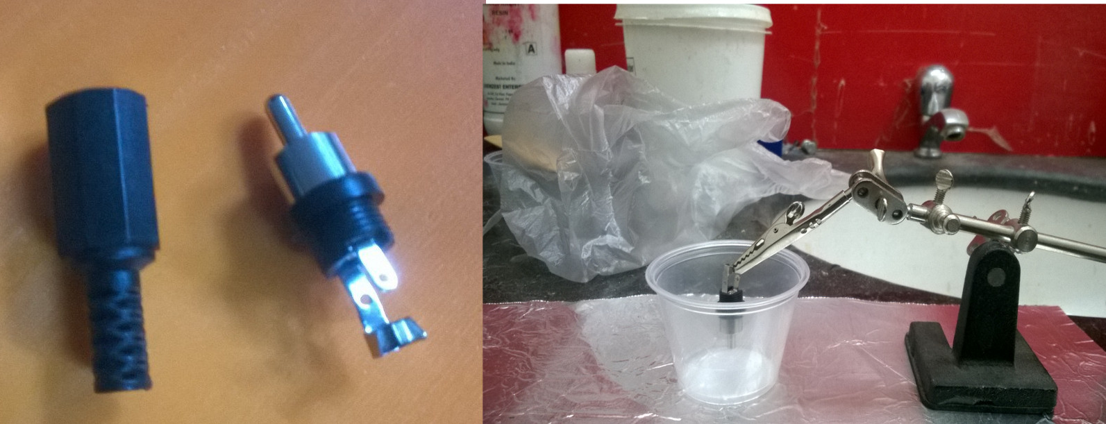
The LSR1 Part A and Part B were mixed in 100:10 proportion and pured into the setup carefully and slowly. Here i am showing the gif of silicone casting.
Next is casting the metal into the mould, we have babbit metal available in the lab. Some small pieces were there i had taken those pieces and put into the crusible and using the furnace, melted the metal and poured into the crucible. Babit metal will melt on around 200 degree centigrade, i have given aroung 400 degree. You can see in the below figure that it didn't worked out because the size of the head was too small so due to air trapping it didn't come correctly.
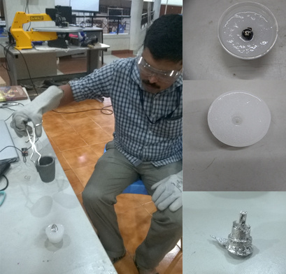
Then i have done the same thing with soldering station, as the babit metal will melt above 200 degrees i tried this. The result was positive, used the casted metal piece and i made the probe jack as shown in the image.
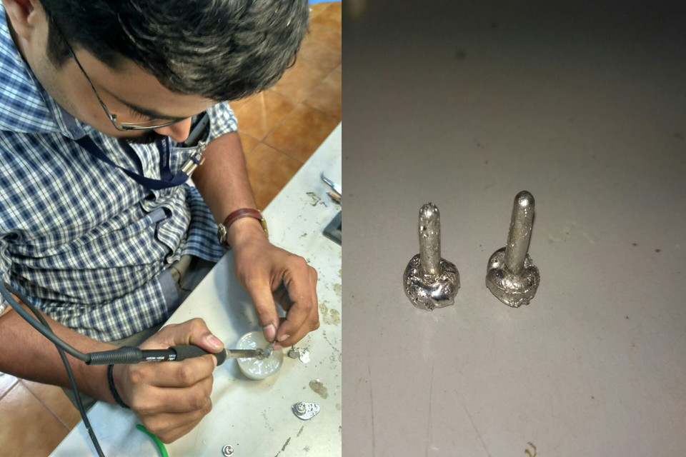
The finish was good enough , and i soldered the probe wires directly into the jack tips just casted and put the sleeve and made a cap cover for it in rhino and 3D printed with orange PLA. The tip heads is covered using heat shrinkable sleeves and it looks good.

Mechanical fastners
I have used M3X6mm screws with washer for fixing the pcb to the bottom case. Top cover to the bottom case can be fixed using M2X30mm screws.
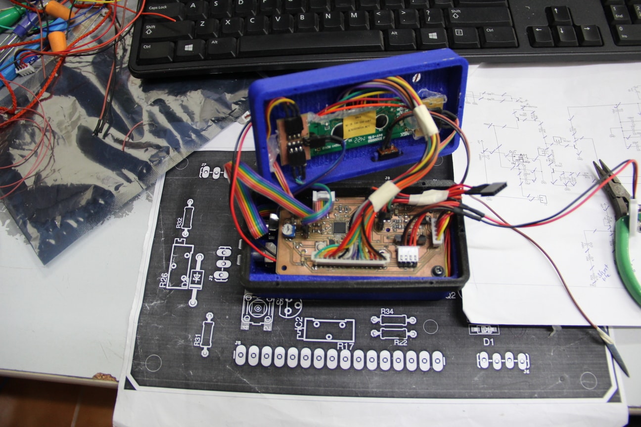
Integration
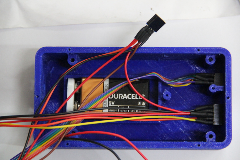
Connected all the connectors and pcb using the connectro mapping. First i assembled the base cover , in the bottom cover placed the battery and on the top mounted the main pcb with screws and then connected all other connectors. Two female connector jacks were connected on the side wall of the case and the connections were taken to the pcb.
After connecting i faced one issue that my top cover is not having enough clearence, due to the connector cables. The topcover didn't getting closed with the bottom case. Inoreder to clear this issue i made a extra strip on the same dimension as the bottom cover but having 10mm height on rhinocerous and printed. This will be placed like a spacer in between the top cover and bottom case. 3D printed the spacer in black color for matching with blue color and assembled. The integration pcbs were fixed on the respective slots and applied hot glue. You can see the final top assembly and the whole assembly part.
Final Testing
Once the assembly is over i turned on the tester with the slide switch attached on the topcover and the red LED started, currently i am configured the easy tester to work in normal mode i have connected the led through a 470ohm resistor in series with the battery line. The LCD worked perfectly, then i tried to test different passive and active componenets and it showed the reading correctly. Then moved to test the SMD componenets with the probe i made, Some connection issue was there and i corrected it and then using the probe i was able to test the SMD resistors,LED's and capacitors. I am skipping the output videos here because in the bottom i will show you the video output from my easy tester.
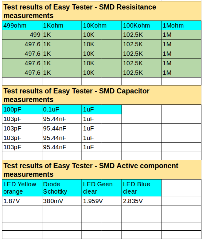
The test results from my Easy tester for different componenets is showed below. I have done this using the SMD portable probe, used the componenets from the inventory and later tabulated in Excel sheet.
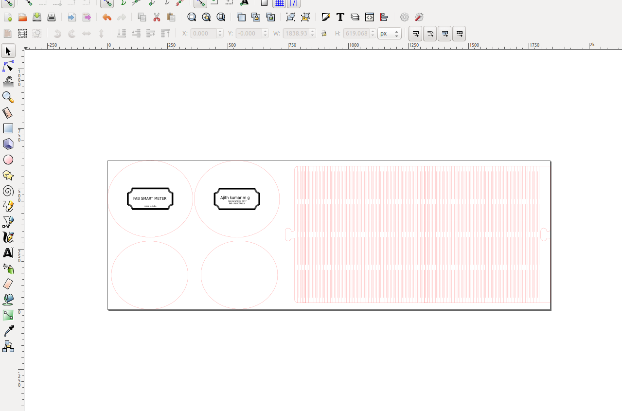
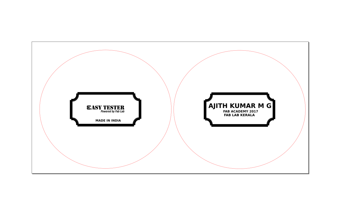
Vinyl Stickering
Next moved to cut some sticker cutting on vinyl machine, i have designed a easy tester logo in gimp and exported into png format and processed using vinyl cutter. The main attraction i have given to this is the middle portion of the letter "E" is an arrow which is a inward arrow, shows the symbolic representation of plugging the componenets. Used different colors for the stickering to give attraction to the unit than a single color.

Next i have downloaded the image of slide to open image from internet to put on the slide cap. The image was opened in inkscape and converted into bitmap and cut using vinyl cutter. The settings and operation are same as we did in computer controlled cutting week. Also the label for push button was given as Strat and the two test ports are labeled TP1 nad TP2 are also cutted using the vinyl cutter.

I also planned to cover the top of the easy tester box with black color vinyl sheet, for that i exported the top cover dimension file from rhino and edited in Inkscape and processed in vinyl machine with black colored sticker. Over the sticker i pasted all other labels. I deleted the rotary encoder hole from the design, as i thought to implement it in future.

Everything is ready now and assembly heroshot is shown below.
Download the Vinyl cutting files(.zip)
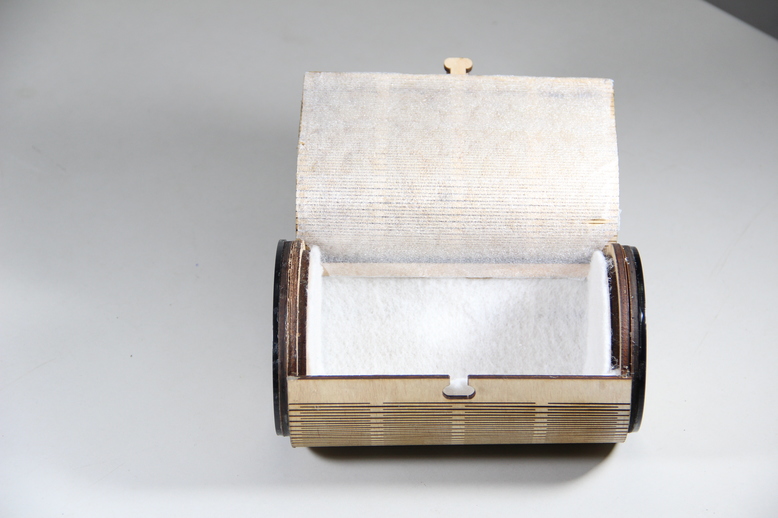
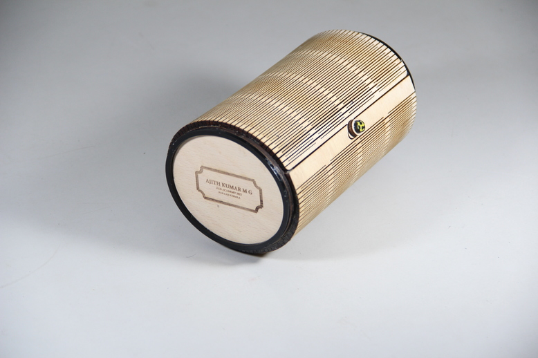
Carry case box for Easy Tester
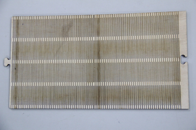
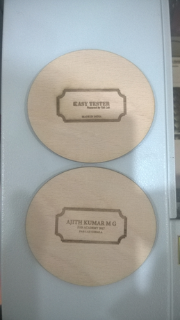
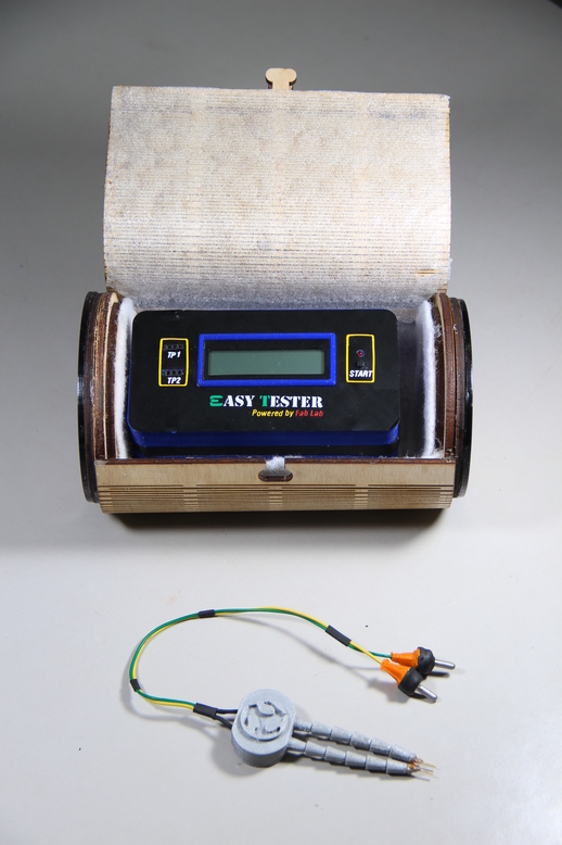
I planned to make a carry case for my easy tester, as i have seen that the standard products in the market will have its own attractive carry cases. Several design ideas came into my mind, i thought of making a flexture case in wood. In computer controlled week i had done sone flexture tests based on that i planned a design to make the box. The design is drwan in rhinocerous and exported to dxf file format and cutted in 4mm ply wood sheet and made the box The design filles and final integrated box are shown below. It is having an oval shape the two sides is having two layers of different sizes. Intially the name i was given as Fab smart meter and later i made one more plate and pasted over it. Now total three layers are there in each side and just above that i have made a ring of 4mm thickness in black 3mm acrylic and sticked it using the adhessive.
Laser cutting profiles are same as documented in the previous week.
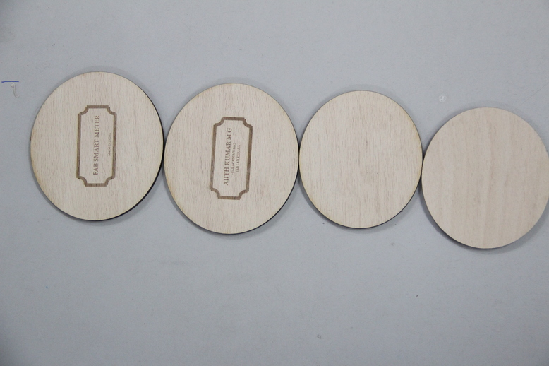
The below showed image is the changed name plate from Fab Smart meter into Easy Tester
The final part is assembled using the sythetive adhessive resign, a wooden strip is also given as a support for fluxture opening. Smoother fabric material is cut into the required shape and pasted it using the resign. A welvet kind of packing sponge was there with me i used it on the opening of the bos to avoid the scarches on the LCD.
Download carry case box production files(.zip)
Total skills i used in making the Esy tester is shown below
Licensing Easy Tester project
I am Licensing this work under Creative commons -Atrribution (BY)- NonCommercial (NC)- SahreAlikie (SA)

This work is licensed under
	 a Creative Commons Attribution-NonCommercial-ShareAlike 4.0 International License..

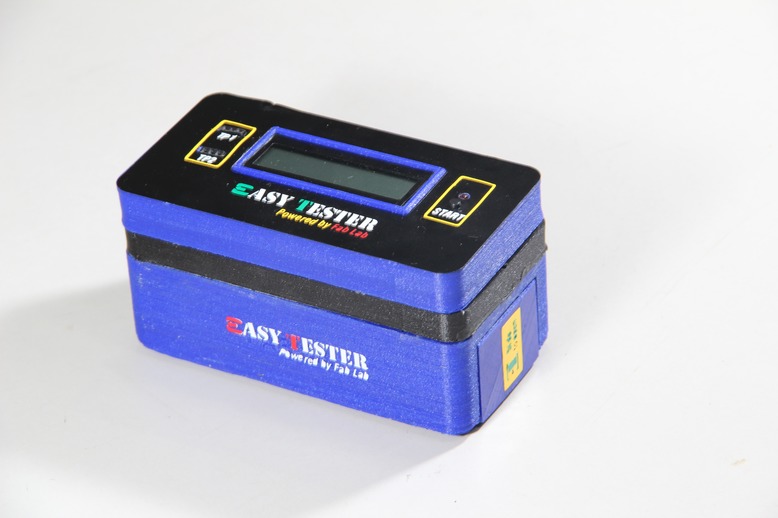
Hero shot of my Easy Tester Powered by Fab Lab is shown below.
Working video of Easy tester is shown below
Download center of Easy Tester
Quote of the Week
"Live as if you were to die tomorrow. Learn as if you were to live forever"
by Mahatma Gandhi