
Output Devices
Assignment; add an output device to a microcontroller board you've designed and program it to do something
For this week I decided to start working on my Final Project, an Ad-Clock. Part of the clock will be an LED Matrix which can be used to display ads.
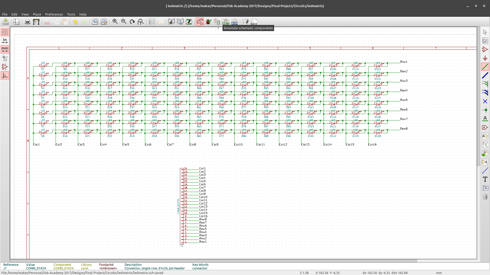
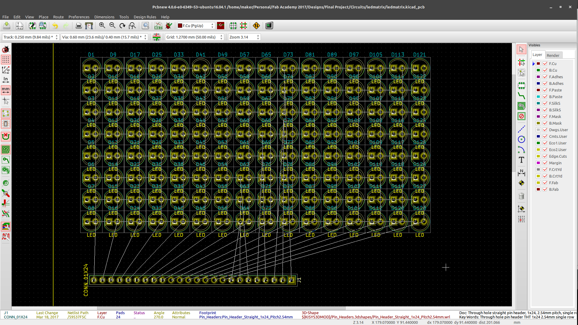
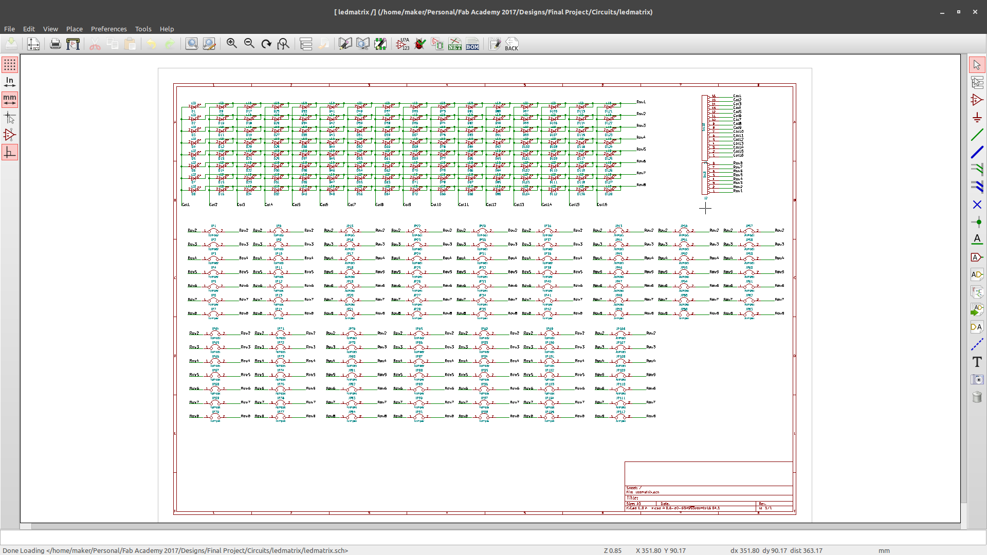
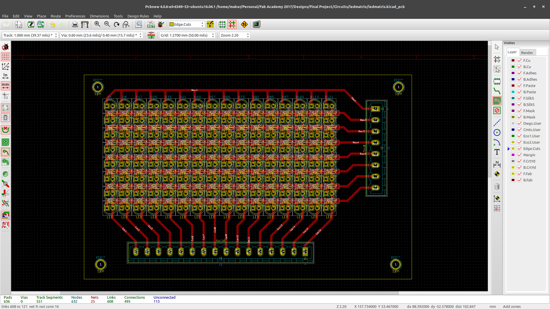
For this part I inted to use a 16*8 matrix and so I started by designing the LED matrix which proved to be the most complex part. I initially started the design in Eagle...
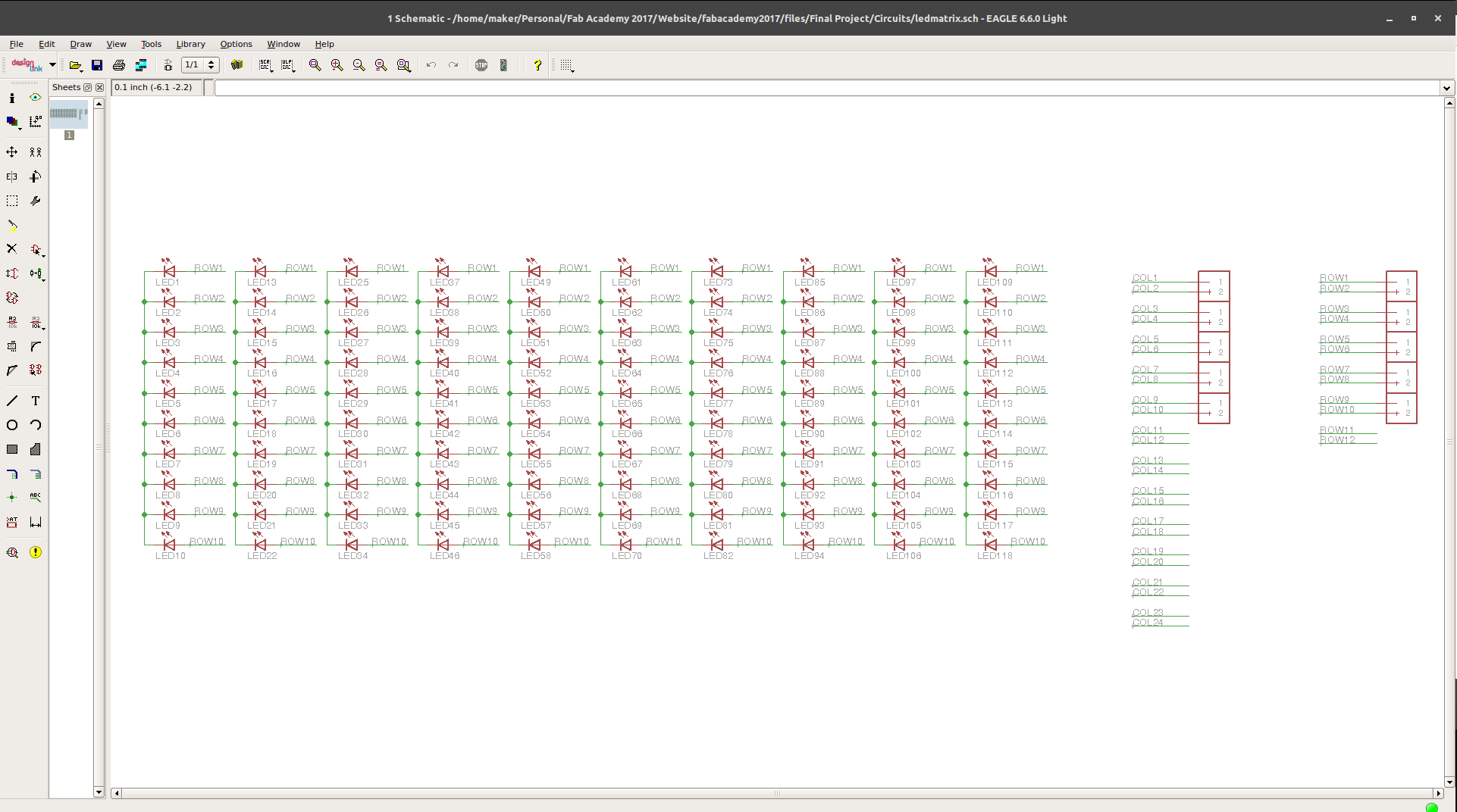
Until I hit a snag while routing my board...
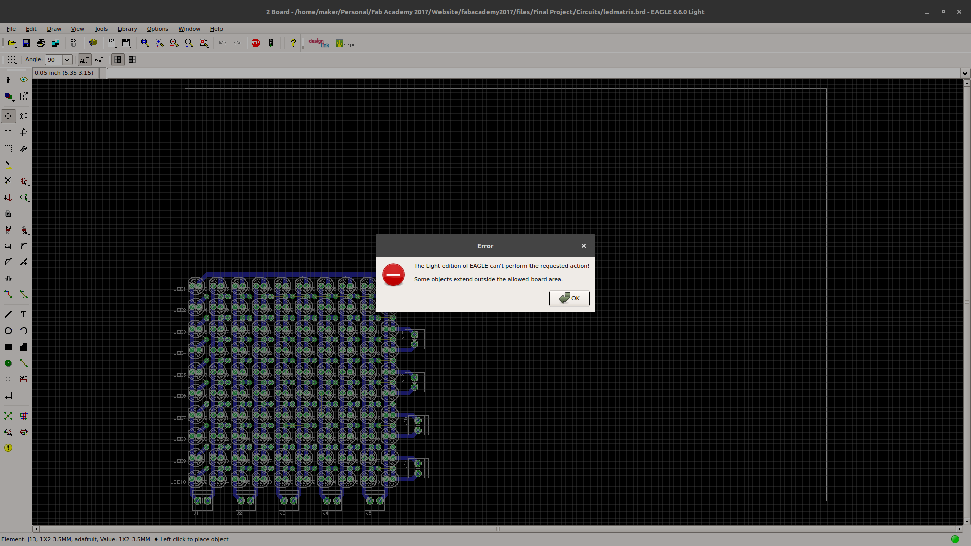
My free versionn of eagle would not allow me to exceed a specific board size and so severly limited the size of my matrix.
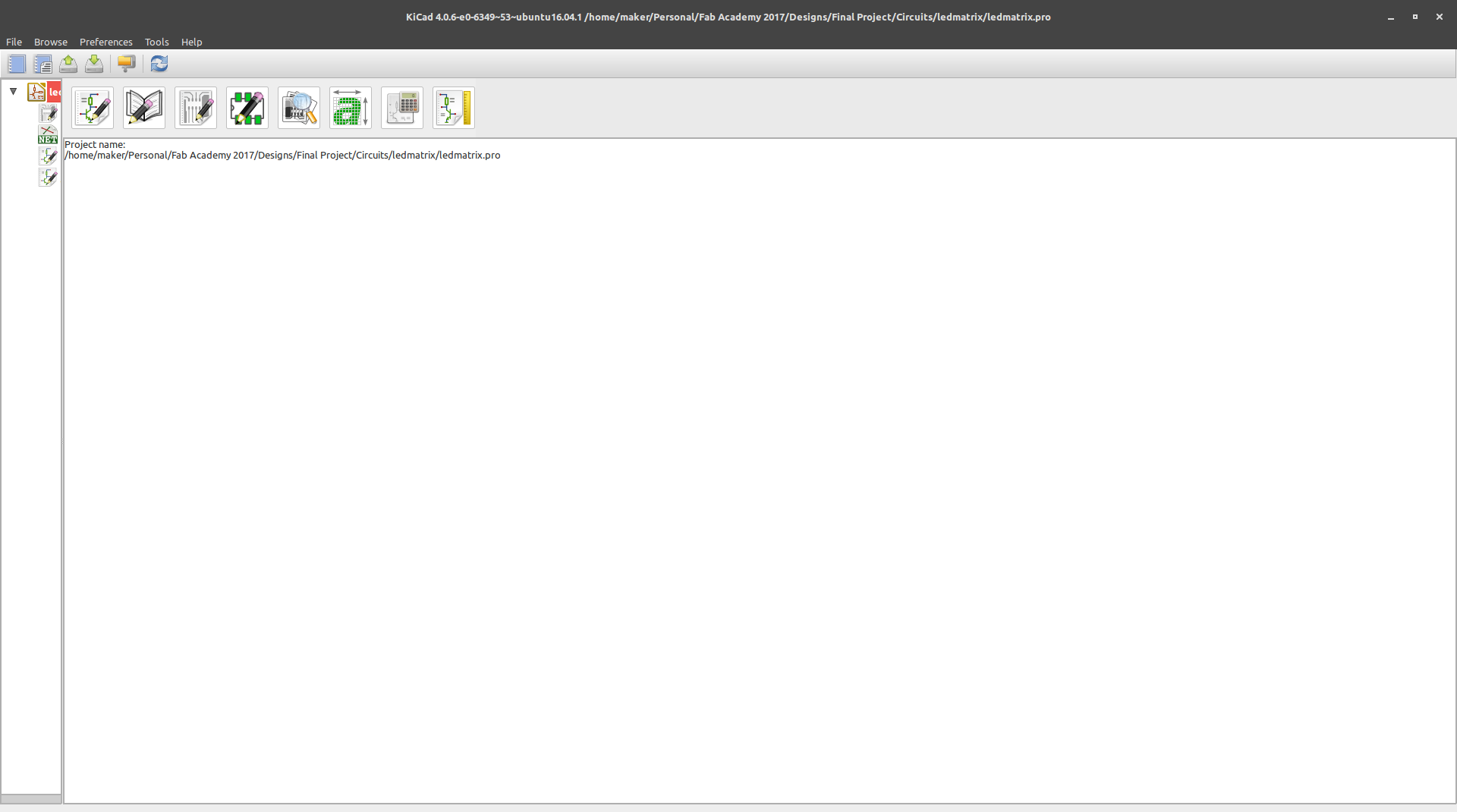
I thus took the opportunity to learn and use other Schematic and PCB editing sofware. The choice for me was between gEDA and KiCad.
I chose KiCad which incorporates the following tools...
- KiCad - Project manager
- Eeschema - Schematic editor
- CvPcb - Footprint selector
- Pcbnew - Circuit board editor
- GerbView - Gerber viewer
- Bitmap2Component - Converts bitmap images to components and/or footprints
- PCB Calculator - Calculator for components, track width, electrical spacing, color codes, and more…
- Pl Editor - Page layout editor
I launched KiCad and opened a new project,...
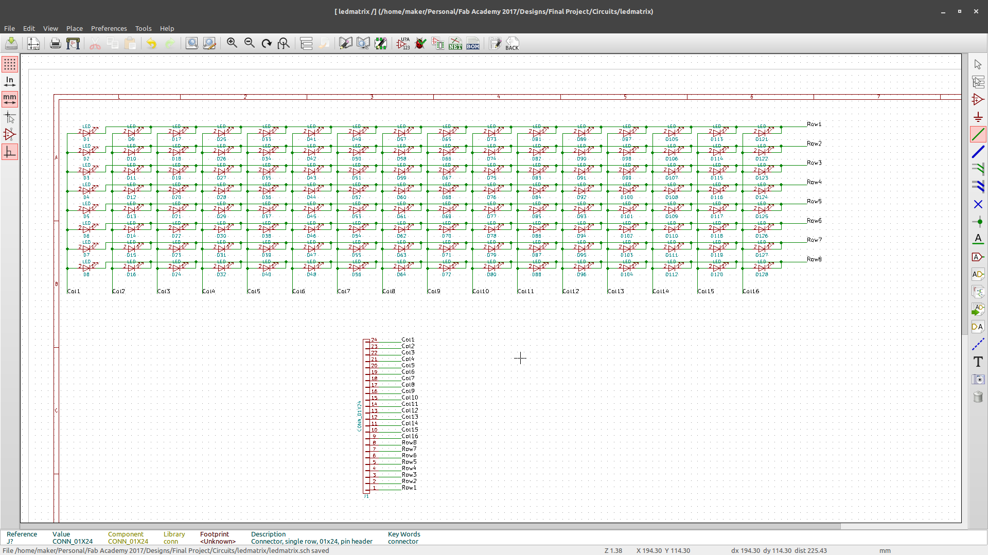
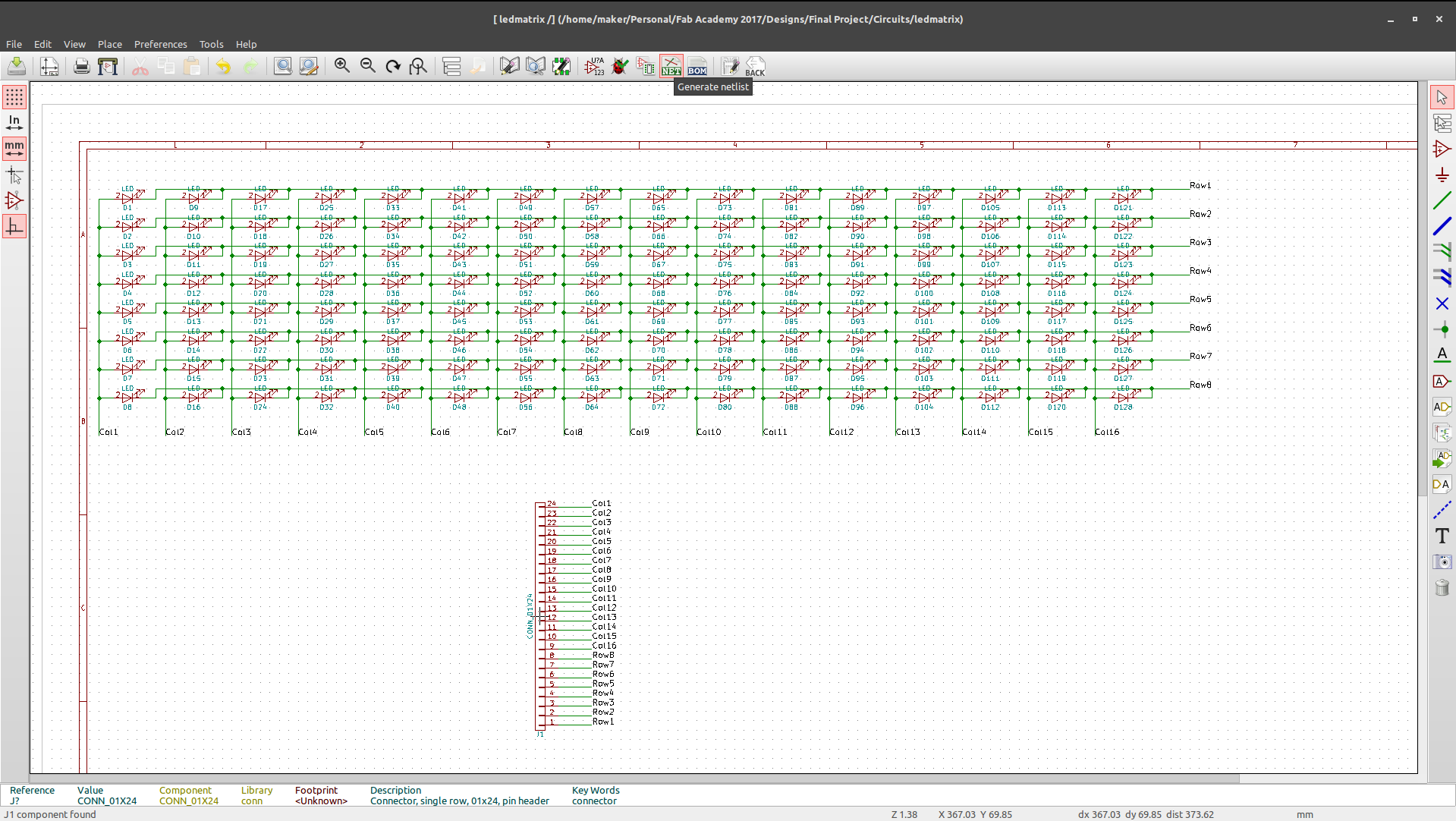
Opening a Schematic and placing components...
In order to create a pcb, I followed the following procedure;
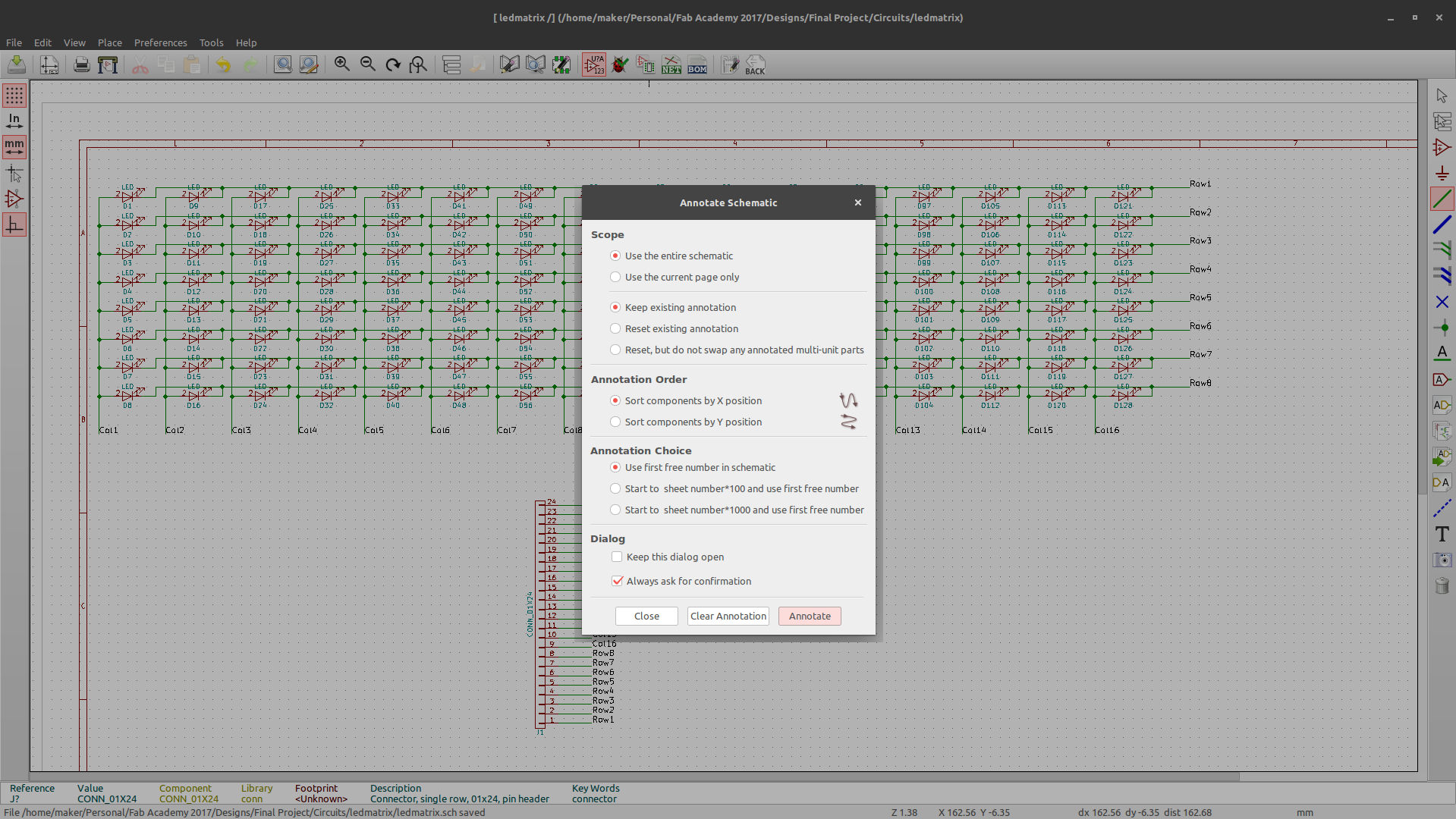
First annotate the schematic...
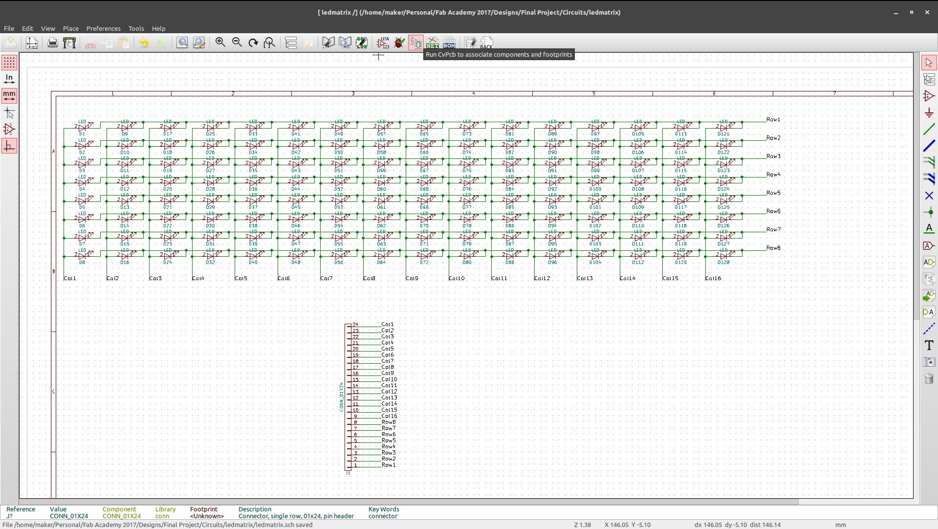
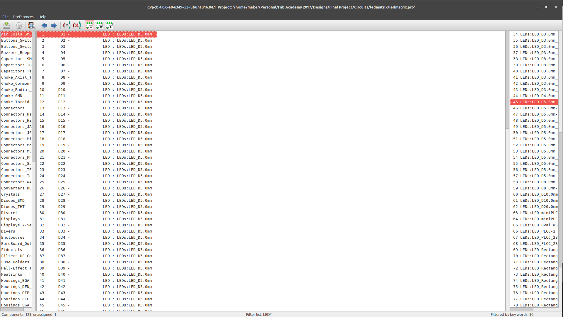
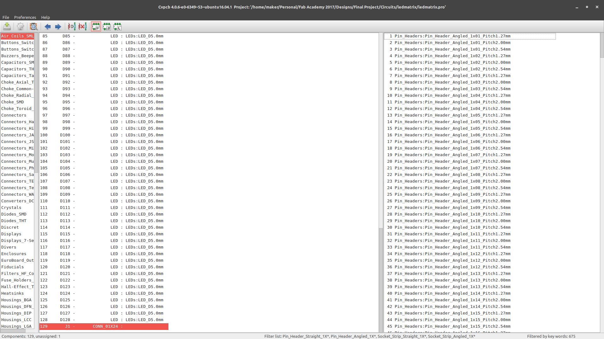
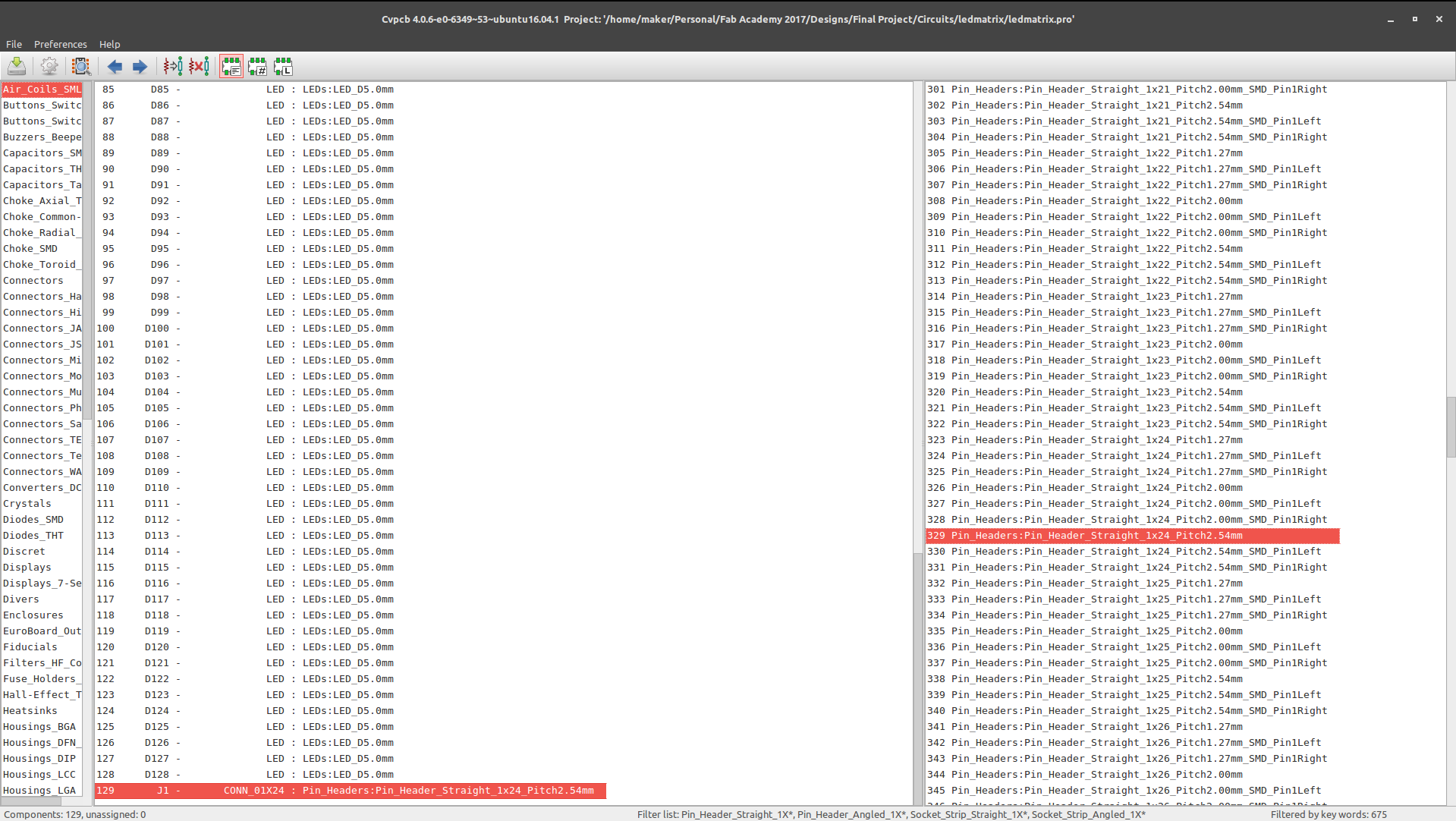
Once that is done, associate footprints with components...
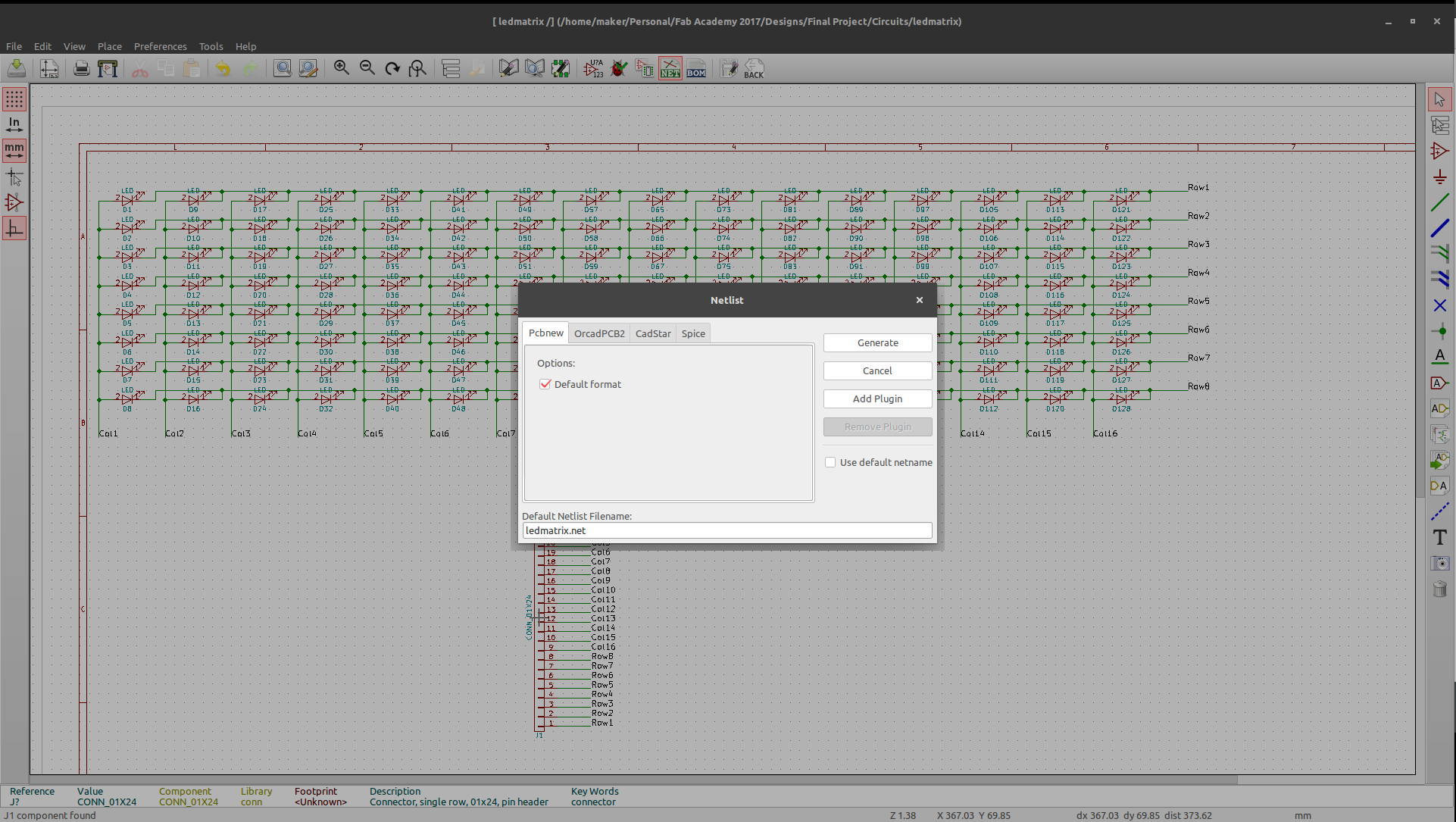
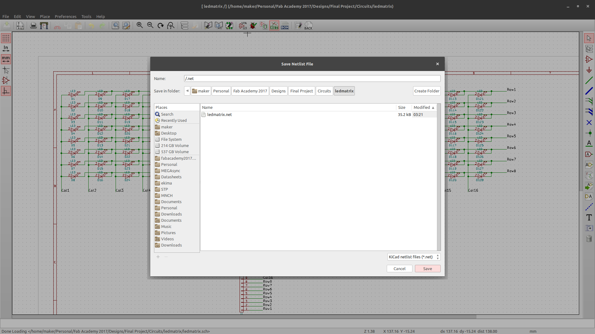
Next up, create and save netlist...
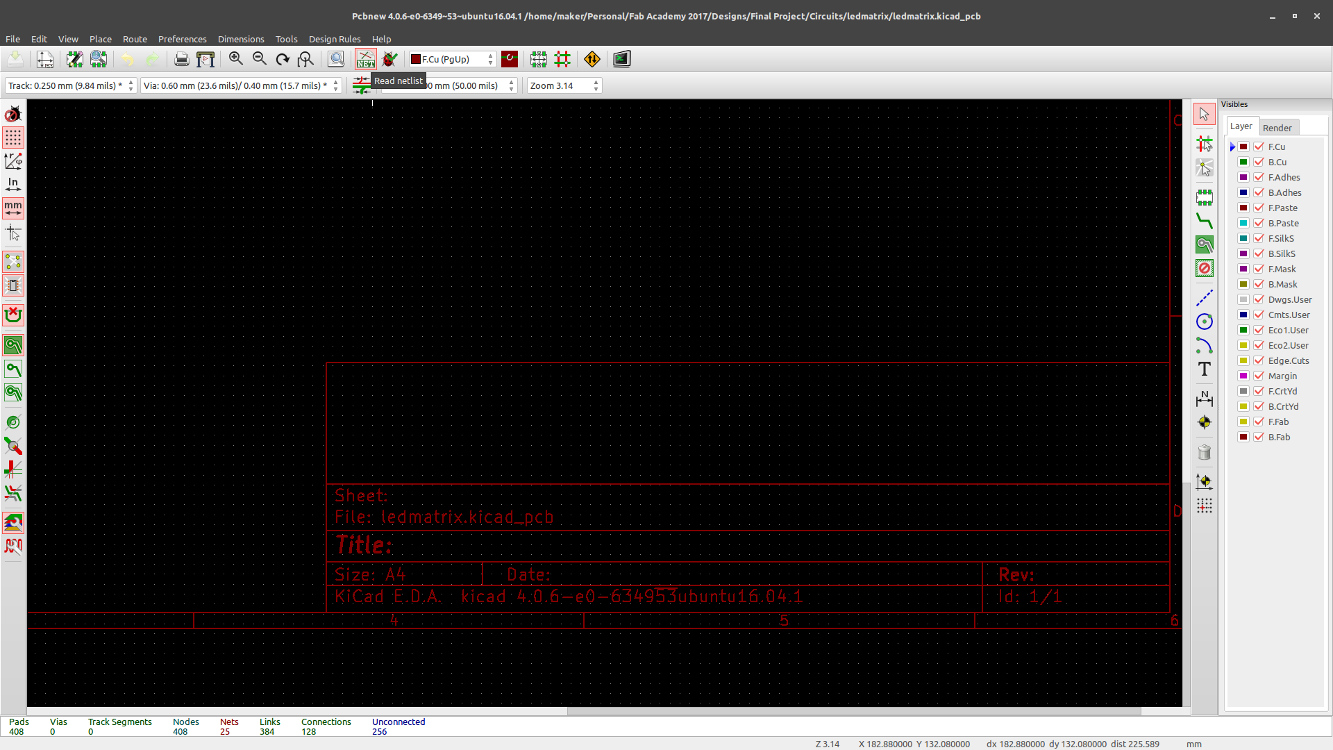
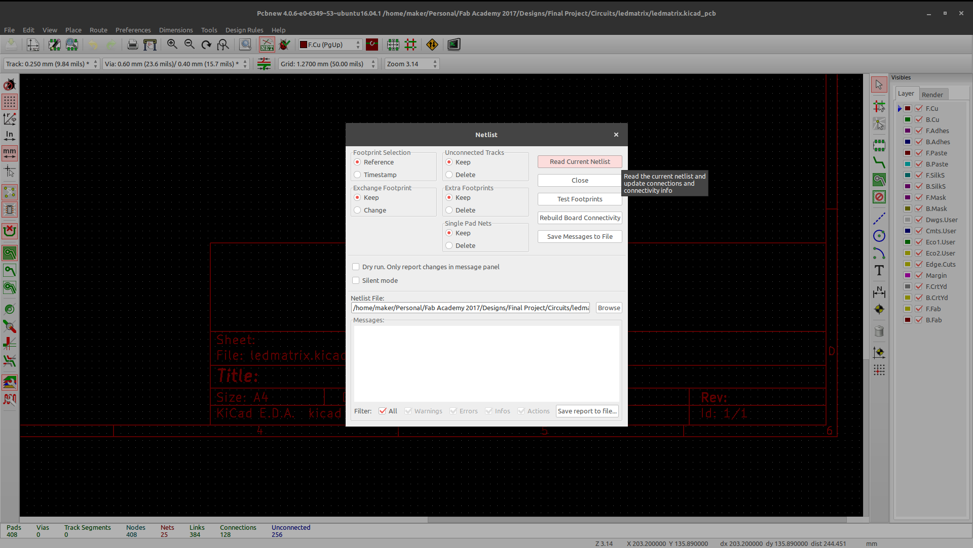
Open PCBnew and import netlist...
add an output device to a microcontroller board you've designed and program it to do something
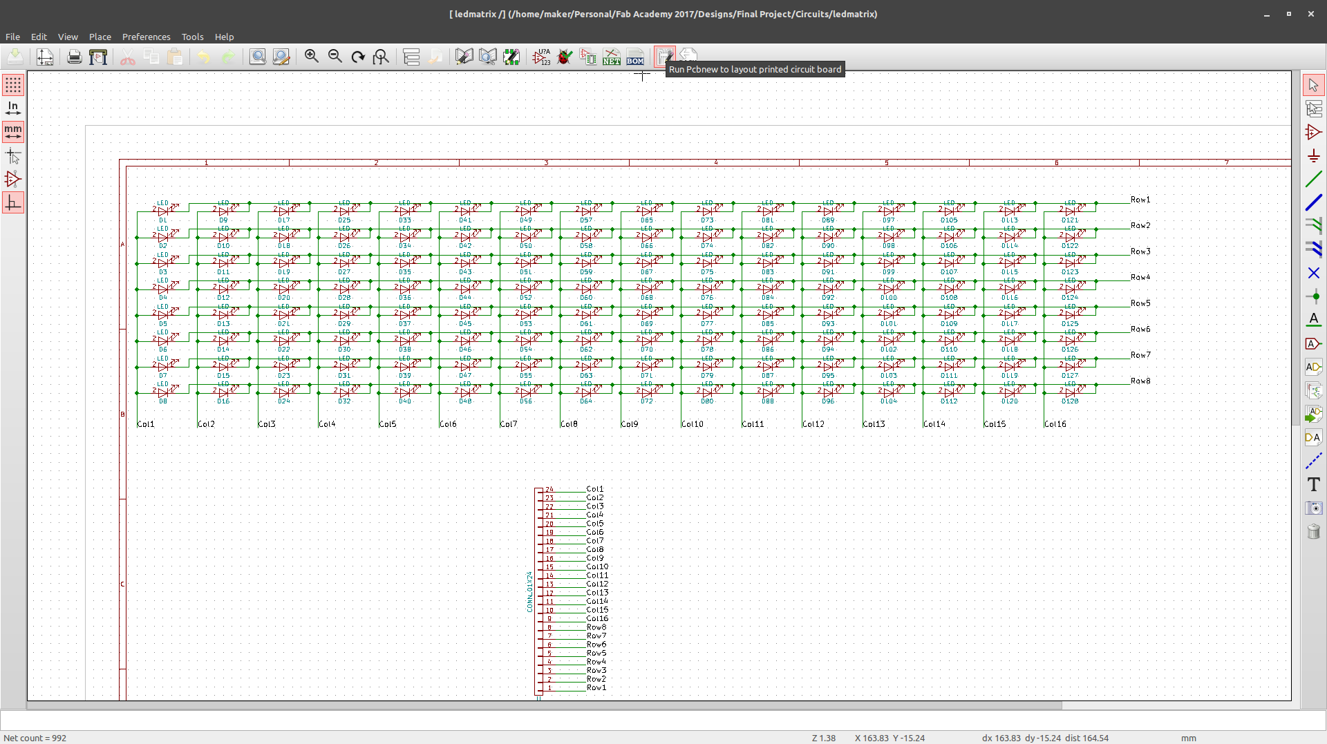
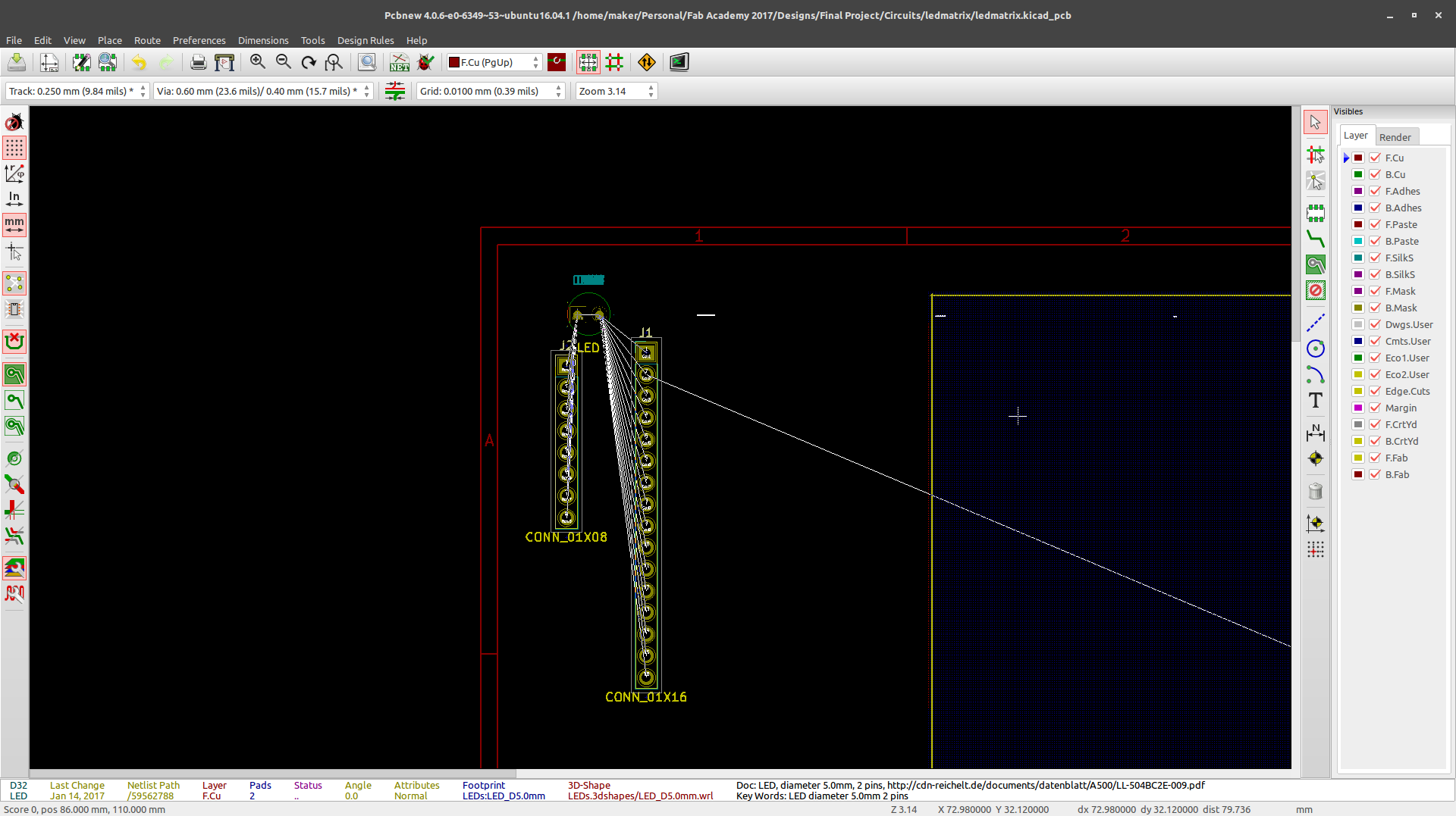
In my case,seeing as how my circuit had a lot of components (128 LEDs to be exact) I attempted to use the autoplace tool which was a complete bust...
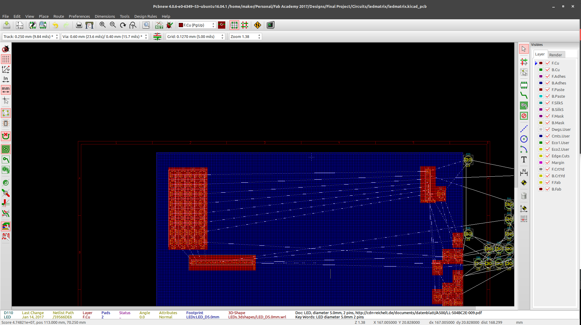
I therefore arranged all components manually...
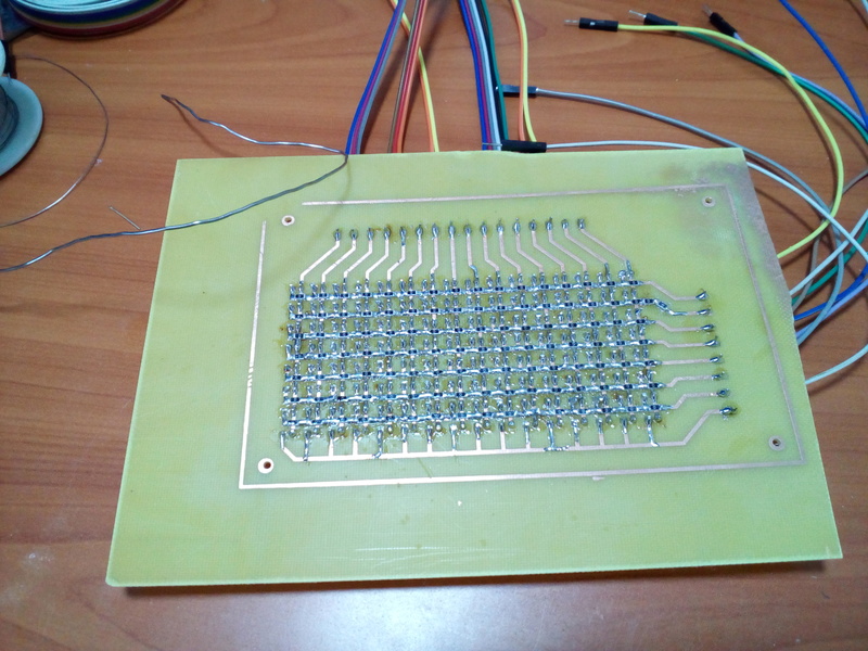
At this point I realized that routing would prove to be a problem as one set of LED Pins will have to go over the other set, i.e. either rows (cathodes) over columns (anodes) or vice versa.
To solve this issue, I introduced jumpers and set their footprint as that of 1206 SMD Resistors allowing me to use 0Ohm resistors as jumpers.
I was then able to route the board.
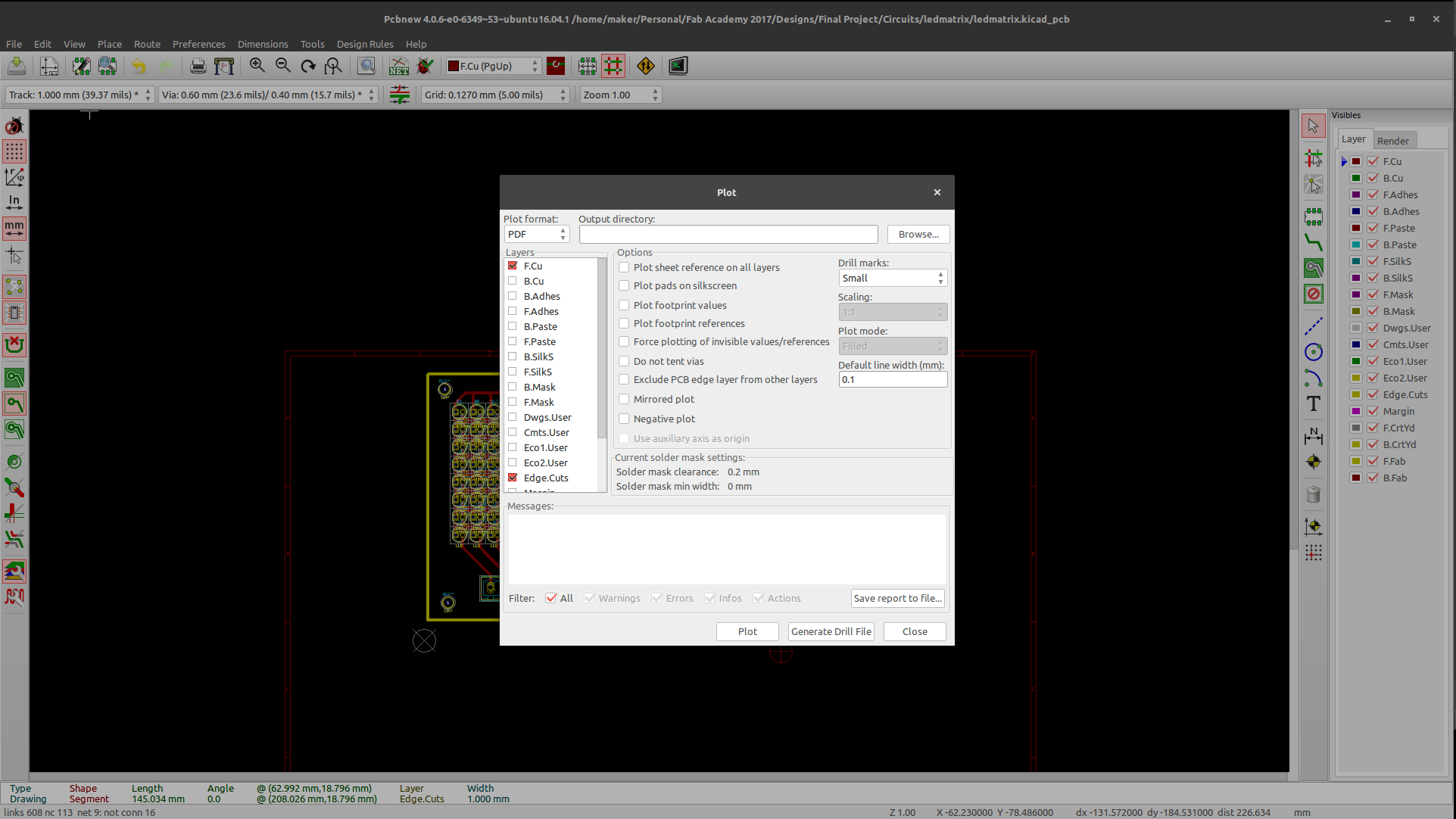
Since I was going to use toner transfer method to transfer the circuit then etch, I needed to export a pdf file for printing, so I used the 'plot' option under files to export a pdf image of the footprints and the routes.
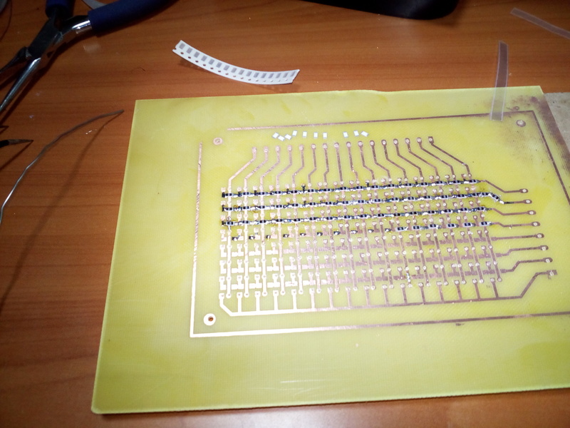
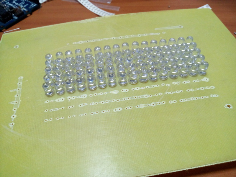
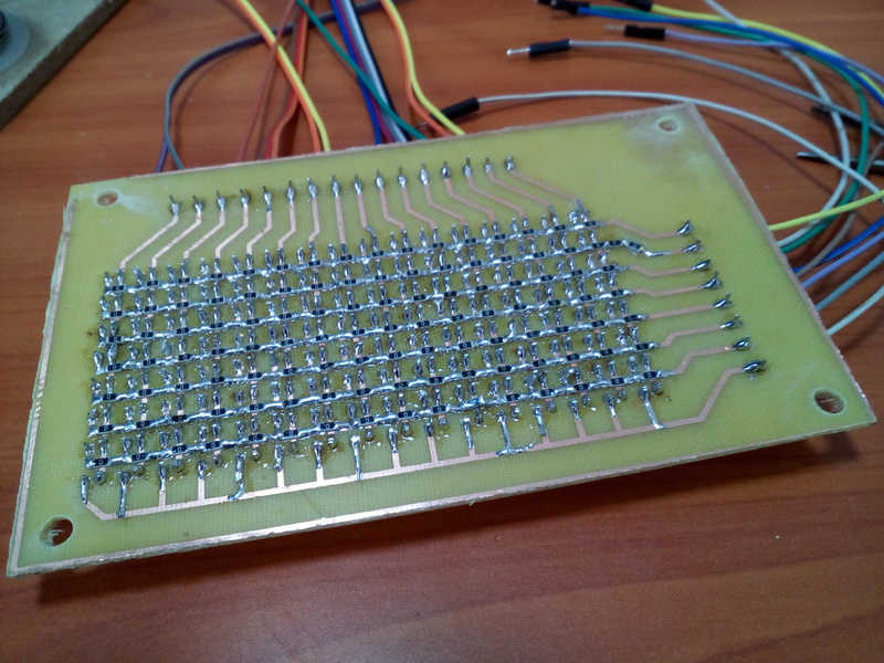
After etching, I drilled holes for the LEDs, yes all 256 of them plus 24 for the pinouts, and stuffed the board. It was quite the task and so I had to come up with a way to make it easy. Method;
Start with smd components i.e. the resistors and mount them row by row and confrim continuity of the row once you are done with it. It you wait to do this after you are done soldering all resistors you will have a hard time troubleshooting any short cicuits, and there are bound to be quite a few.
Next solder the LEds. Again do this row by row. First solder one foot for all LEDs on the row then one by one, as you melt the solder for each, confirm that the LED is flat on the board by pushing it gently. Next solder the remaining foot and confirm continuity.
Halfway through soldering the resistors...
I found a simple trick where I use my Digital MultiMeter to check connectivity. Instead of checking for continuity, I used the same setting to light the LEDs. My DMM uses ~3V to check continuity and so by placing the negative (black) probe on the row, I would run the positive (red) probe along the columns and thus light the respective LED and killing two birds with one stone; confirming that the LED works and that there is no disconnect.
Halfway through soldering the LEDS...
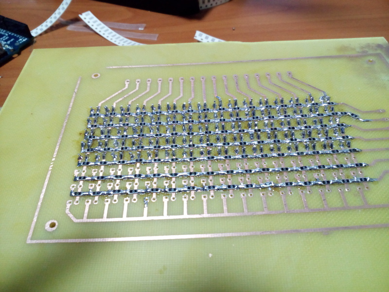
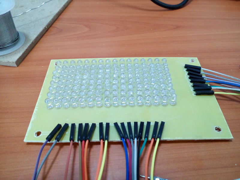
Finally done all soldering work...
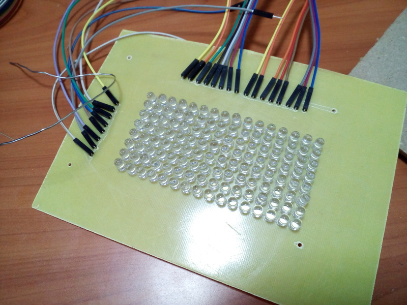
I then resized the board and drilled mounting holes.
Next up, the control board which is the 'brains' of the matrix. This I designed in Eagle.
Assignment wise:
- Add an output device to a microcontroller board you've designed and program it to do something
Files
KiCad Files.