

Week 4 - Electronics Production
![]()
![]()
Assignment
make an in-circuit programmer by milling the FabISP, then optionally trying other processes.
![]()
0. Preparation:
This week we have to build up our own FabISP programmer. I have to learn to use the LPKF milling machine, solder the components to the board and load the firmware on the chip.
The FabISP is an in-system programmer for AVR microcontrollers designed for production in a FabLab. It allows you to program the microcontrollers on other boards.
![]()
For designing and layouting pcb-boards you need to Download Eagle from Autodesk
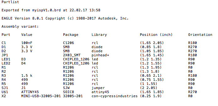
Partlist exportet from Eagle:
![]()
Florian, Aleks and me needed additional pin headers to connect the external programmer to the AtTiny. The website of Dr Azzy was a good help to insert the missing smd pins into our eagle library
![]()
According to our instructors Tobias, we were based on the work of Brian's programmers, based on Zaercs programmers from FabAcademy 2015.
![]()
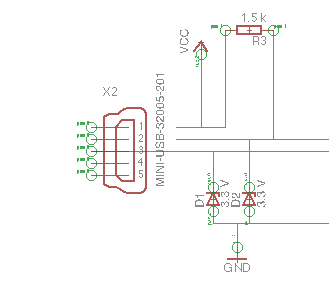
- Change: USB-AB port instead of USB drive as connection
![]()
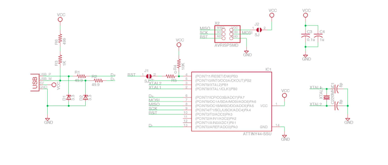
1. Schematics:
![]()
As I already mentioned in the global review with Neil, I am a primal mechanic and have absolutely no knowledge of electronics production and design.
![]()
After some failures and some perseverance, a skype conference with my instructor Tobias helped me, to design the right approach and the correct schematics:

![]()
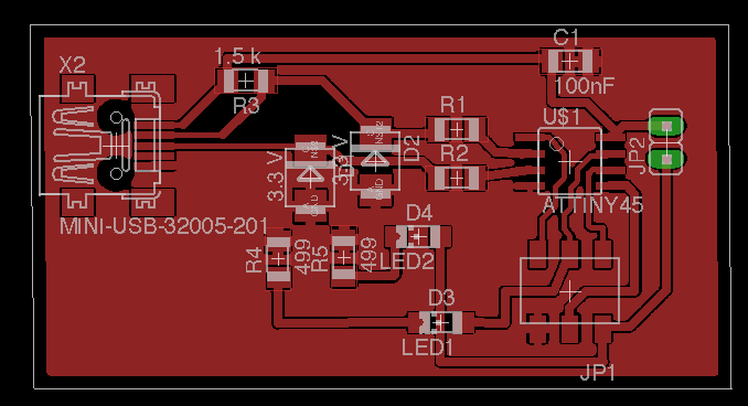
2. Board layout:
![]()
At next, the layout of the board must be created. All routes must be set to connect the parts. To switch to the board layout view, change to the board view at the top of the toolbar.
Now it is important that you arrange all the components in a poligon sequentially prepared in the field:

My instructor Tobias told me about the rastnest function. (A function in the circuit board layout, with the possibility to connect a signal to the entire copper area, which is located between all parts on the board).
It is a really good technique to use the GND signal Over the entire layout, set the 'name' of the rect to GND, and press the rastnest button
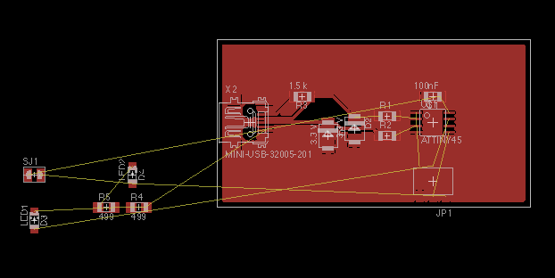

On the following picture is the final version of my own designed pcb-design:
3. Milling and prepare the pcb:
LPKF ProtoMat S63 and LPKF ProtoPlace S
In the next steps of this documentation I will go into the production and assembly of the pcb:

- The LPKF ProtoMat-S series is suitable for almost all applications of in-house prototyping. The ProtoMat S63 is able to handle the 2.5-dimensional material processing and has an increased spindle speed of 60,000 rpm. It is therefore also suitable for drilling test adapters and for housing processing.
The systems are supplied with software that develops workflows optimized from current CAD data. All ProtoMat series plotters can be upgraded step by step to the full range.
- The LPKF ProtoPlace S is a semi-automatic pick and place system for the professional SMD assembly of PCB prototypes and miniature labs. With it, SMT circuit boards can be equipped much faster than before.
The LPKF ProtoPlace S supports the precise SMD assembly of high-frequency circuits. A camera system with color display makes it possible to conveniently control the positioning.
Source: www.lpkf.de
In the regional review with our instructor Tobias and our FabLab Guru Daniele I was pointed out that this assignment is missing an explanation of the LPKF software. So I have written a short tutorial for using the software:
Curcuit Pro Tutorial for single sided pcbs
The circuit pro software comes with the lpkf milling machine. To mill the eagle-designed boards you have to use this software.
2. Start the Autodesk Eagle software and open your design. Go to CAM/Job/Export LPKF-file.
3. Select Process Job.
4. Start the software „Circuit Pro“, and choose
File/Templates -> Single Sided Top sector.
5. Choose Process Planning Assistent and select Edit Circuit Board:
Set to:
5.2 Material: FR4/FR5.
5.3 Then click: ready.
After setting it click Open. The board now loads into the software.
7. Select: Cutting Generator and select: Isolation Method.
Single, Pads double and the milling depth:
In my case 18µm. After you have done this, you can close the window.
8. Choose: Circuit Board Fabrication Assistant.
If all settings have been made correctly you can press Start.
9. Choose: Material Setting and check the settings. After that press Proceed.
10. Select: Positioning by Mouse Control. Now select an area on which the layout is to be milled.
Deselect the Mouse Positioning and drag the Layout to this position.
It is very important to deselect the Mouse Positioning after that.
Now you can Save the CAM-job as .cbf-file.
After saving the .cbf-file the LPKF starts to warming up the milling spindle and start to mill the pcb.
I have also found a very good video tutorial on youtube. Watch this in addition to my own written tutorial and you will understand the LPKF curcuit pro software as fast as possible: Video Tutorial
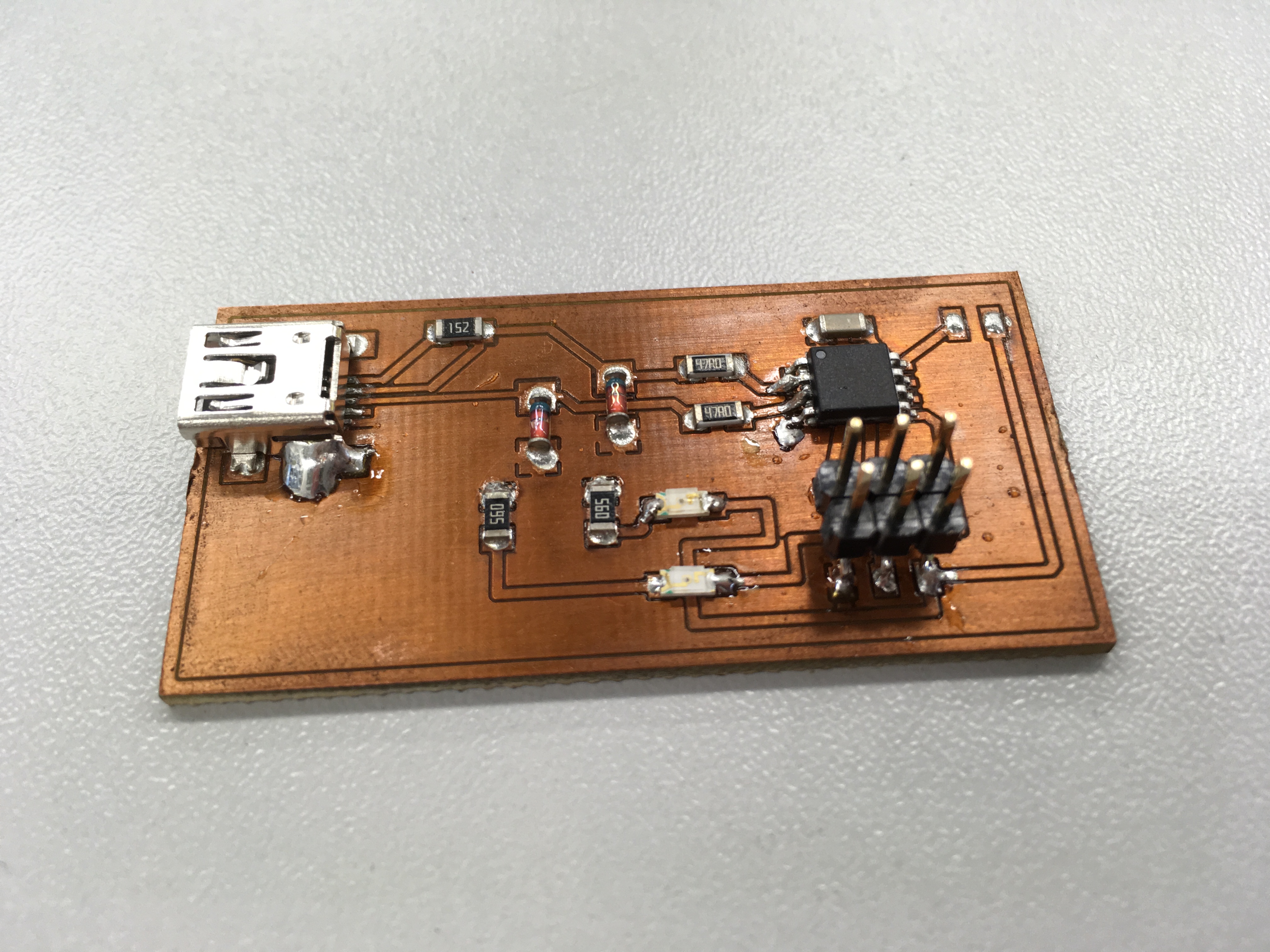
4. Equip the pcb:

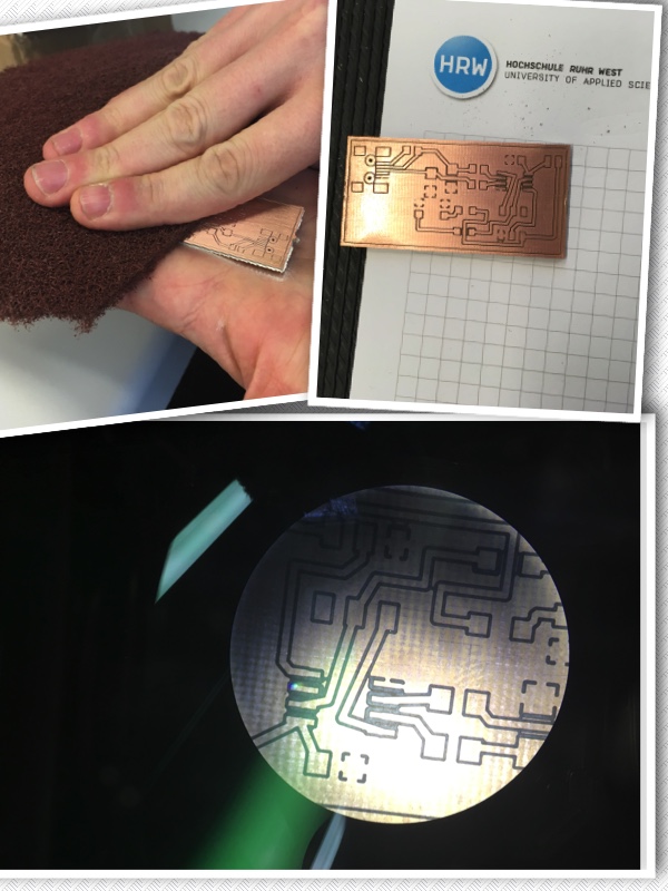
- On these photos you can see that I have a pcb polishing mat, the surface has polished beautifully polished. The surface is sprayed with a soldering lacquer at the end. For soldering lacquer I used This stuff

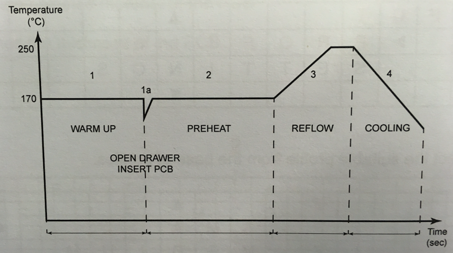
6. Bake the pcb:
The finished stocked pcb gets into the reflow-ofen done
7. Solder the LEDs and the Jumper:
- In the end I soldered the leds and the jumper by hand.
As a help: the green point on the leds is the cathode.
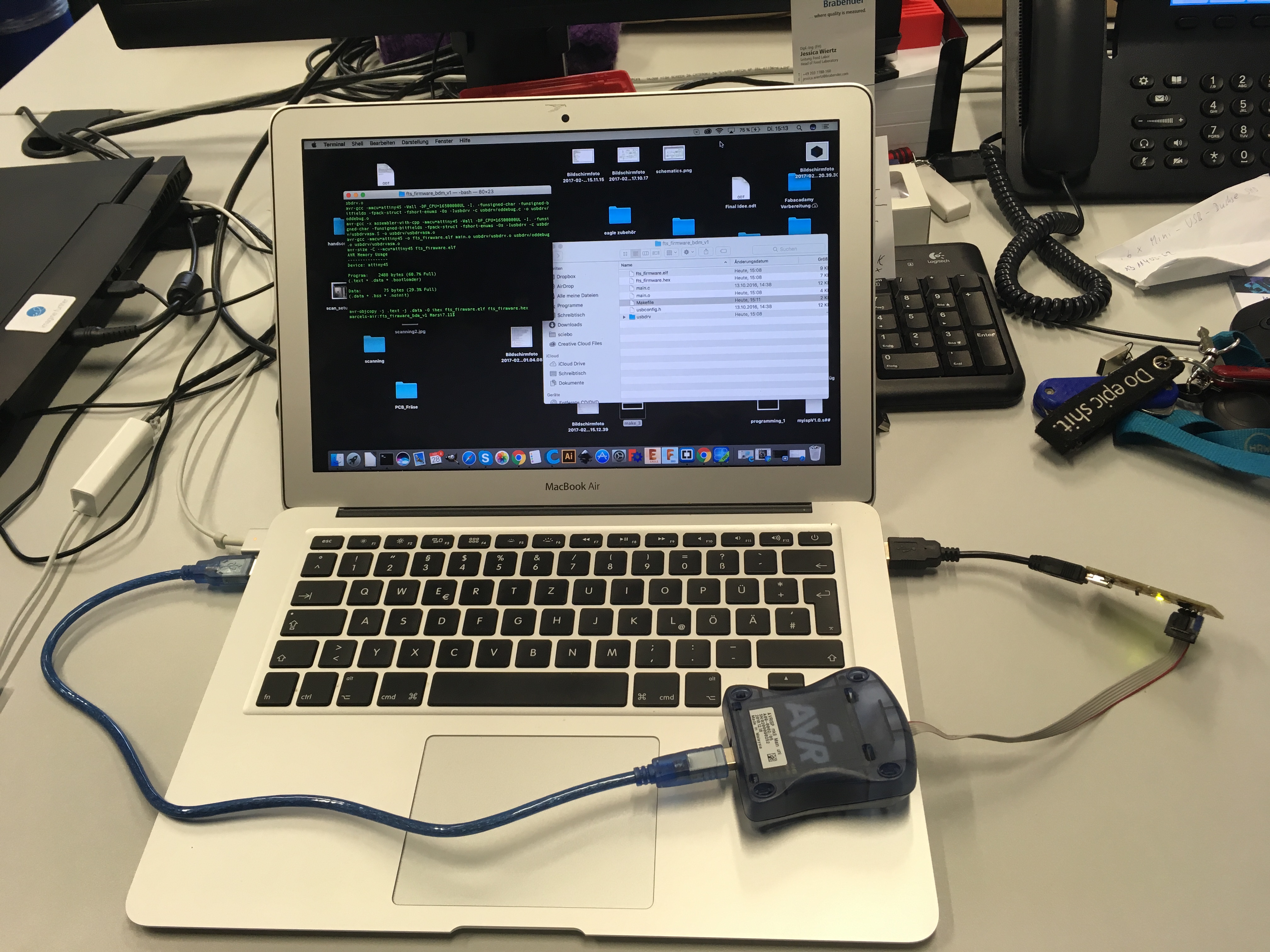
8. Programming:
- PROGRAMMER ?= avrisp2
- Learned more about electronics.
- Practiced soldering skills with SMD components with LPKF pick and place and by hand.
- Learned to use AVR-programmer to program the FABISP.
On the based work of Brian's programmers,
based on Zaercs programmers from FabAcademy 2015. Thank you for that !
1. At first i have downlaoded the crosspack from www.obdev.at

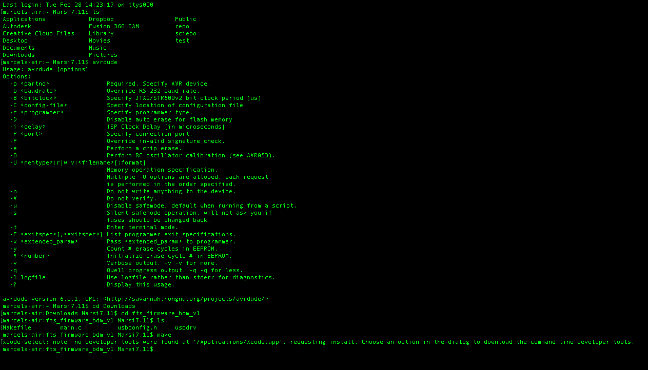
Connect the chip to the ARV programmer for preparing to flash the chip. First edit the Makefile. In the Makefile search fot the line for the programmer:
Type Programmer ?= avrisp2. This is the programmer from AVR from the previous image. There are several possible programmers but this box was what we have in the FabLab. You can find and order the AVRISP here.
The change of the line for the programmer is the only thing one has to do. Next step is to set the fuses on the chip. This can be done by entering "make fuses".
2. Edit make file to atTiny45:
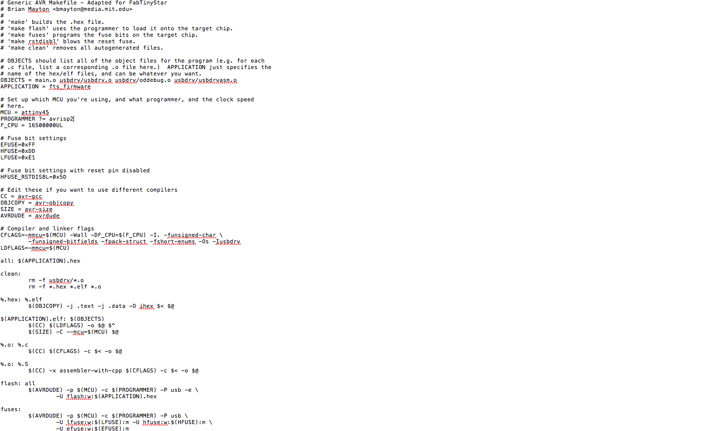
3. Make Fuses, programm, avrdude, rstdisbl:
After setting the fuses of the AtTiny I flashed the program on the ic. You start the flash progress with typing "make flash" in the console.


- Lastly I checked with my macbook air whether
the Fabisp as usb device is recognized:

Lesson learned:
Download-Section:
My FabISP-design .BRD
My FabISP-design .SCH
![]() FabISP Makefile
FabISP Makefile
FabISP main.c
eagle partlist
![]()
![]()
![]()
![]()
![]()
![]()