
WEEK 6 – ELECTRONIC DESIGN
Weekly assignment
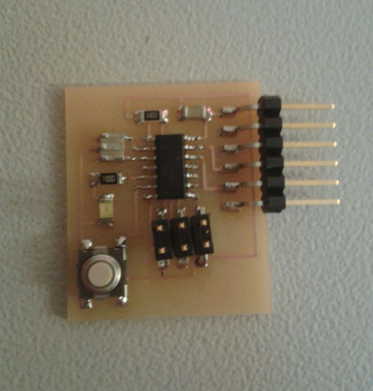
This week's assignment was to redraw the echo hello-world board, add (at least) a button and LED (with current-limiting resistor), check the design rules, and make it.
To do it I've used:
Eagle to design the circuit board
Gimp to elaborate images and to create different files for traces and outline
Fab Modules to create a file wich I could use to mill the board
I made the hello.FTDI.44 and as first thing I made a list of all components I needed.
BOM (one for each):
20MHz resonator
1uF capacitor
10K resistor
6-pin ISP header
ATtiny44 microcontroller
100 ohm resistor
FTDI header
Additional components
As I said part of this assignment was to add two components to the echo hello-world board.
Button
To know how to place correctly the button over my board I first checked the datasheet to collect information about the device.
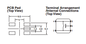
What I've found is that the pins are connected in pairs, pin 1-2 and 3-4, for this reason I had to connect one pin for each couple, to let the circuit work.
I connected pin 1 to a free ATtiny pin and pin 3 to the ground.
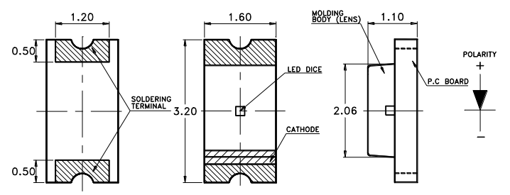
LED
Also for the LED I read the datasheet to have more information about it. Through this I've found that LEDs have a polarity wich is represented upon the component with a green line on the cathode, which is the negative pole. In this way I've known the right direction in wich place it on the board.
Eagle
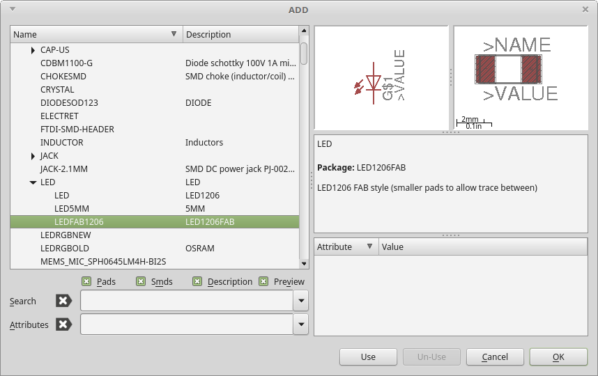
First of all I needed to download and install Eagle and to add Fab library. I've found them on the assignment's web page (here).
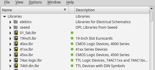
Then I had to add the Fab library to the libraries folder in Eagle. I renamed fab.lbr so I have it on the top of the list.
I've never seen a PCB design software before, and I found fundamental the quick demostration our instructor gave us. But I also needed other sources, and I've found some good tutorial on other students pages (here), on the FabAcademy tutorials page (here) and on SparkFun.
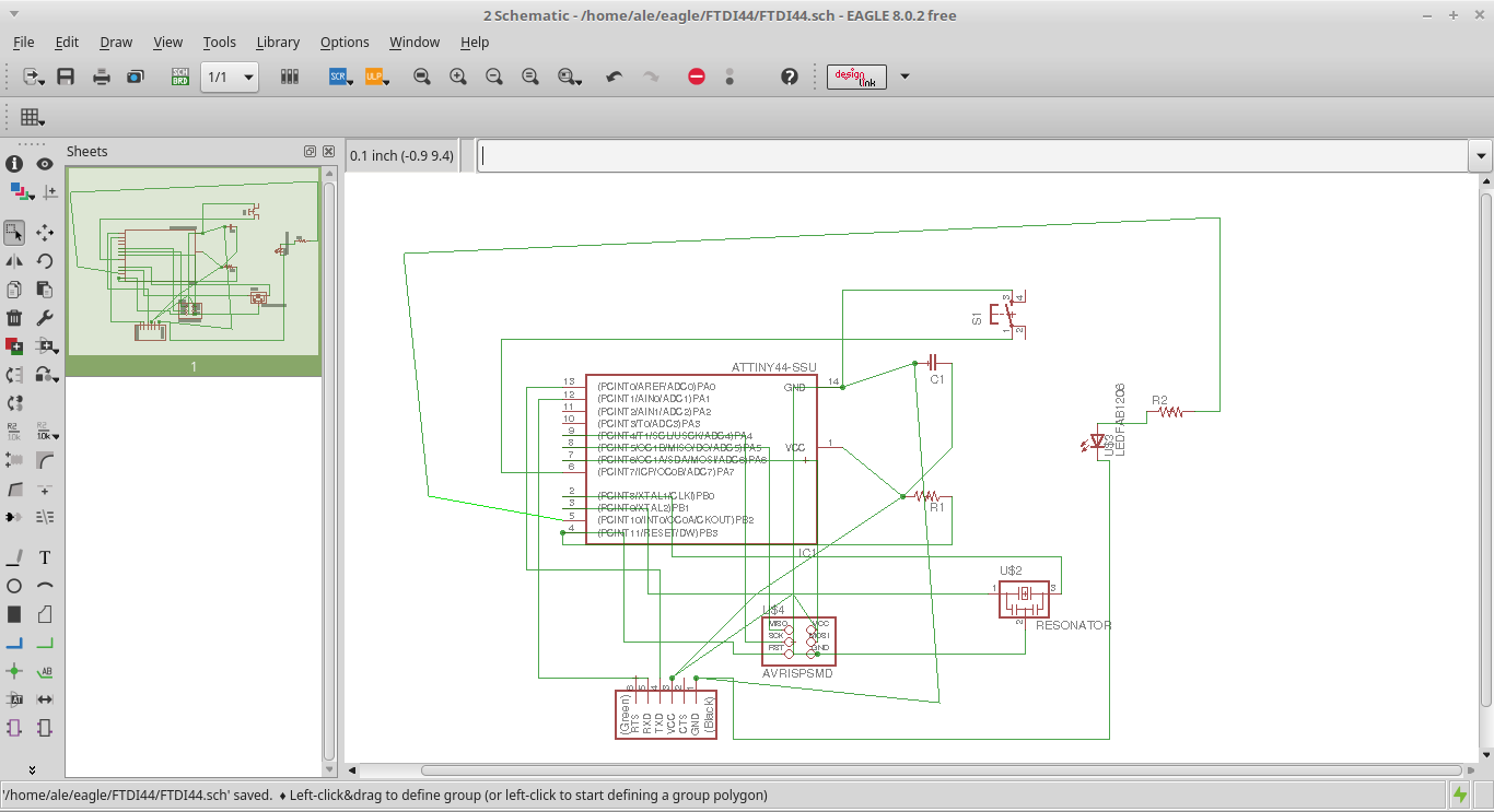
Schematic Editor
Eagle has two different editor windows for Schematich and Board Layout wich you can use simultaneously.
The schematic editor lets you make a drawing of your circuit using symbols to represent components and lines to link them each other. This is the starting point.
You simply have to select the components you need from the libraries and "add" to the drawing. I always used the Fab library and when it was possible I've chosen the fab version component.
When you have placed your component you can connect them using the "net" tool, or by the "label", it let you draw just a piece of wire and give it a name.
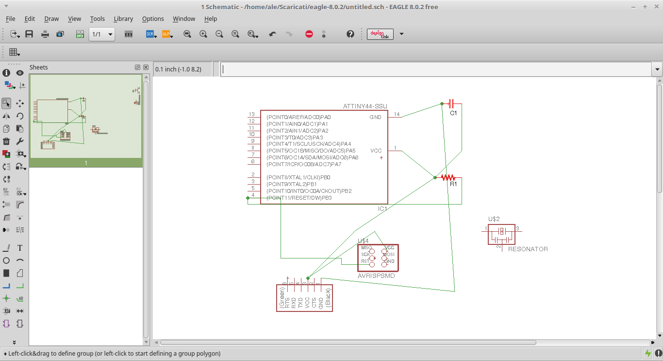
I only used "net", in fact my schematic may look chaotic.
When the drawing is finished you can check connections using the ERC tool (Electronic Rules Check)
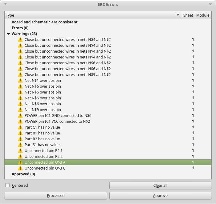
Here I recieved warnings but no errors, so I continued with the workflow.
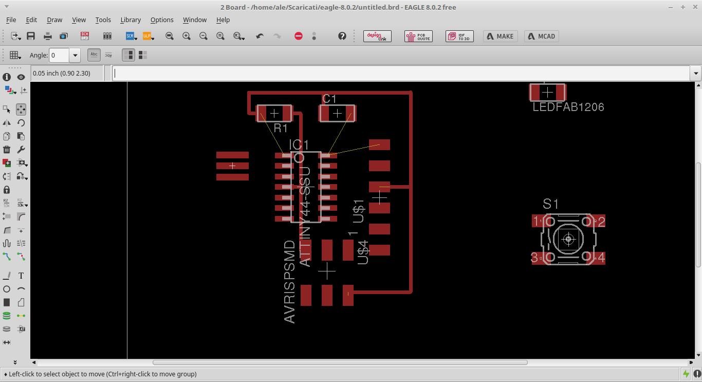
Board Layout Editor
Once the schematic has all its connections, you can move to the board layout.
Here you have a more realistic view of components and traces and their position on the board.
Using the "add" tool you can select the component and place it (moving and rotating if necessary), with the "route" tool you can design traces and break them with "ripup".
But while designing I found the movement of the pointer not fluid. To fix this I had to change grid's parameters.
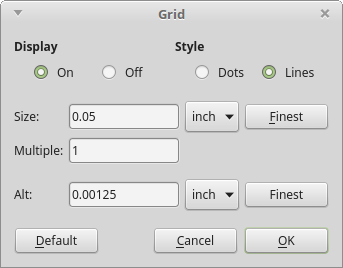
I reduced size and specially "Alt" wich let me move very precisely by keeping pressed the Alt botton on the keyboard. To lead the component exactly where wanted (with no snaps) keep pressed CTRL.
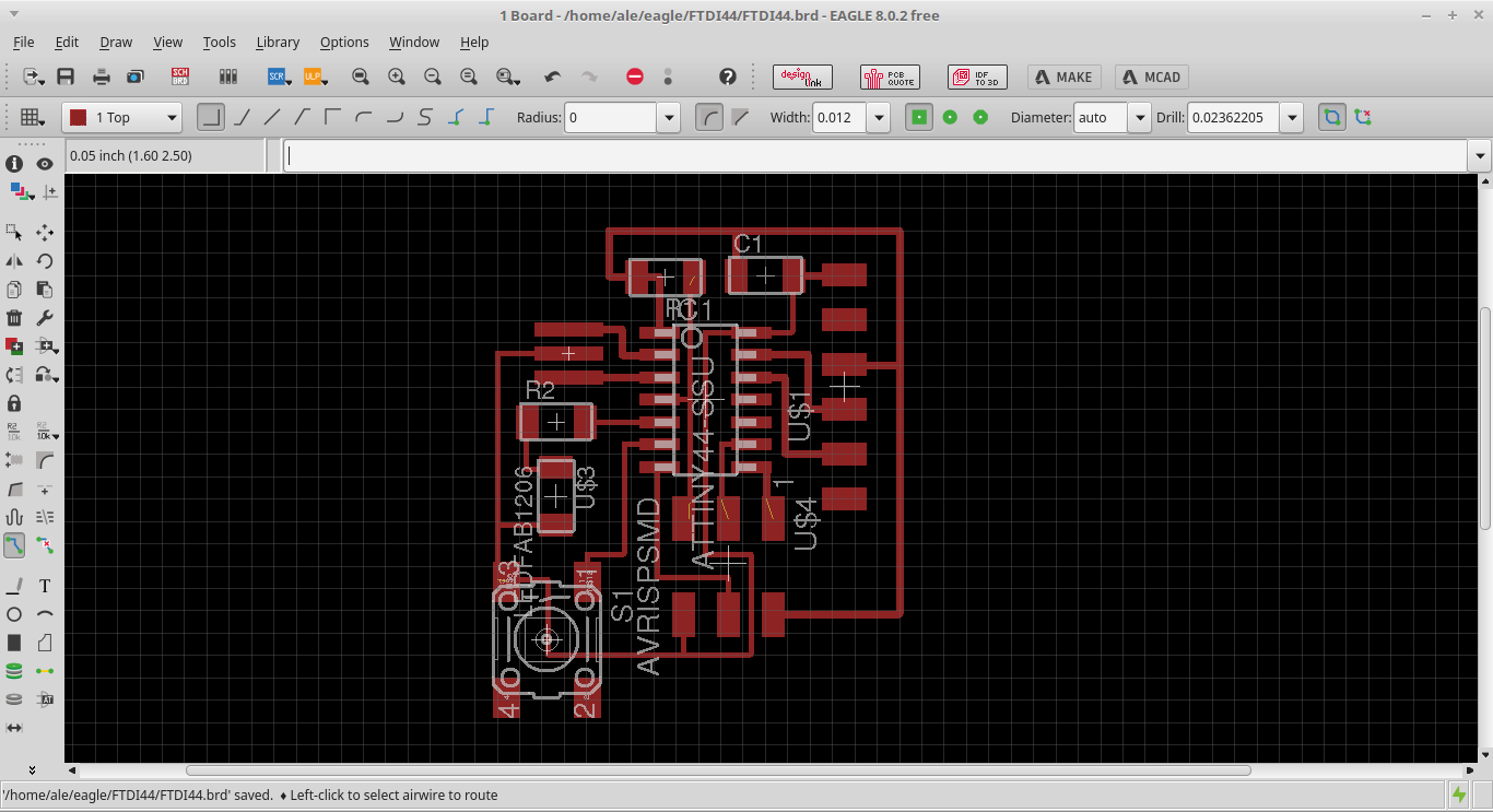
Once the board is entirely laid out you need to check the design rules using the DRC (Design Rules Check) tool.
It tells you if, according to your design settings, there is something that would waste your milling
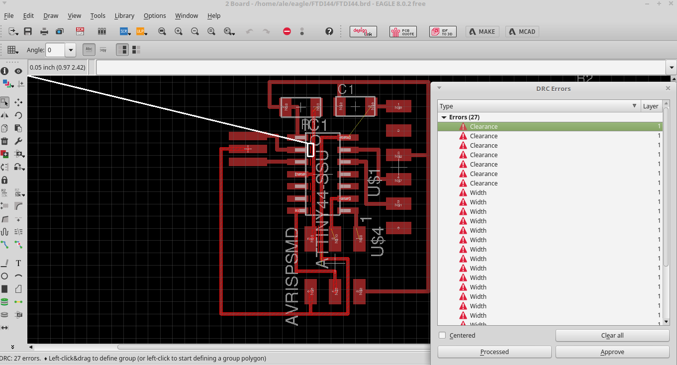
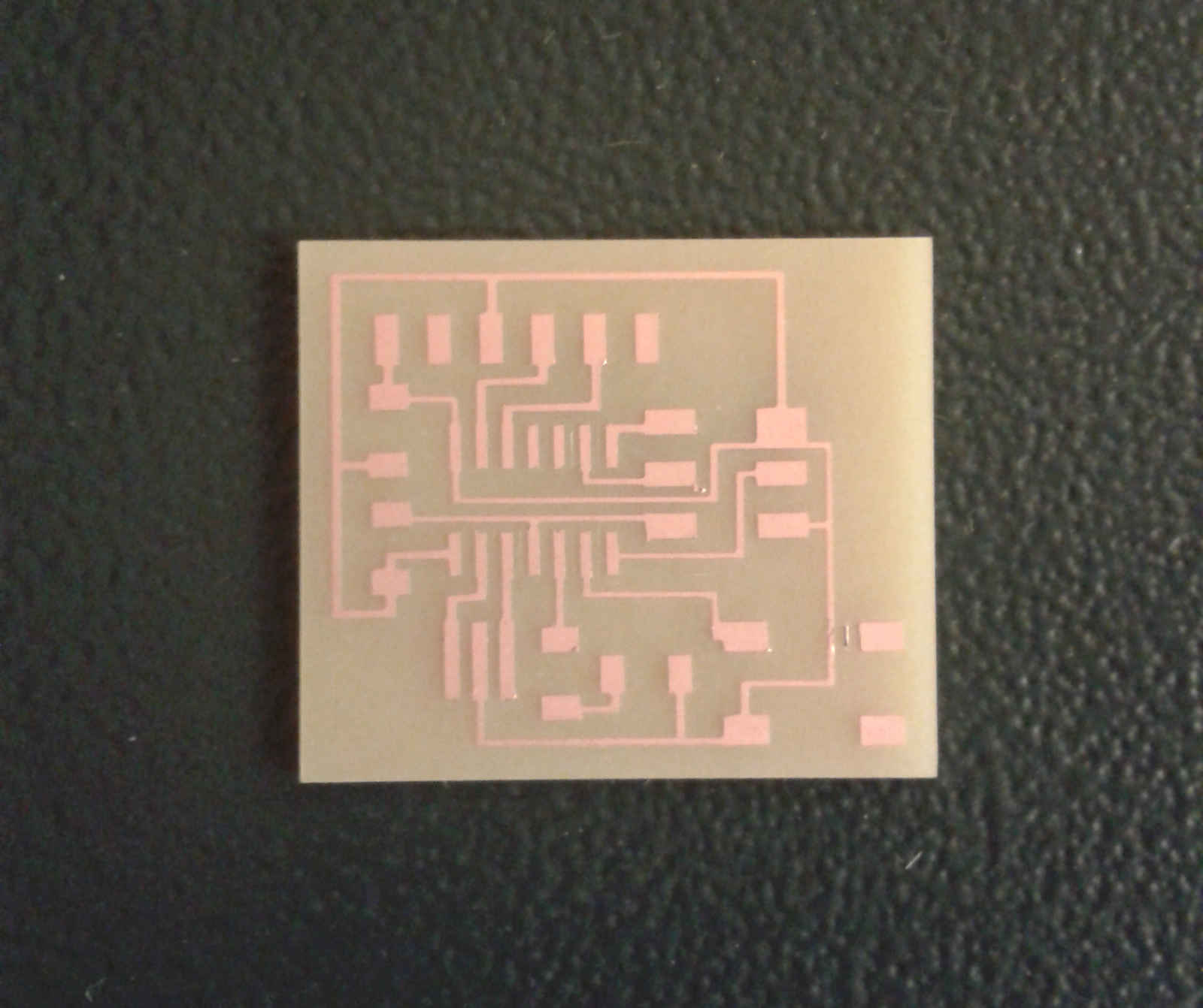
This is what I gained after my first check. The panel showed me a list of errors and by clicking on each I could see where they were. So I moved to the DCR settings, wich is shown before any check, to change some parameter.
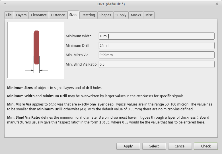
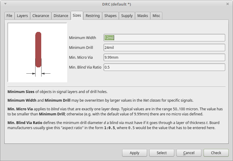
At the beginning I changed the "minimum width" from 10mill (the default setting) to 16, but to let three central traces go through a tight space I used 12mill route. So when I checked the rules I had width errors. To clear them I had to turn again the "minimum width" from 16 to 12mill. And it worked...
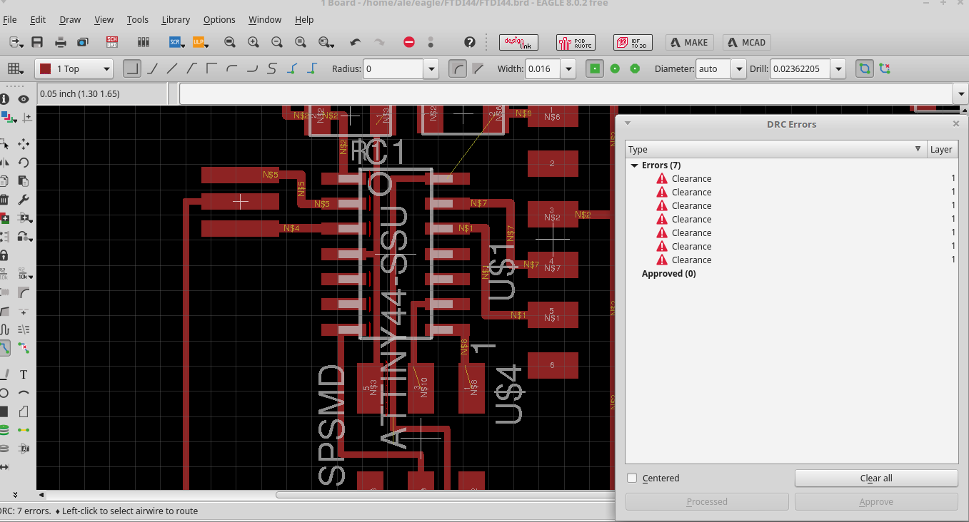
To fix the "clearence" errors (that means there isn't enough space between traces according to your settings) I just had to move the traces enough. "Clearence" is a parameter I also changed before starting, turning it from 8mill (default) to 16, because this is the minimum size for the end mills we have in our Lab.
Now I was ready to export my file...
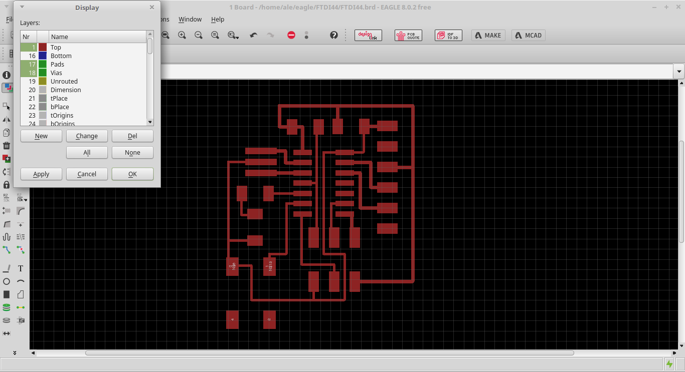
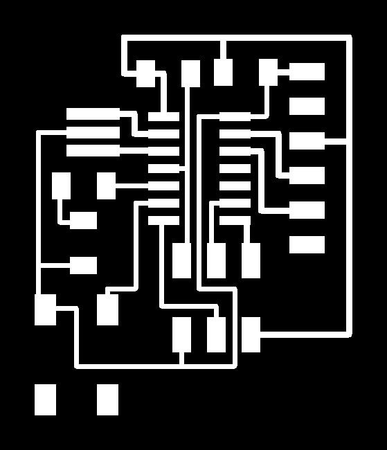
I selected only the traces layers.
Then I moved to "file-export-image" and set the resolution at 500dpi (this is the minimum size, also 1000dpi works well)
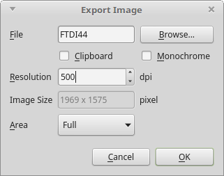
Before to save the file I've checked the "monochrome" setting to have a black and white image
Gimp
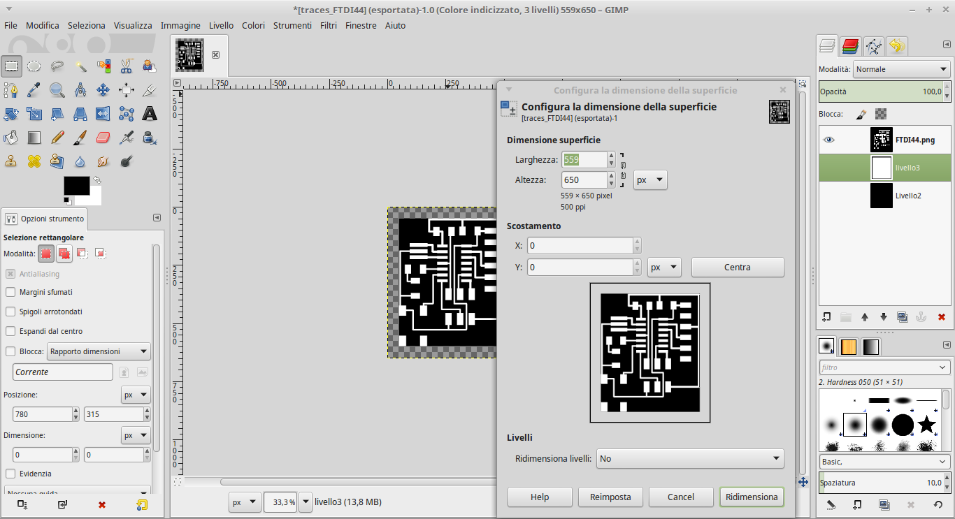
I opened my Eagle png in Gimp
I cropped the file to adjust borders (image-autocrop image)
I created a new layer with black background, to whom I added 100px in width and lenght (image-canvas size)
Then I exported this file as png and I had my traces file
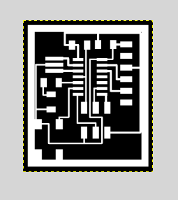
Now I created a new layer with white background and I gave it an inner black border of 20px, so I had my outline file

Milling the board
To mill the board I used the same procedure I followed in week4
And this is my board.
Programming the board
After I've soldered components and checked connections with the voltmeter, I tryed to programm the board
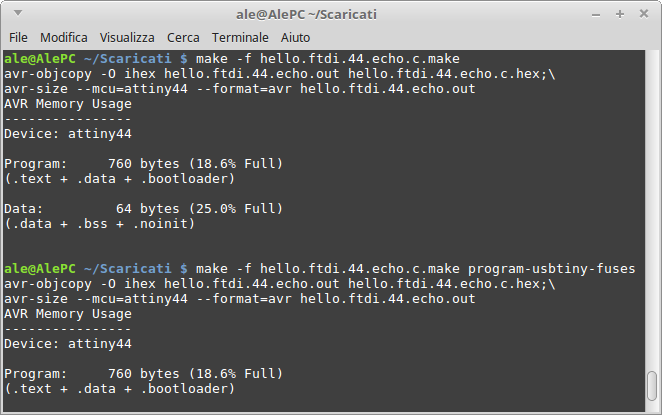
But when I moved to set fuses I recieved an error
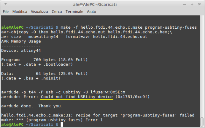
The problem seems to be that the USBtiny device is not found. To be sure I tried to found it through the "lsusb" command
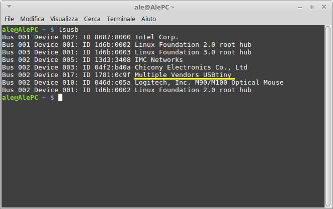
This time it have been found... But I wasn't able to go on in that moment. It was a bit confusing to manage all those things (new to me) at the same time, and at the end of the day the board was not programmed yet...
Update
During the following weeks I had other opportunities to study how to program a microcontroller, and I finally succeded for the first time at week 8
Eagle and program files here