Redraw the "Hello World Board"
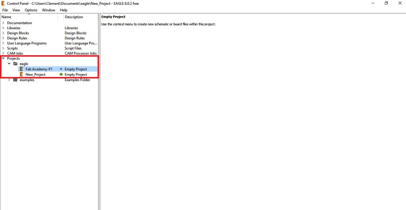
To redraw the hello world board I will be using EAGLE. THe first step is to download the software. What is EAGLE? It is and abbreviation for (Easy Applicable Graphical Layout Editor). It is flexible Electronic Design Automation (EDA) application with schematic capture editor, Printed Circuit Board (PCB) layout editor and auto-router. I downloaded Eagle on my Windows-10 OS and opted for the freeware student option. Follow the link to download student version of EAGLE
http://www.autodesk.com/products/eagle/overview
Eagle has an installer, run it.
After you install the application and open it, Eagle will ask you which version you want to install - choose "Freeware"
Once the installation is done get started with the drawing of the "Hello World" Board with EAGLE.
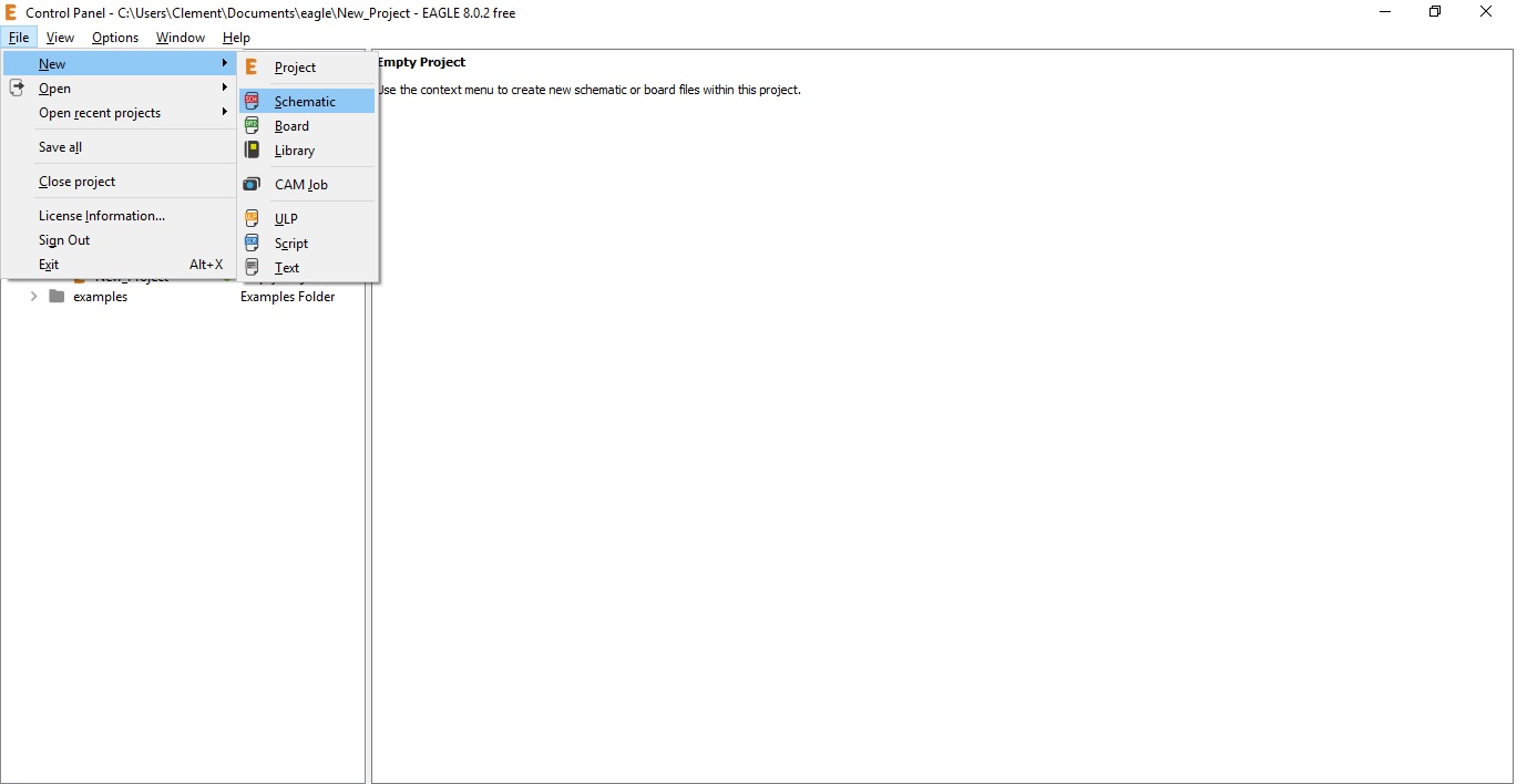
The next step is to prepare the schematic of the board. Those who have used AutoCAD will find it easier to work with EAGLE.
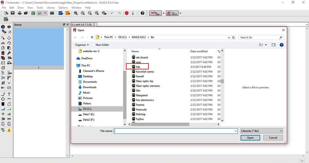
First we need to know if the components required for making the schematic of "Hello World" are there in the Library of EAGLE or no. If the components are not available then we need to download the fab library of the components required. Re-locate the library to the Directory where EAGLE is installed.
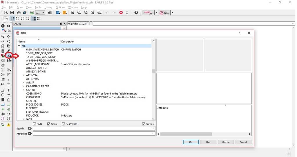
Components can be added by clicking the add button on the left tool bar and choosing the components from the drop-down menu. Now that's how I've got a basic idea how eagle works, I decided to complete this assignment to add a button and LED to Neil's board.Once all the components required are in the library, start creating the schematic by carefully following the diagram. The components required for the circuit are as below:
- ATTINY44-SSU x 1
- LEDFAB1206 x 1
- CAP-US1206FAB x 1
- RES-US1206FAB / 100k x 1
- RES-US1206FAB / 10K x 2
- FTDI-SMD-HEADER / 1X06SMD x 1
- 6MM_SWITCH x 1
- RESONATOR 20 M x 1
- AVRISPSMD / 2X03SMD x 1
Here below I have included images for a tutorial taught by Mr. Ayush
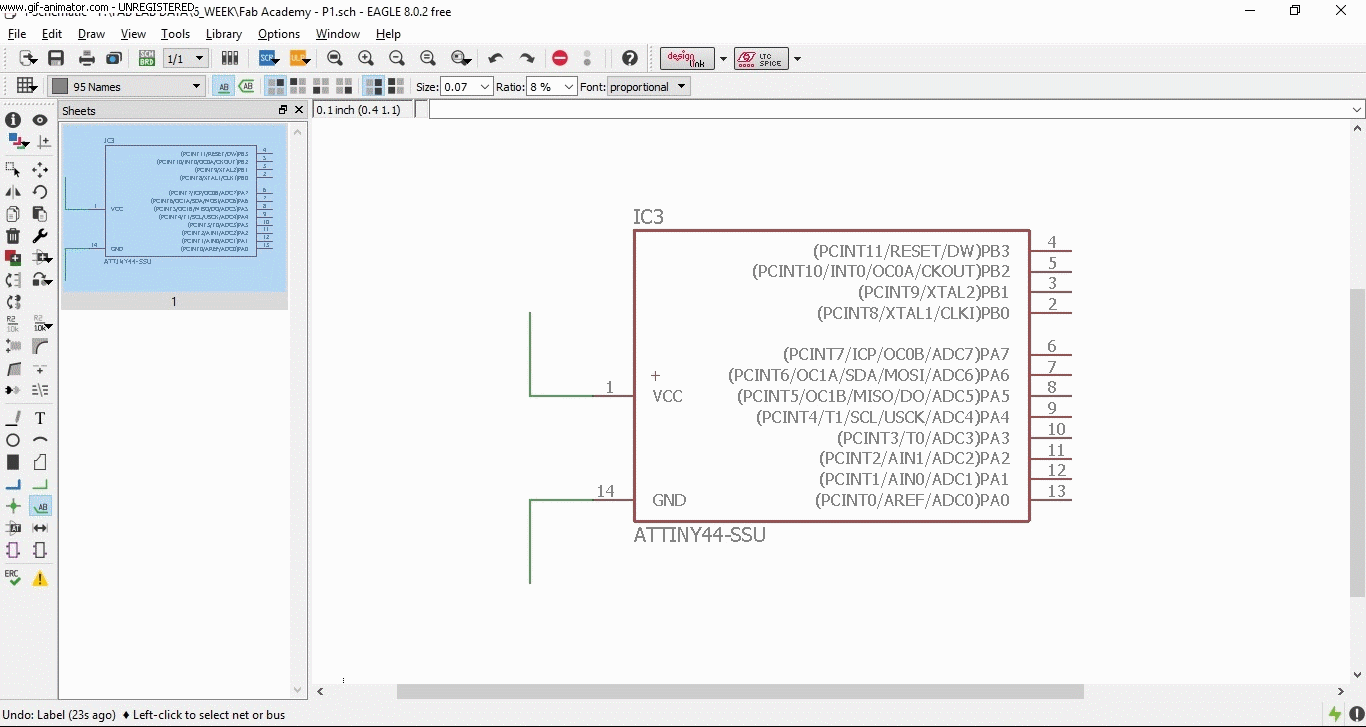
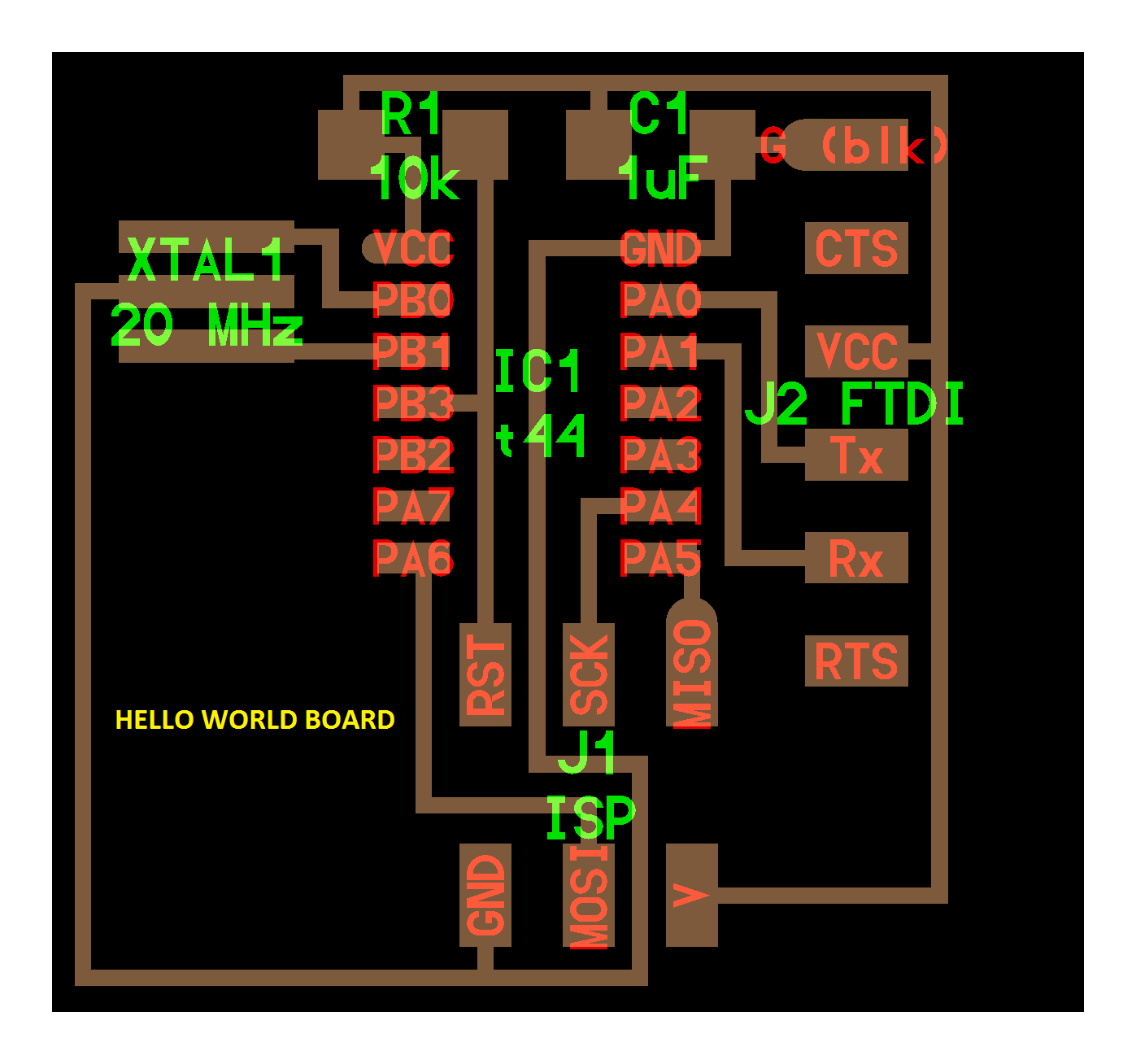
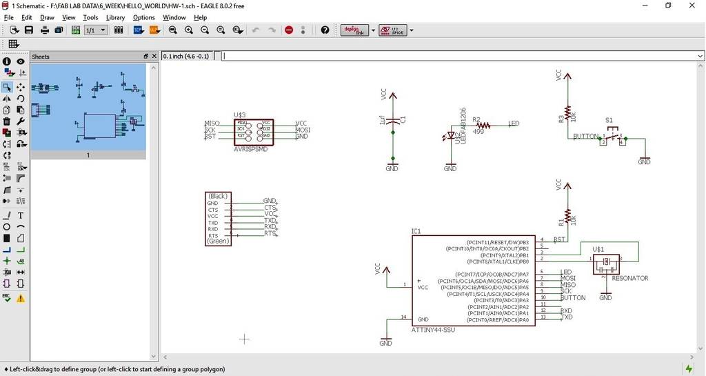
After I got used to work on EAGLE, I started building the schematic of "Hello World" Board. The final output of the schematic is shown below.
Since I was doing the electronics design for the first time it was difficult to understand the basics of the subject. But there are very good tutorials & literature how to make a good schematic. Follow the link below for the tutorial of "Hello World". http://fabacademy.org/archives/2015/doc/electronics_design_eagle.html#download_and_install_eagle
Once the schematic is completed , we can check for any errors or warnings in the schematic preparation by clicking the "Yellow" icon as shown below
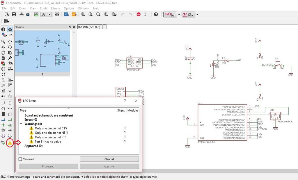
If there are no errors, Ignore the warnings & move ahead to the board layout by clicking the icon as shown below

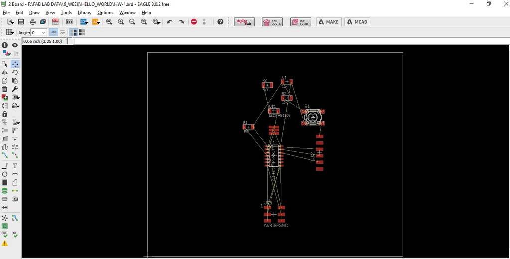
The window as shown will open with all the components displayed with the routing lines in yellow color.
I am creating a single layer board. So select only the "1 Top" option before using the "AutoRouter" option to create the traces of board layout.

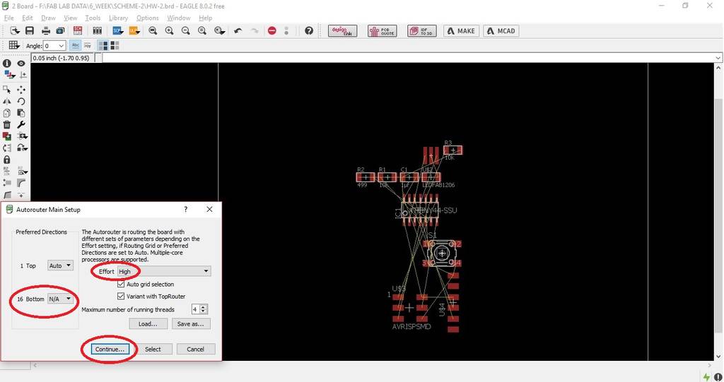
After doing this click on the "AutoRouter" icon as shown & the window pops up.
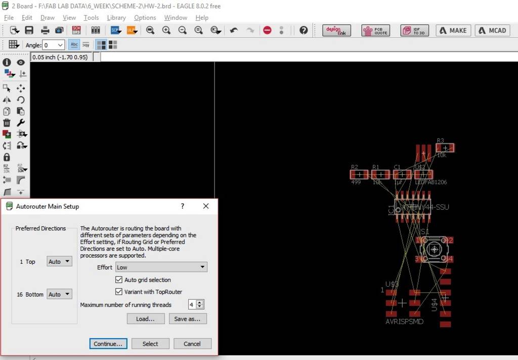
Change the settings to 16 Bottom - N/A & Effort to High & then click Continue
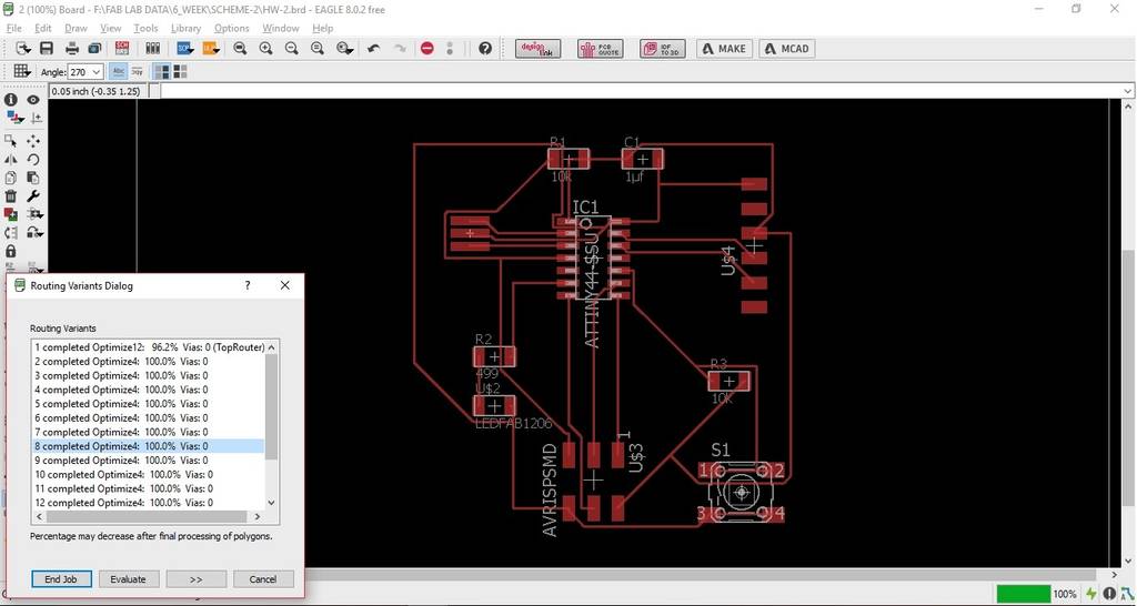
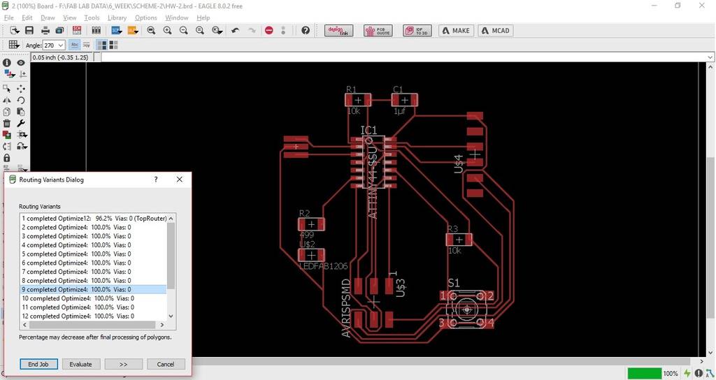
After clicking Continue the below shown window is displayed. Press the start button for creating many option of traces.
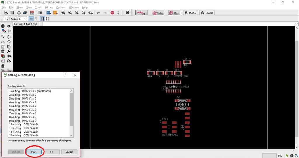
EAGLE works out many options of traces and displays us the results where 100% routing is done & also in-completed routing is done. Below are the different routing options created by EAGLE.
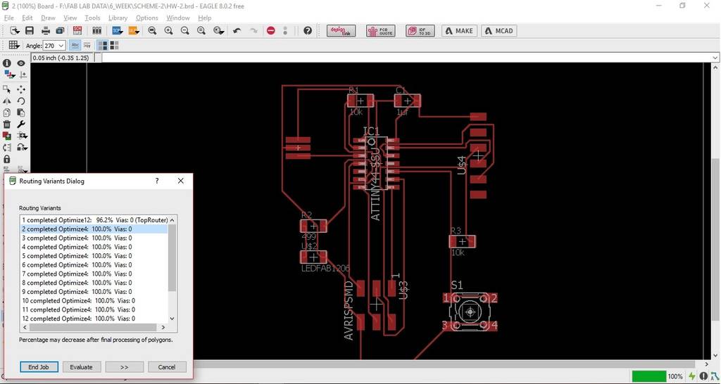
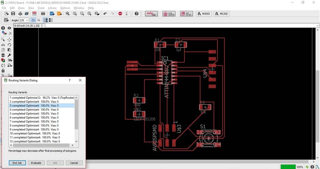
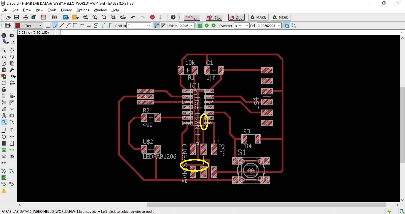
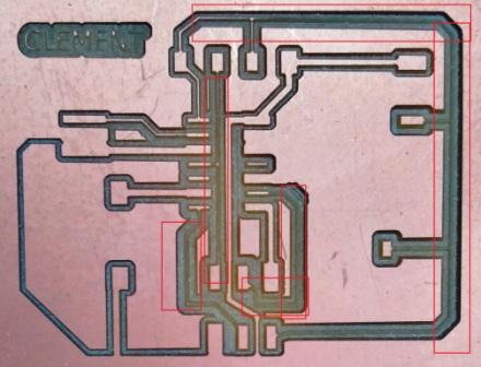
Here we need to check the best routing option where there are no traces going below the Resistors or Capacitors or the IC or passing in between 2 pins of the IC or any other component as shown below
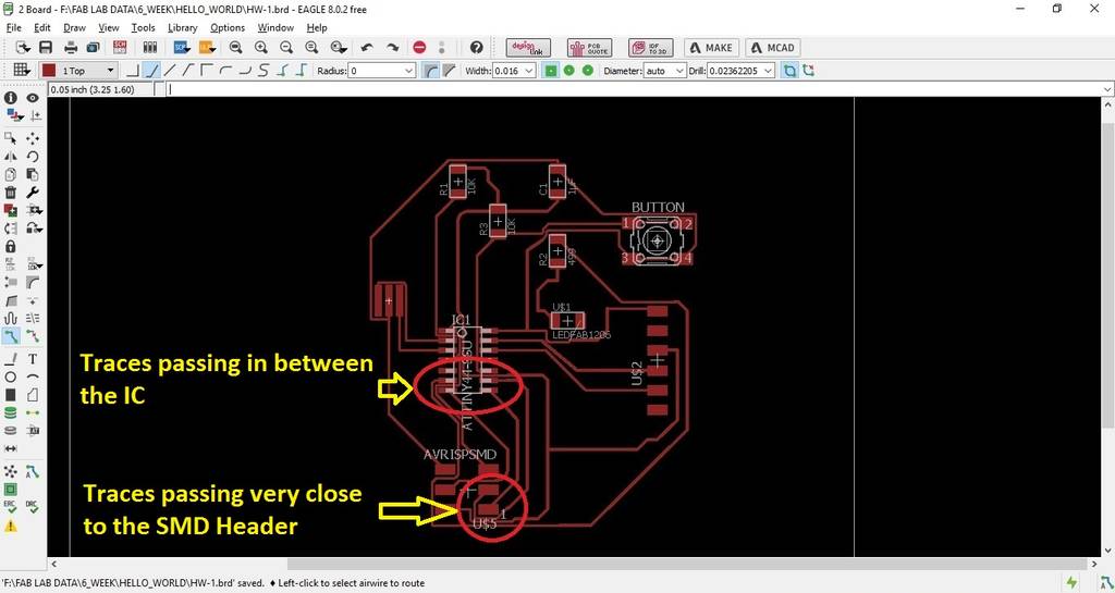
With these traces passing very close to the components will be difficult to mill the board & also to solder the components to the board. Hence its very important to select an option of trace which is cluster free and easy to mill & solder. At start its very difficult & tedious job to come out with a trace which is easy to mill & solder. A sample trace that I exported to .png file to check how it looks
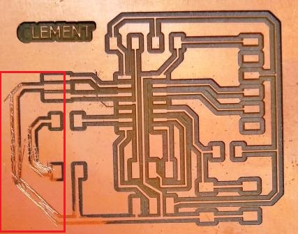
I re-arranged all the components again to optimize the traces and came up with this layout. When I checked for any errors & warnings, there were 2 traces which were very close to the pads of the IC & SMD Header pin pad.
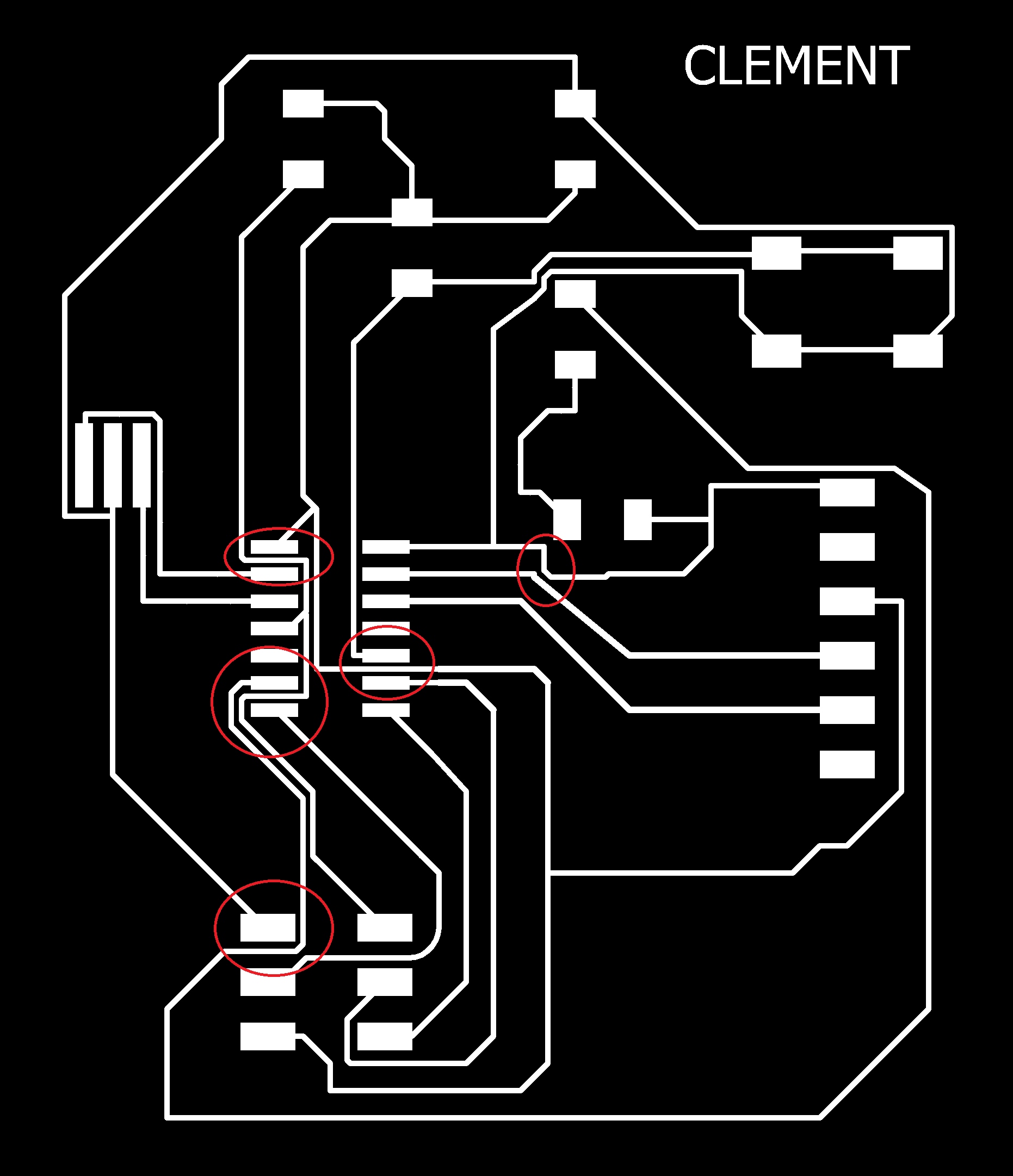
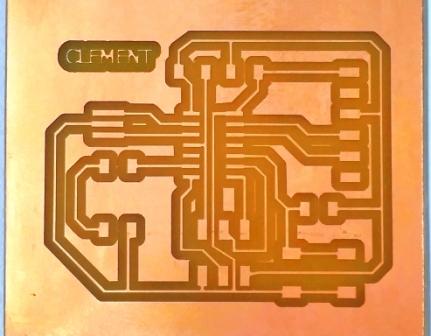
I did the manual routing & finally the trace layout as shown below is the feasible option
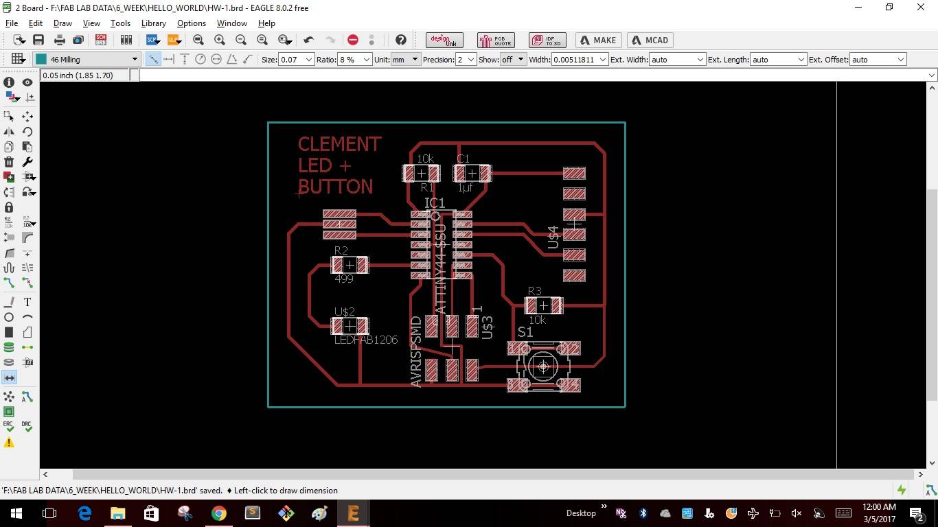
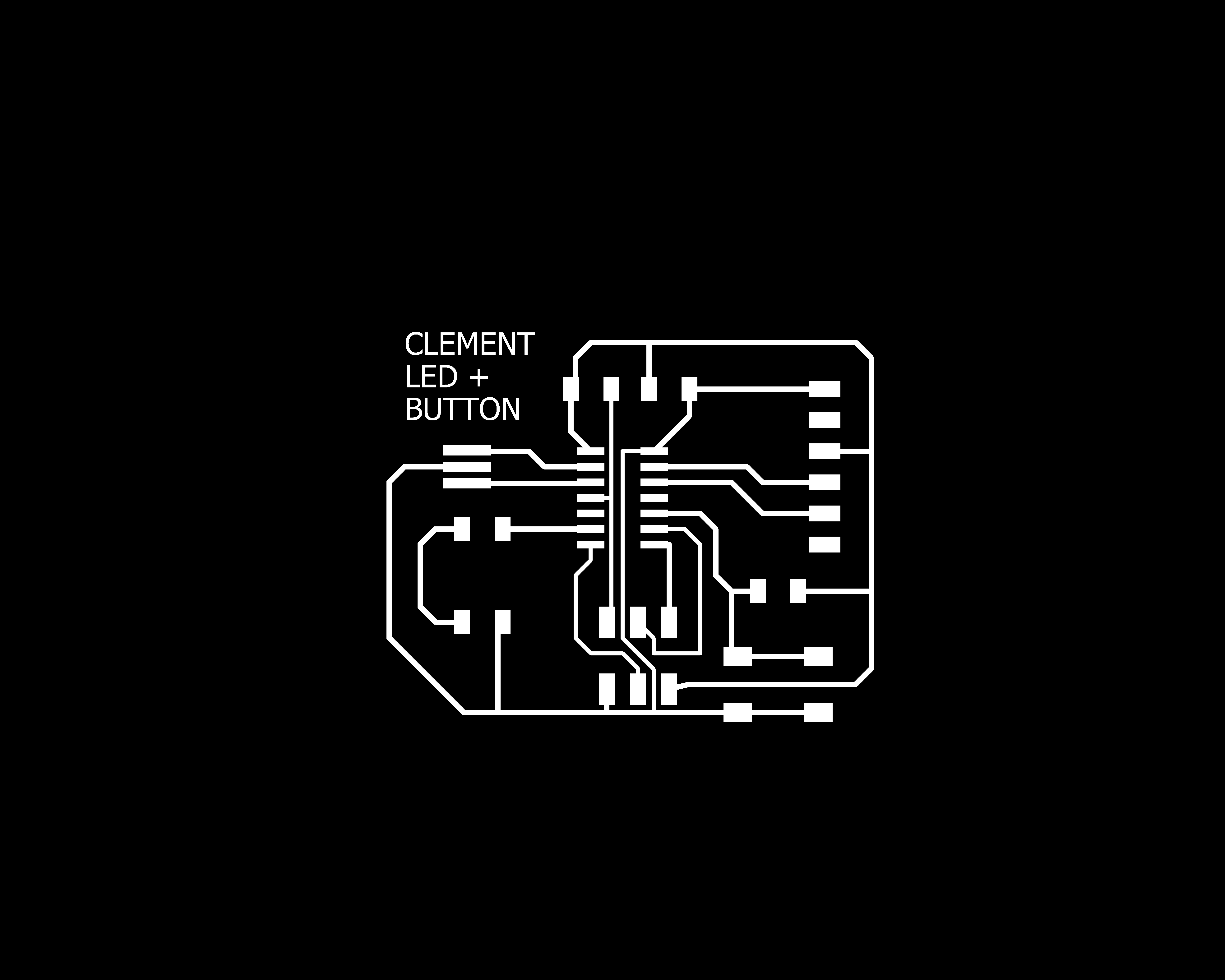
I exported the file to png format with 1000dpi & monochrome settings.

Problems Faced
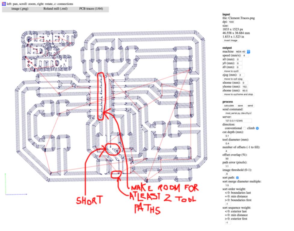
I imported the .png file to fab modules to create the .rml file and found that the tool path with 0.4mm cutter is giving an error as shown below,
The reason was that enough space was not provided in between traces & pads
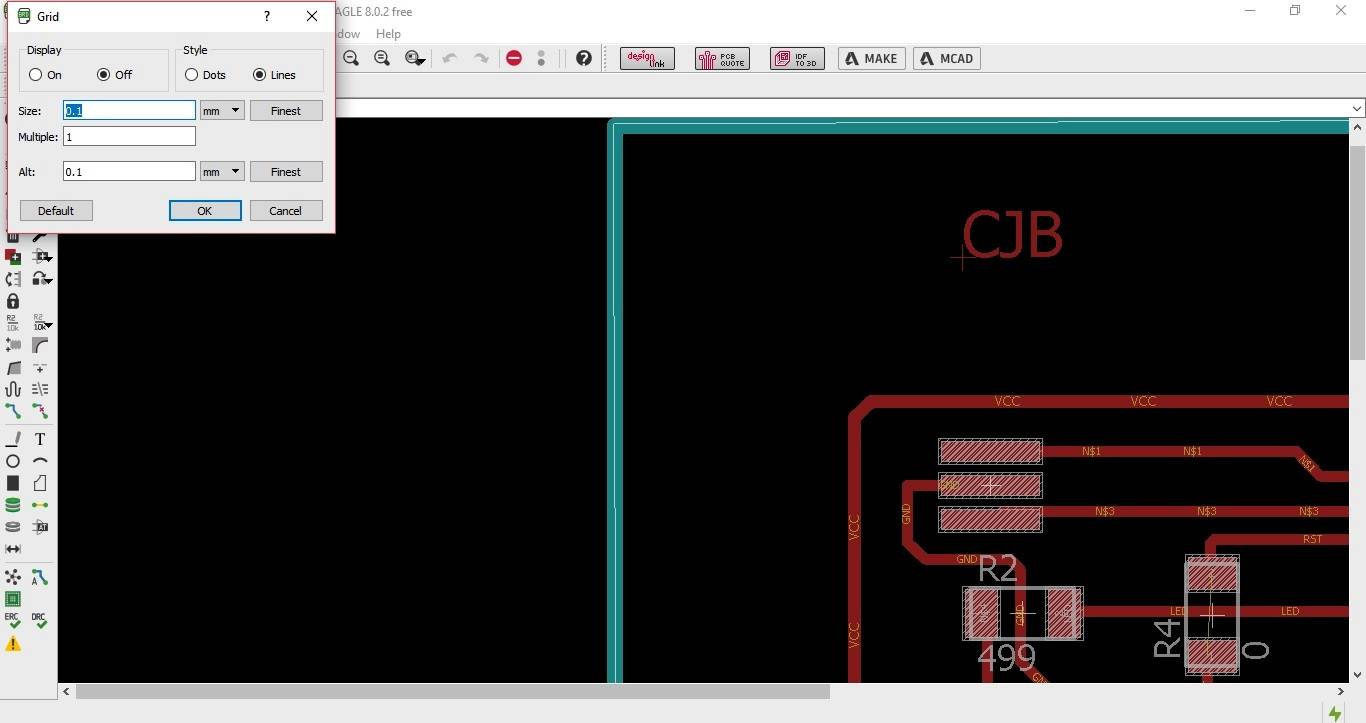
The default settings of dimensioning in Eagle are in inches. I was unaware of this setting before creating the .png file. After going through the details & following some literature I could change the settings of trace width & gap between the traces & pads. Below are some of the images showing setting changes in Eagle. Below image shows default grid width in "inches"
Below image shows how to change grid width to "mm"
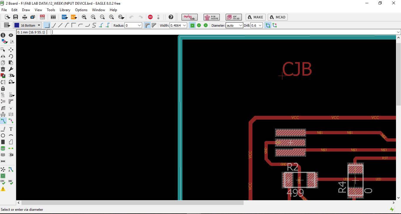
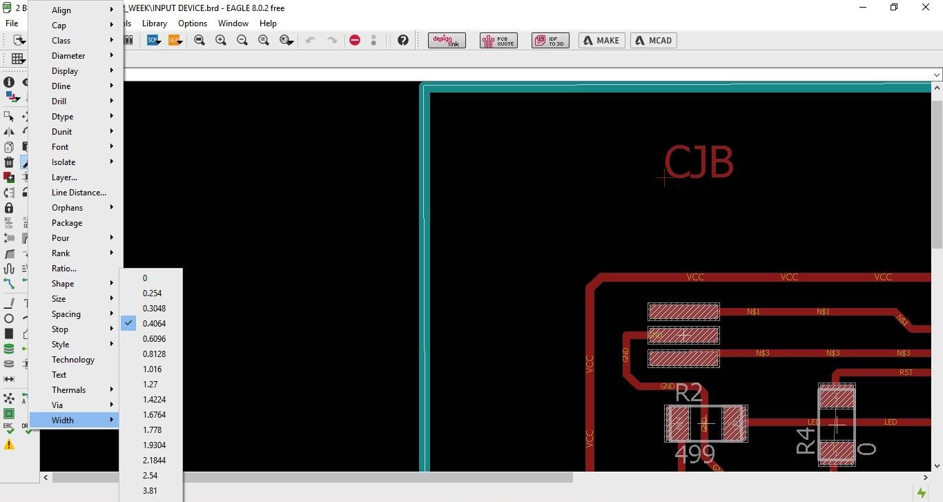
Below image shows how to change line width in Eagle.
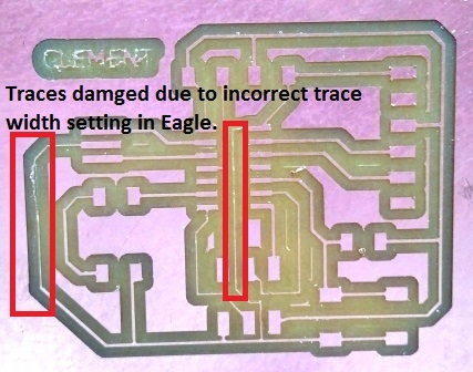
After doing these changes I started milling the board where I faced some different problems. The below image shows the traces damaged due to incorrect width setting in Eagle.
Below image shows the traces damaged, in fact completely removed because of using & setting cut depth of 0.2mm. Hence it always better to use "End-Mill Router for board milling.
Then I switched the "V Groove Router" to "End mill Router" and faced another problem of bed leveling. Hence it is always better to level the bed using "Dial Gauge Indicator" or spirit level before milling the board
Final Result
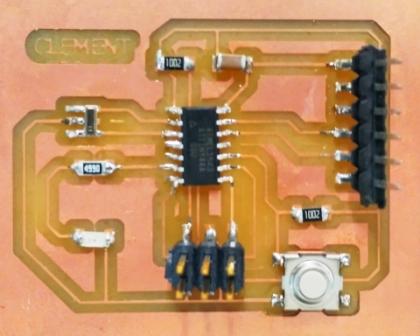
Finally after taking into consideration all learnings I successfully milled the board. Here all the traces are crisp & even.
Completed the Soldering of all the components on the "Hello World Board"
learnings of this week
- Learnt to use Eagle for designing schematics & boards using PCB's. There are many other softwares to design schematics, but I liked it very much because its very easy to understand. It has a good user friendly UI
- The Do's & Dont's during developing the circuits like track width, clearance between 2 traces etc,.
Files to download

This work is licensed under a Creative Commons Attribution-NonCommercial-ShareAlike 4.0 International License.