Study archive - Week 6
Electronics design
The lecture 6 on Wednesday 2.3 was about electronics design: how to design your circuit board, what components can be added and how to add them, and what SW can be used to create the schematic and design the board.
The tasks are 1) redraw the echo hello-world board; 2) add (at least) a button and LED (with current-limiting resistor); 3) check the design rules, and make it; 4) extra credit: simulate its operation; 5) extra credit: measure its operation. I describe below how I accomplished the first three tasks; the optional tasks of simulation and measurement remain for future work.
1) Redraw the echo hello-world board
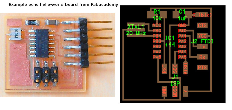
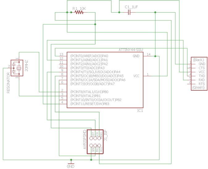
The echo hello-world board consists of a microprocessor Attiny44 (IC1 t44), a crystal resonator (XTAL1 20 Mhz), a resistor (R1, 10k ohm), a capacitor (C1, 1uF), an USB serial port (J2 FTDI), and an ISP connector for programming the board (J1 ISP). The files showing the board assembly and the board layout were downloaded from fabacademy lecture on embededed programming (see host communication topic).
For drawing the circuit board I have used Eagle (Easily Applicable Graphical Layout Editor), Version 7.5.0 for Windows (64 bit), Light Edition - a free version for "non-profit" (educational) and evaluation purposes. I found the tool very useful and quite easy to use after basic training and exercising, and once you know what you have to do. To add components I have also installed the fab library fab.lbr (by saving it from the Electronics design lecture page into the Eagle local folder, C:\EAGLE-7.5.0\lbr). This library contains all the components needed to design and produce the board.
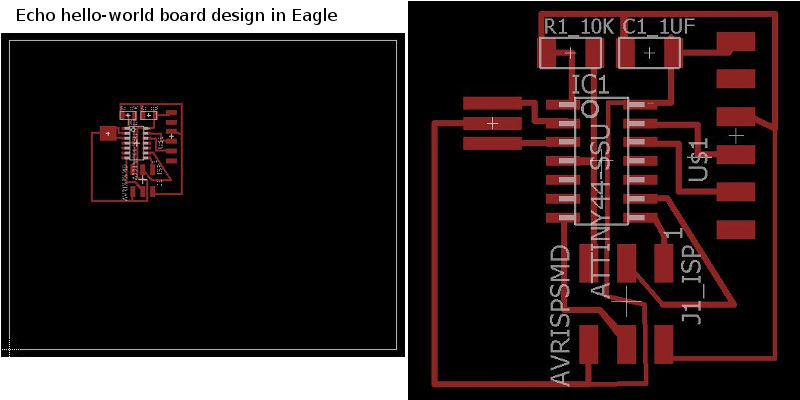
The final design of the circuit board is shown below (left: original size; right: enlarged image).
In the following I explain the workflow in Eagle. First I have created the circuit schematic, and then I created the board design.
Creating the schematic
The schematic contains all the needed components and the links between them. The layout of the components at this step is not so relevant, all that's matter is accuracy of the links (including the pin-level connections that are learned from data sheets) and the readability of the schematic. The schematic is used further to place the components at the assembly phase (e.g., how a led is oriented or how a button is oriented and connected on the board).
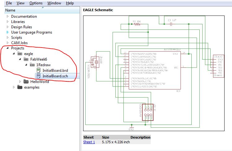
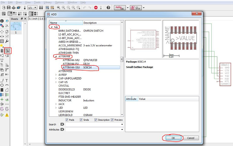
In the tree, in Projects/eagle folder I created a new folder FabWeek6 and within it a new project Redraw. In this new project I created a new schematic saved as InitialBoard.sch. In the Schematic editor window I have added the needed components from fab.lbr using the "Add" button. The following components were added: ATTINY 44 -SSU SOIC14, Resonator, Res-US1206Fab R1206FAB, Cap-unpolarized C1206Fab, FTDI-SMD-Header, and the programming 6-pin set AVRISPSMD 2x03SMD.
For connecting the components, I have used the button "Net". I have drawn paths between components based on the layout provided in the example board. In the schematic, it is ok to have intersecting lines; an intersection does not mean a connection unless the intersection is marked by a dot. One can also connect two components by simply naming the connection lines with the same name, without drawing the full paths between components.
Other tools that I used in the process were: Move, Rotate, Group, Delete and Name. Tools that I found also useful were Value and Split. The final schematic is shown below.
Creating the board design
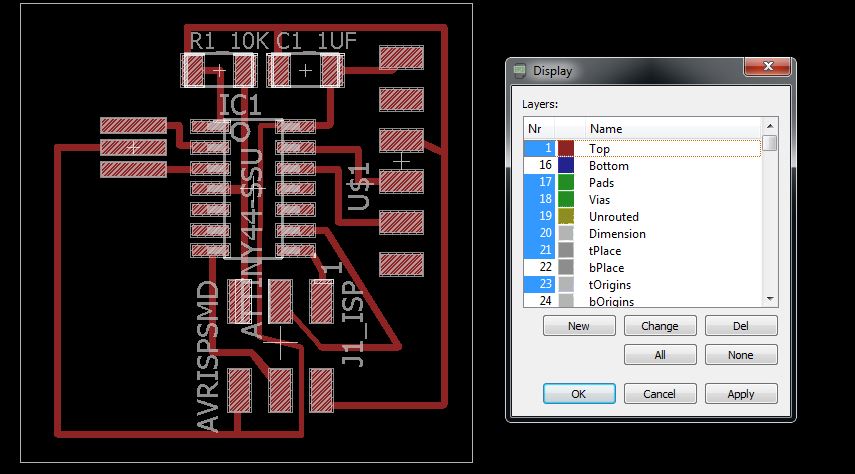
The design of the board is done in the Board editor window and the file created thereby has extension .brd (In the Schematic window, File > Switch to Board or click the switch to board button). First, I moved one by one the components to the board area. The connections are marked by yellow lines. I have used the button "Route" to draw the connections between the components. I have used the button "Change" to increase Width of route to 0.4064 mm. When necessary I changed the bend style of the route using right click or the buttons on the tool bar. To draw the routes with high precision press Alt key while drawing/moving the route. The Alt value can be set in View > Grid > Alt. At finish, I have checked the design rules by selecting DRC. The settings for Clearance define a check of the space between the pads and routes (wires) or between routes; the recommended value is 16mil (1 mil = 1/1000 inch). Because there were many conflicts (about 12) I had to correct the board: I changed some routes as well as the width between problematic routes to 0.3048. Thus, my design of the echo hello-world board differs a bit in the routes layout. The final step in the design was to resize the board area (the white rectangle contour) to fit the design; see below the final board with a different view (View > Layer settings ...).
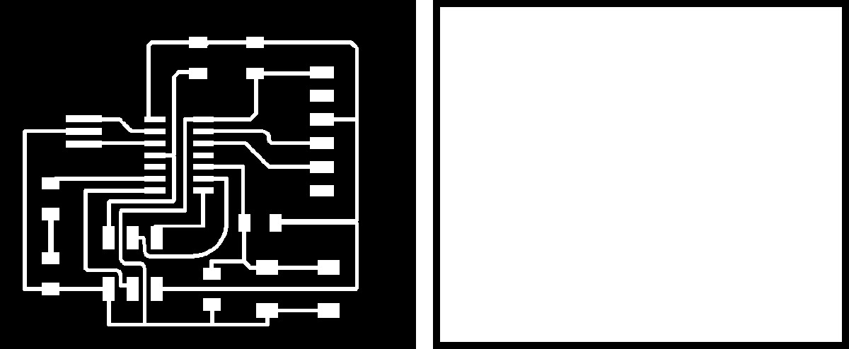
Creating the traces and outline in GIMP
For this, I followed the procedure described by Antti.
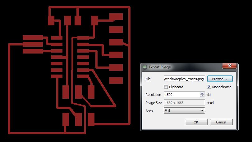
1. Export the top layer design from Eagle into an image .png with resolution 1500 dpi and monochrome (View > Layer settings ... > None; 1: Top and then File > Export as...).
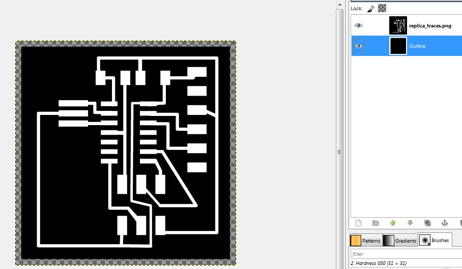
2. Open the image in Gimp and create a new layer with foreground color black. This new layer is for the outline.
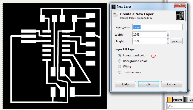
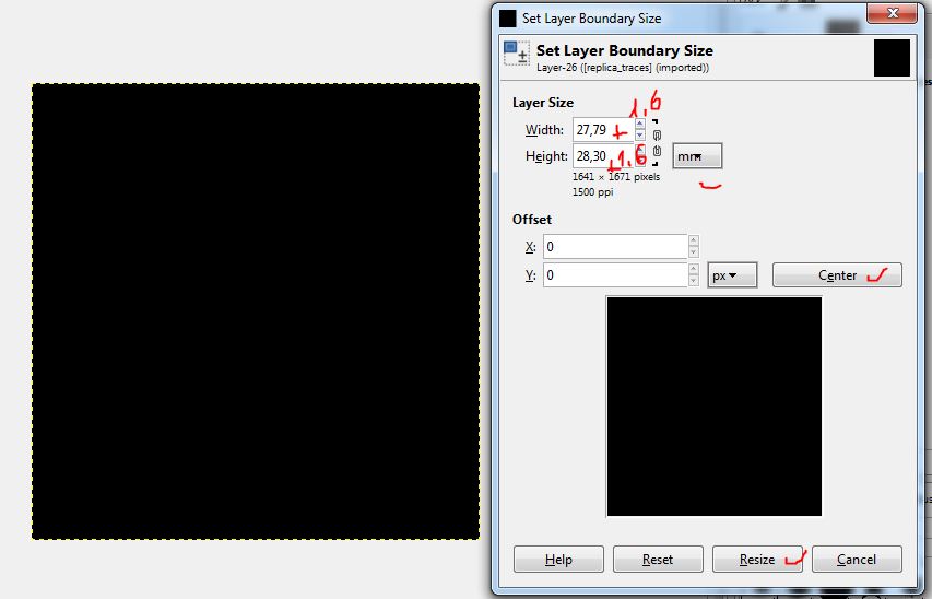
3. Set Layer Boundary Size for the outline layer by adding 1.6 mm to width and height centered. This is the margin milled away by the machine with the 1/32 bit (2,54 inch/32 = 0.8 mm).
4. Change the order of the layers in the Layers tab: on top the traces layer, and below the outline layer.
5. Enlarge the image to fit all layers: Image > Fit canvas to layers. And then fill the empty area with black.
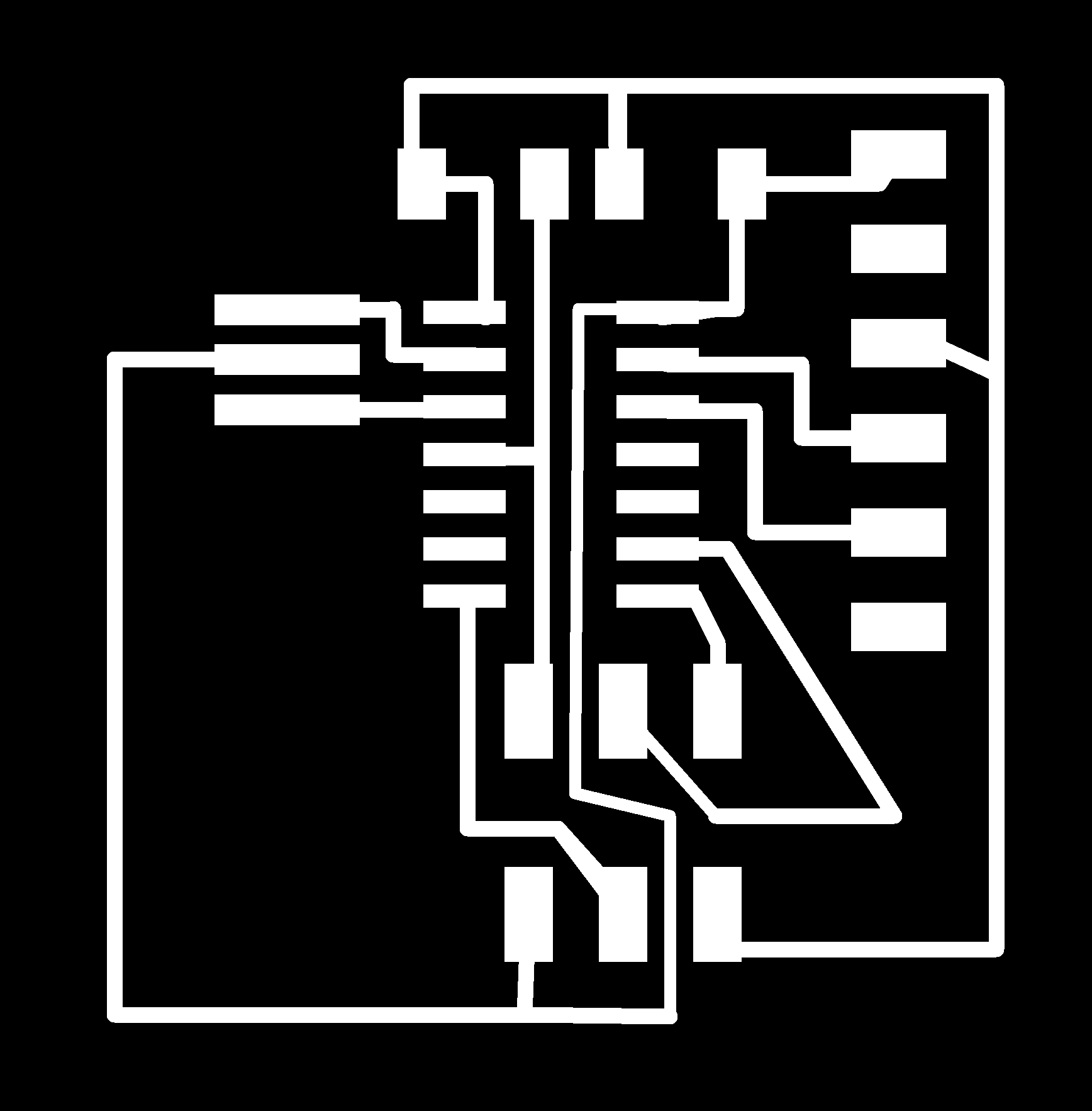
6. To create the traces image file, export the image as .png.
7. To create the cutout image file, fill the traces layer with white and export the obtained image as .png.

Summary of redrawing task
- Having a model board and design makes the design task in Eagle relatively easy.
- Feedback from experienced electronics designers (Antti, Juha, Jani) was very valuable: I've learned the following:
- my design was quite ugly (the angles smaller than 90 degrees are not recommended)
- the margin on the right-hand side of the board area should have been further away from the FTDI component to accommodate it better
- to draw both the schematic and board starting from the origin mark
- ERC function in Eagle is important to check the electronic rules of the circuit schematic
- the GND connection from the crystal resonator to the microcontroller and FTDI is quite long (causing unnecessary radiation); however for a small board like this, it is ok.
- When correcting the issues with the board, I've learned new things in Eagle and about electronics design: I have used more functions and tools: View > Layer settings - to select certain layers; Show - from button or command line (both in Schematic and Board) to see a path; Info - to get info about a component; Group - to select a group of components and paths so they can be moved at once; Label - to label a connection; Ripup - to reconstruct a path in the board design, Ratsnest - to reset the airwires to their shortest routes.
2) Add more components to the board (e.g., LED and button)
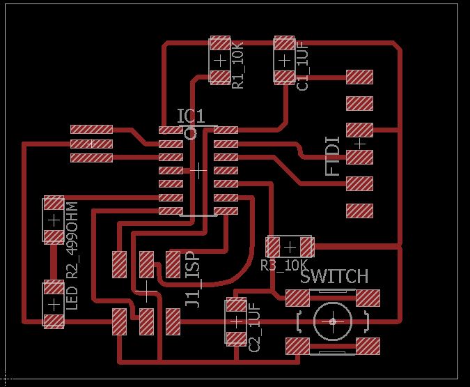
For this task I have used the corrected board according with the issues discovered during various feedback checkpoints with my colleagues. This task was iterative: 1. I have added first the led, the 499 ohm resistor, the button and the 10k ohm resistor and I designed the board with care. However, both the led and the button were not connected to the microcontroller. I completely overlooked this aspect when drawing the schematic. 2. Thus, I had to update the schematic and connect the led with PA7 and the button with PA3 (this info was in Fabacademy tutorial, see the link at the end of the page). 3. Next I have designed the board and when I was again ready to print it, I asked a second opinion from Antti and he suggested me to add a capacitor in parallel to the button to overcome transient. 4. So here I am designing for the third time the board. But the result is good and so the learning.
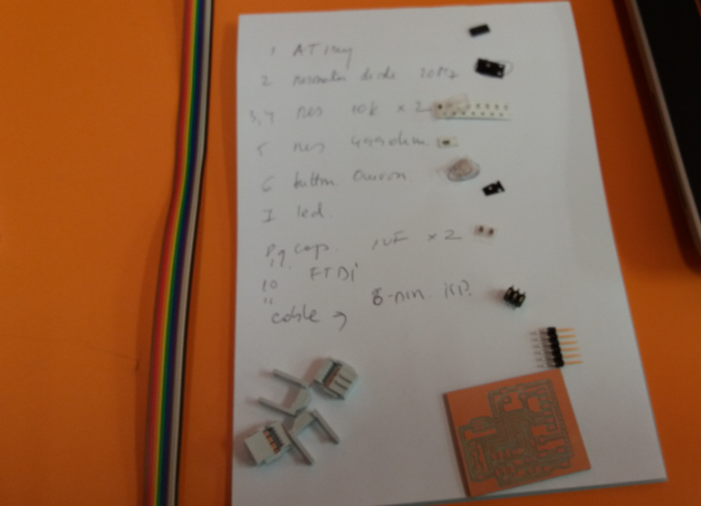
The final board contains the following components from fab.lbr:
- Microcontroller ATTINY 44 -SSU SOIC14
- Crystal Resonator, 20 Mhz
- Two resistors Res-US1206Fab R1206FAB, 10 k ohm
- Resistor Res-US1206Fab R1206FAB, 499 ohm
- Two capacitors Cap-unpolarized C1206Fab, 1uF
- FTDI-SMD-Header
- 6-pin set AVRISPSMD 2x03SMD for programming
- Button 6MM_SWITCH6MM_SWITCH, Omron Switch
- Led LEDFAB1206 (Orange clear)
In the schematic I have also added two componets from Supply 1 library, namely GND and VCC for representing the connections with the ground and power, respectively.
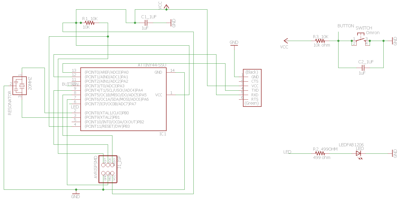
The final schematic is presented below. Observe that the led symbol has a line in one end which is connected to the GND. This should be kept in mind when assembling the board: the physical led component has a line (e.g., green) at one end representing the cathode which should be placed on the board accordingly (the line to be connected with the ground).
The ERC (Electronic rules check) was used at this point to check for errors or warnings regarding the working of the circuit board. The following issues were identified and corrected: missing values for resistors and capacitors, too close connections that had to be redrawn, missing visual connections (corrected using Label for the path).
For the board design, I have used File > Switch to Board to open the Board editor. Here I used Group and Move Group to move all the components inside the board area. Manually I have used the Route tool to connect the components. The width was set to 0.016 inch (0.4064 mm). Finding the right paths is quite challenging. I have used inspiration from the tutorial example, but I've tried also to add my own design. The picture below shows the board design.
3) Check the design rules and make the board
The design rules were checked with DRC and setting the clearance parameters to 16 mil for Pads and Routes; all other parameters were set to default values. Among the revealed problems were an overlap and a few too close connections. After these were fixed, the board design was exported as .png file to be processed in GIMP.
In GIMP I created the cutout and traces .png files for the milling by using the procedure described earlier at task 1). The results are presented below.
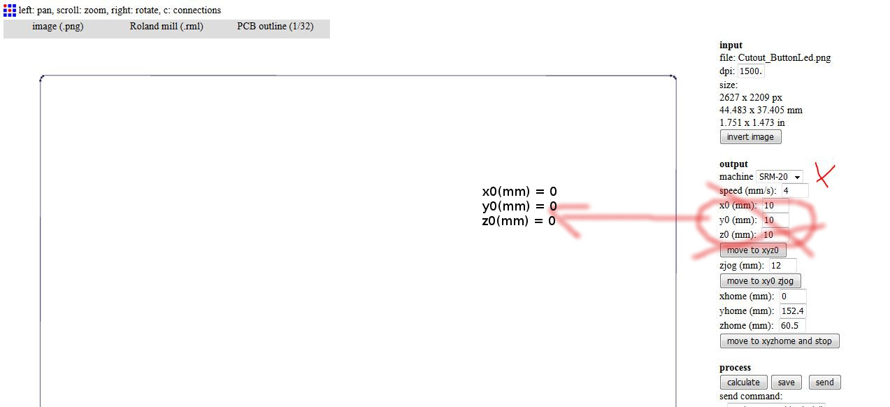
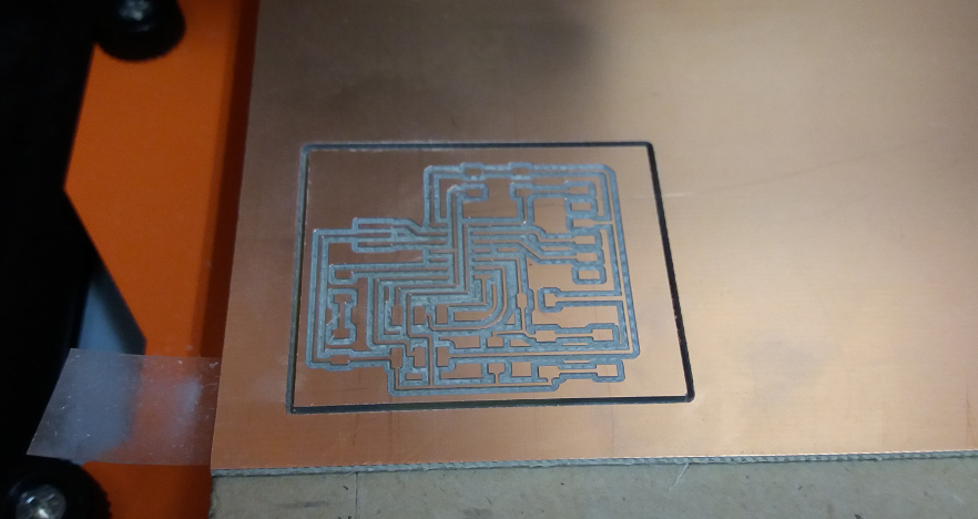
For milling, three .rml files are created using the fabmodules.org and they are used in the VPanel to mill the board. At this time, when running the test tracing of the outline, the parameters for the output coordinates in the fabmodules were not set right (instead of 0 were 10 mm), and thus tracing job did not reach the board. This was a good learning experience to remember the meaning of the output parameters. The same steps as described in Electronic production page in the study archive were done. The result of milling is shown below.
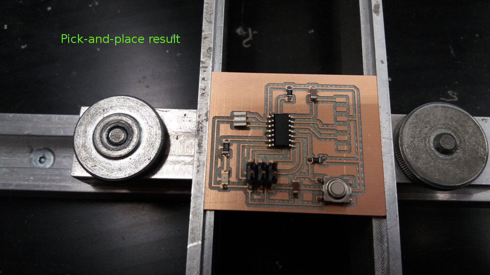
For assembling the parts on the board, the components are selected and marked on a paper when found. This practice can also help as a reference when soldering.
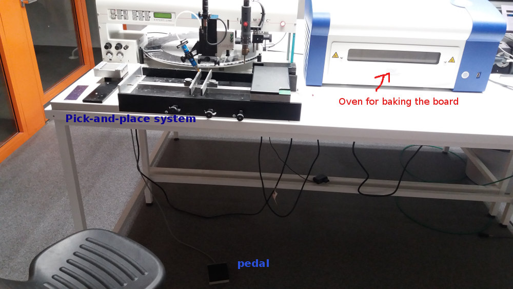
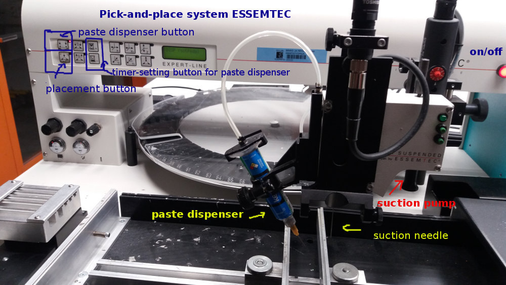
This time, I have done the soldering using a pick-and-place machine (Essemtec - expert line) and a special oven to bake the board (LPKF Protoflow) available at FabLab Oulu. This system is called surface mount technology (SMT) for placing components with high precision and efficiency (aka pick-and-place) and for soldering them on the board.
The process consists of:
- Apply soldering paste to pads.
- Press the paste dispenser button on the system interface (first button on the left on the top row).
- The paste dispenser needle is set to be lower than the vacuum needle (by dragging it down by hand).
- The dispenser is moved manually to the correct position on the pad.
- When the needle touches the pad, use pedal (once) to apply the paste on the pad (this corresponds to a timer set to 0.7 s). The operation can be done without using the pedal by setting the timer correctly, e.g., 0.7 s for pads designated for resistors and alike, and 0.5 s for microcontrollers pads. When the needle touches the pad will automatically put the paste on it. If you use pedal, after releasing the pedal, let the needle on the pad a bit more until all paste is put on the pad and the tip of the needle remains clean.
- Place the components on the pads using the suction system and needle (or nozzle).
- Set the position of the paste dispenser back to its place (higher than the suction needle).
- Press the placement button on the pick-an-place station (first button on the left on the bottom row) .
- Then place the components one at a time using the pump on the right side to control the suction and the direction of movement. When the component is on the correct place on the board release the suction pump.
- Not all components can be placed using this system. E.g., the FTDI connector was left aside to be soldered by hand.
- When placement is over, the pick-and-place machine can be shut down.
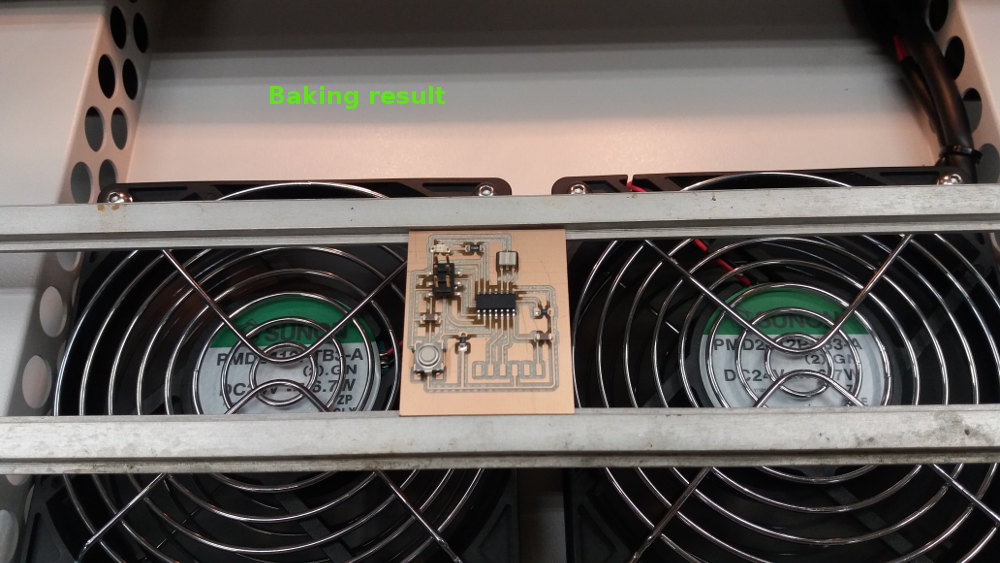
- Bake the board in the special oven. For operating the machine use the up-down arrows to select the options that are shown on the small screen and use the right arrow to press ENTER. The small blue screen shows options, status, and instructions.
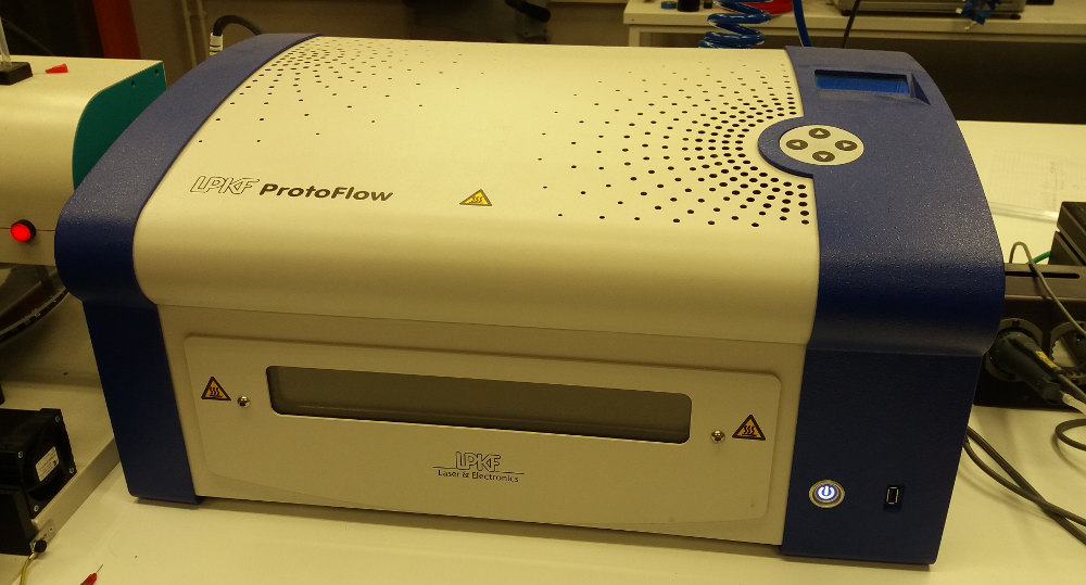
- Open the oven.
- Set the distance between the rails by placing the board on the rails in a loose way so that the board can be taken away easily when hot.
- Take away the board from the rails.
- Close the oven.
- Select the profile (Profile settings) as LF-Medium.
- Start profile for warming up the oven up to 160 C. When this is ready Press enter to insert the PCB.
- Place the PCB with care because the rails are hot; grab the middle of the board.
- Close the oven drawer (ENTER) and the system will preheat again for 2 min up to 160 C. Then for about 100 s it will reflow to 235 C.
- When reflow is ready, the oven opens automatically and cools down for 80 s.
- Then it is safe to remove the PCB and press enter to close the drawer.
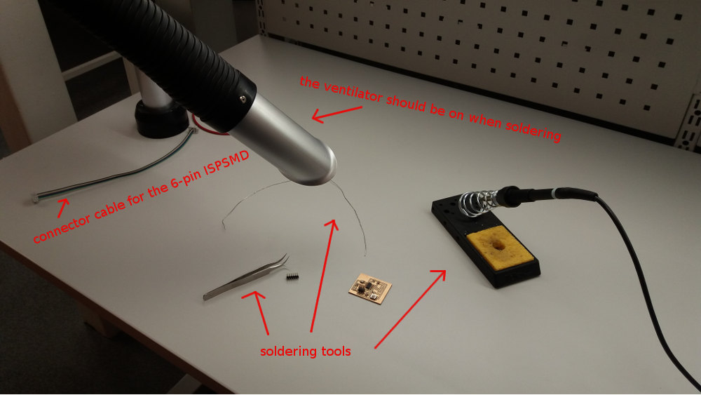
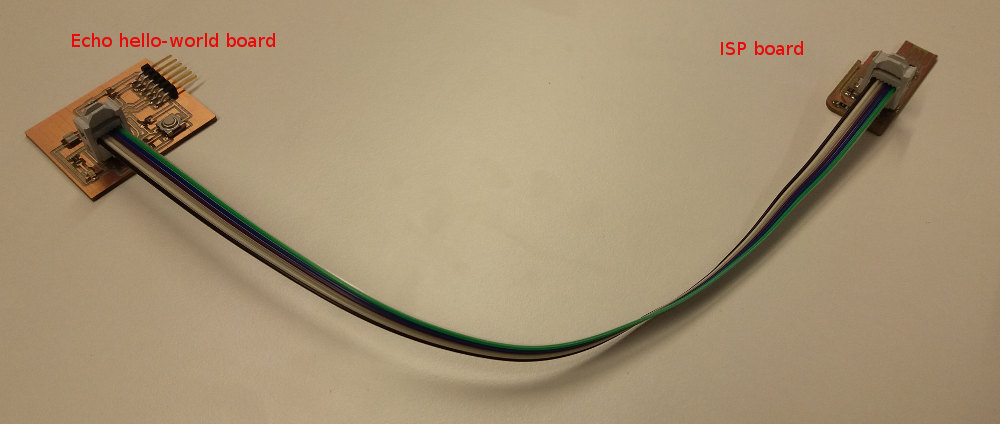
Next I have made the connection cable for the 6-pin ISPSMD and also solderd by hand the FTDI connector.
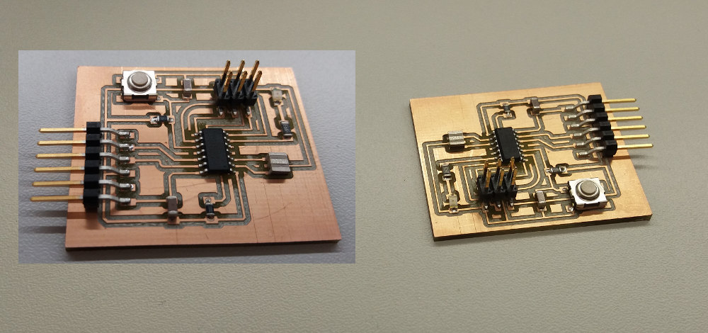
The final echo hello-world board assembly and the connection with the ISP programmer board are presented below.
Learning resources
For the electronic design tasks, I found the following online resources useful for learning:
- Eagle tutorial from Fabacademy
Summary of the week
- This week task was challenging, but interesting because I have not had contact with theory of electronics since my physics classes in highschool (more than 20 years ago). This was also my first hands-on experience with electronics design. Thus I found the tutorials in SparkFun good and easy.
- Eagle is a good SW for electronics design. I liked that it provides automatic alternative routes in the board design mode (e.g., by pressing on a pad and dragging the pointer it shows possible routes and it is then up to the designer to choose the route).
- The soldering with pick-and-place and the baking machines is really efficient and precise, and thus more fun than manual soldering.
Summary of Tools used
Software
Eagle - for design of circuit board
Gimp - for creating the image files
Fab.lbr - library of electronic components for design in Eagle
SW tools for the production step - see Electronics production archive (Fabmodules.org, VPanel)
Hardware
ESSEMTEC Expert line - pick-and-place machine
LPKF Protoflow - for baking the board affter pick-and-place process
See Electronics production archive for Milling machine, soldering workbench and tools
Source files for download
Eagle files (.sch and .brd)
GIMP files
Milling files (.rml)


