This week our assignment is to redraw the echo hello pub board and add at least one button and one led to the board.
I did a little bit research about what software members in Litchee Lab are using, and they said Altium. A nd then I chose this as my start point.
The reason our engineers suggested Altium is because Altium supports the whole process of PCB design. But as a beginner, I can not say my experience with this software is happy.
Check out the workspace. A lot of different menus and all buttons around make me feel this is another language...
However thanks to the bad internet access to 123D circuit.io, I stayed with Altium and learned some useful things after this week.

You can find more about Altium with the link of their website in the Reference part.
|| Schematic - part 1
A new project in Altium starts from schematic. To draw the schematic, you need to understand the BOM of your circuit board.
Here is the list of all components used in the echohello pcb board:
1) Attiny44 smd version
2) 0805 10k resistor x 2
3) 0805 1uF capacitor
4) 0805 1k resistor
5) 0805 led
6) 2 x 3 6 pin ISP header
7) 1 x 6 6 pin FTDI header
8) 20Mhz resonator
In the page of the assignment, Neil provided the picture of echo hello .pcb. The pictures are like:
(original pictures x 2)But they are not enough...
To redraw the board, you need to understand the package of each component you are going to use. The number 0805 in the list above represents the package information.
|| Build the library
Altium comes with two interior library in which you can find some common through hole components. Yes, through hole, which means nothing useful for our surface mount board.
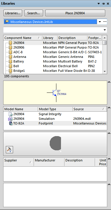
Then next challenge will be create my own library.
I tried research first. And I found the library of AVR chips. Then I downloaded and get my Attiny44 into the scheme.
You can find the link to the AVR library in the reference part also.
But for other parts, I decided to create my library, cause it seems not hard and interesting to do it.
A new component consists of a scheme and a PCB layout also. Start from scheme, you can draw any shape of the component and add pins to it. Below is the first component I created. However, something is wrong. What’s wrong? The name of the pin should stay on the body of the component, and the pin num stay on the pin.
so the correct one is like this:
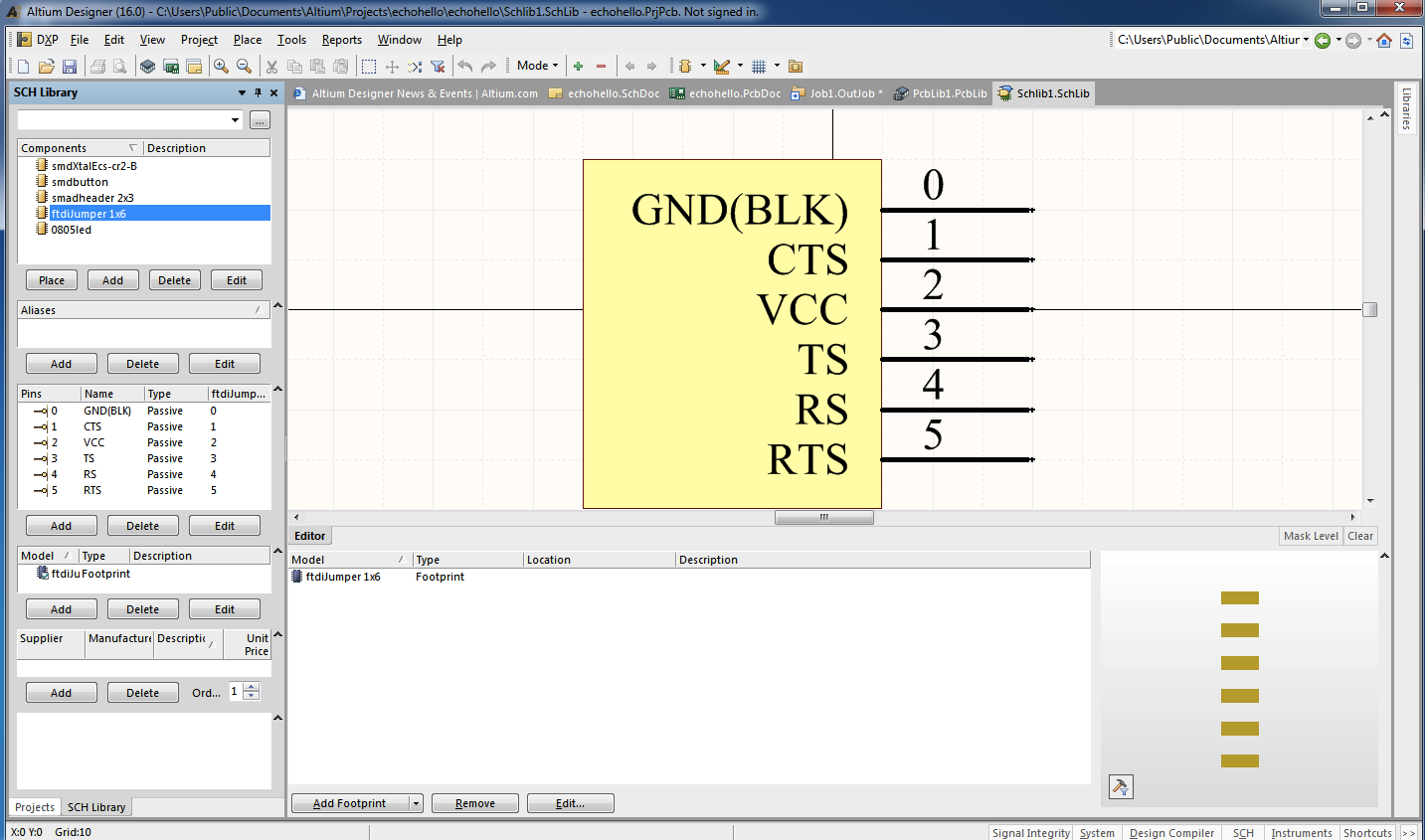
This is important. If you put them in the wrong positions, the final scheme including these parts can not be wired up appropriately.
After the drawing of the scheme, we can move to PCB layout. The drawing of PCB follows strictly the physical dimensions of the components. Datasheets can help with these data.
I attached the datasheets I found for this circuit board in the reference part also. If you are interested, you can go and check. So typically this part of the datasheet help:
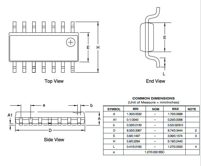
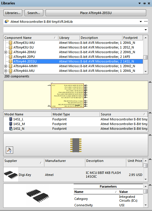
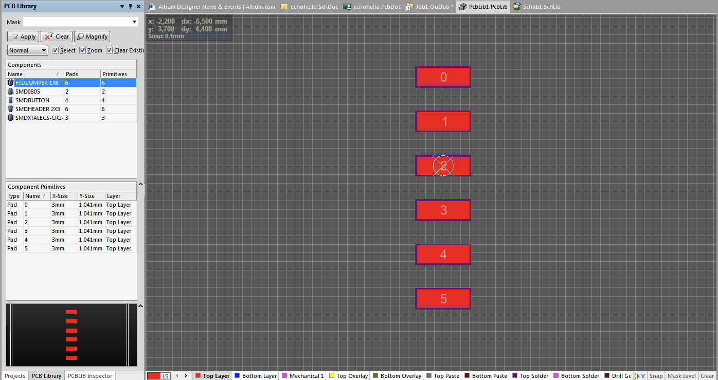
And this is the footprint of FTDI header. 6 pads for soldering.
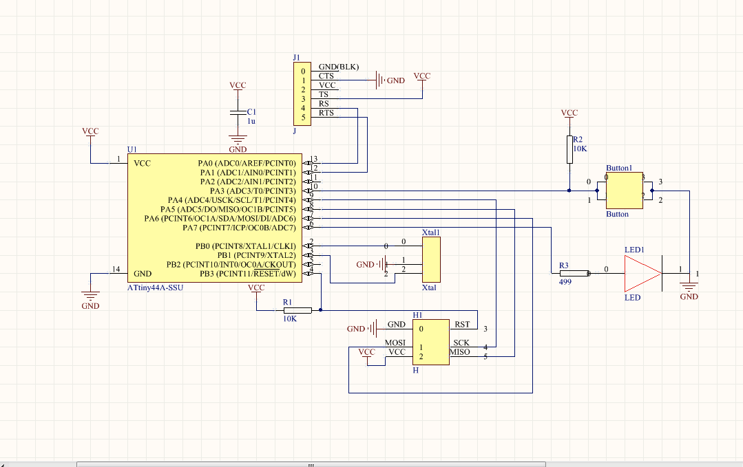
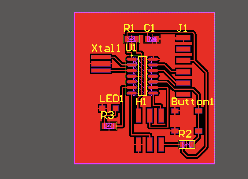
After creating all components used in the circuit, I wired up them all and got the schematic of the new board:
|| PCB layout
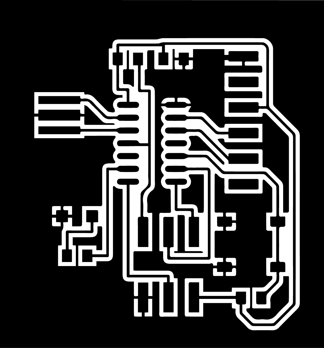
PCB layout is the next step. Create a new PCB file, and then route all wires. As long as you build all components right, then you will see all components in the PCB file connected together just like the scheme.
And routing wires is like a puzzle. Because we are going to use milling machine to mill a PCB board, so we can only route all wires on the top layer.
After a few time struggling, I made this:
|| Get the PNG file for Roland machine
For image, Altium can only output .pdf. So I did some modification in AI to get the PNG file for fab modules like below:

Feed it to Fab modules and then I got the .rml files for the roland machine.
The process of milling the PCB is just the same as W4. So I skipped it here.The board I got is not ideal. Some lines are too narrow to break. I tried several times changing the settings in Fab modules. And finally I think the design in Altium needs to be changed a bit. I did not have time to do this this week, so I left it later.
After soldering, I got this:
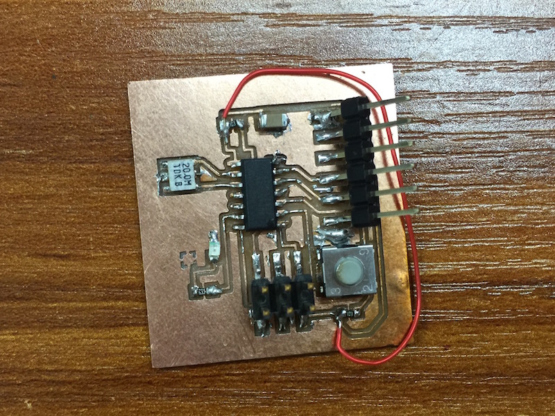
Some problems in this step also. The specs of components I got finally are not the same as I created the library. The lesson here is check the physical components before you created the library!