The aim for this week assignment was to redesign the Hello-World PCB board We also had to add two more components (LED and a button) incorporating its connections to our board. It was necessary to know how different programs work in order to design our board. I started using Eagle software.
I downloaded Eagle in my computer and as it was the first time using that program I follow the tutorial step by step. I also installed in my computer all the fabacademy libraries where I could found all the different components used in the curse. I also downloaded the rules for the milling machine, these rules are the ones that tells us what is not going to be milled or what is wrong in our board when checking it up.
For designing the board it is necessary to understand all the connections between the different components so that everything is clear when designing it, for this, we make a distinction between two different types of files:
The schematic (.sch): is a scheme of our board that tells you which element is connected to, what are the names for each element etc. The position of our elements in our schematic file may not be the same as the position in the board file, which is to say that the schematic file is used to see the connections within the board.
The board (.brd): is the final layout for our board. Considering all the connections in our scheme file we decided the best route that fit in our board. This file will be the one to be exported to .png format that we will send to the milling machine.
First of all I did a list of all the components in which I specify the name of the elements, the manufacturer part number, the description, price and link to the web-site in my case, I used Digi-Key.
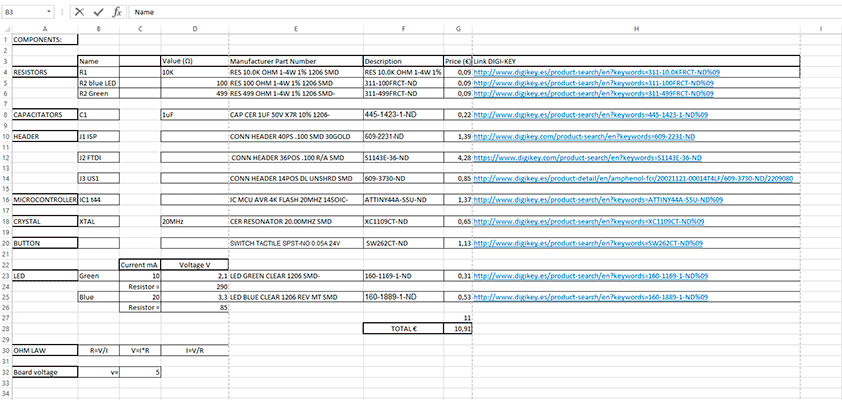
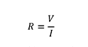
In the case of the LED I specified the voltage and the current to then calculate which resistor of what value was necessary. The value for the resistors are different depending on the LED colour. In my case I used a blue LED so I calculate the value of my resistor with the Ohm’s law: µ
SCHEMATIC PROJECT
I inserted all the components on my list in the schematic project:
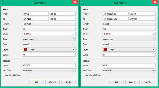
Resistor 1 : 10K
Resistor 2 : 100 Ω
Capacitator 1 : 1µf
Header 1 (FTDI) : 6 pin
Header 2 (ISP) : 6 pin
Header 3 (US1) : 4 pin
Resonator : 20MHz
What I did, was connecting them by labelling the routes and giving them the same name. When giving the same name to two different routes the program asks you if you what to connect them.
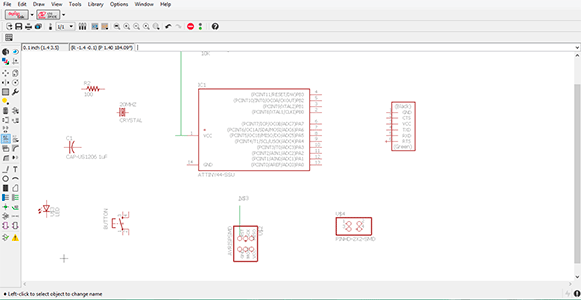
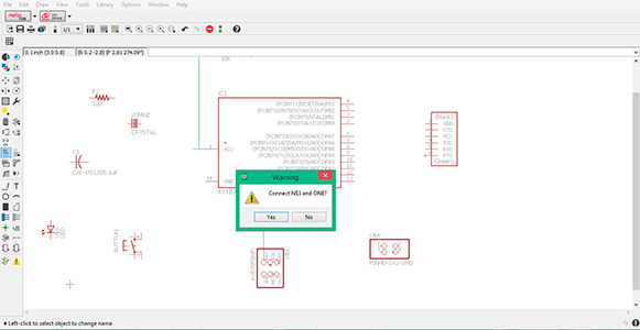
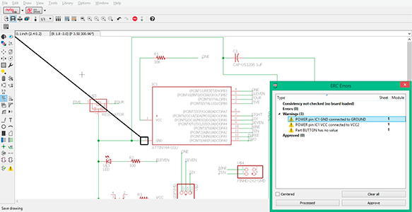
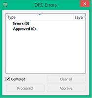
The connections for GROUND and VCC I did it with the net option so I had a clear scheme of my board.When I finished all the connections between elements, I checked if everything was right. I didn’t have any errors that means that it was correct. There were some warnings that weren’t important so I could approve them.
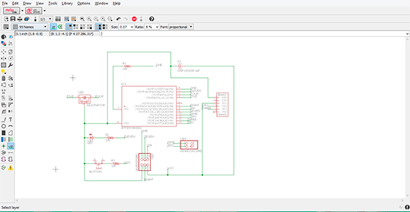
BOARD PROJECT
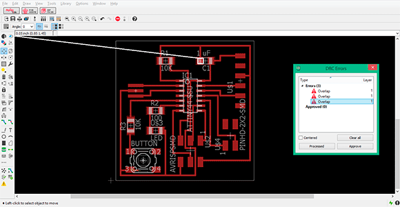
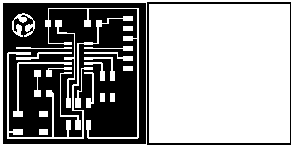
Once I finished the schematic project with all the connections I opened the board project. The yellow lines indicate which element is connected to. Considering all the connections in our scheme file we decided the best route that fit in our board.
Before starting to make the connections we must place all the elements inside the white square which indicates the area of the board. This margins can be modify depending on the size that we want our board to have.
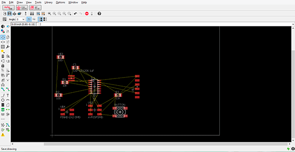
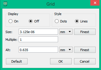
I had some problems with the vias under the microcontroller because they were very thick and were joined to each other. I had to reduce the width (from 0.4mm to 0.3mm) and modify the options of the grid in order to have more precision when moving the vias.
I exported the file to .png format with a resolution of 1200 dpi and then I used Photoshop as an image editor program to place the fabacademy logo and to do the outline for cutting it.
As you can see in the image I didn’t realize that two of the vias were connected together. That’s why because when I finished the board design in Eagle I didn’t checked with the milling machine rules if it was suitable for milling it. I had to separate the vias with a cutter.
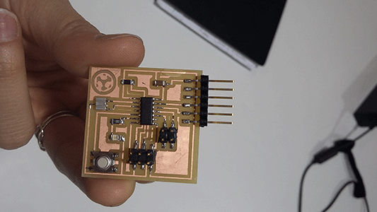
I also had some problems with the fabmodules because I gave 10mpx to the exterior traces because I considered it was going to be enough but the fabmodules didn’t recognize it as a trace so I had to modify the file again in Photoshop in order to 10mpx more so now my exterior trace had 20mpx. I imported it to fabmodules and it worked!
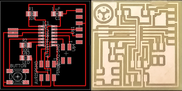
I milled it and the I soldered all the components.
FILES: