I want it to have several buttons so that I can control a motor left and right and also send a "enter" command to it for features like "stop" or "continue".
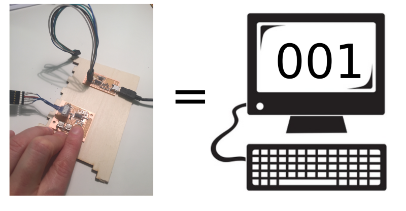
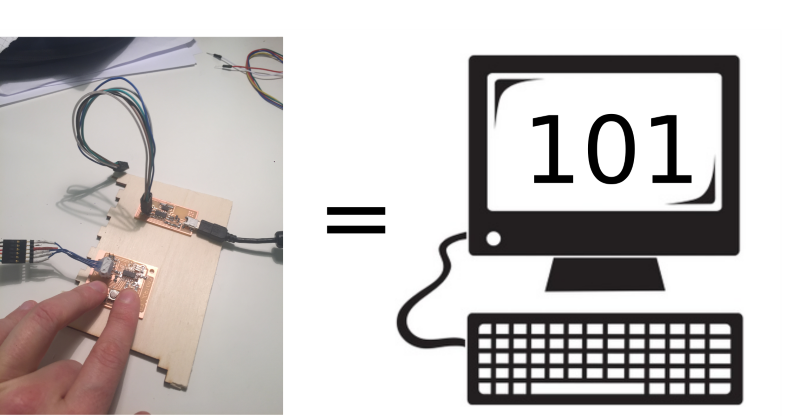
Result
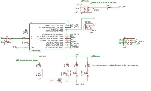
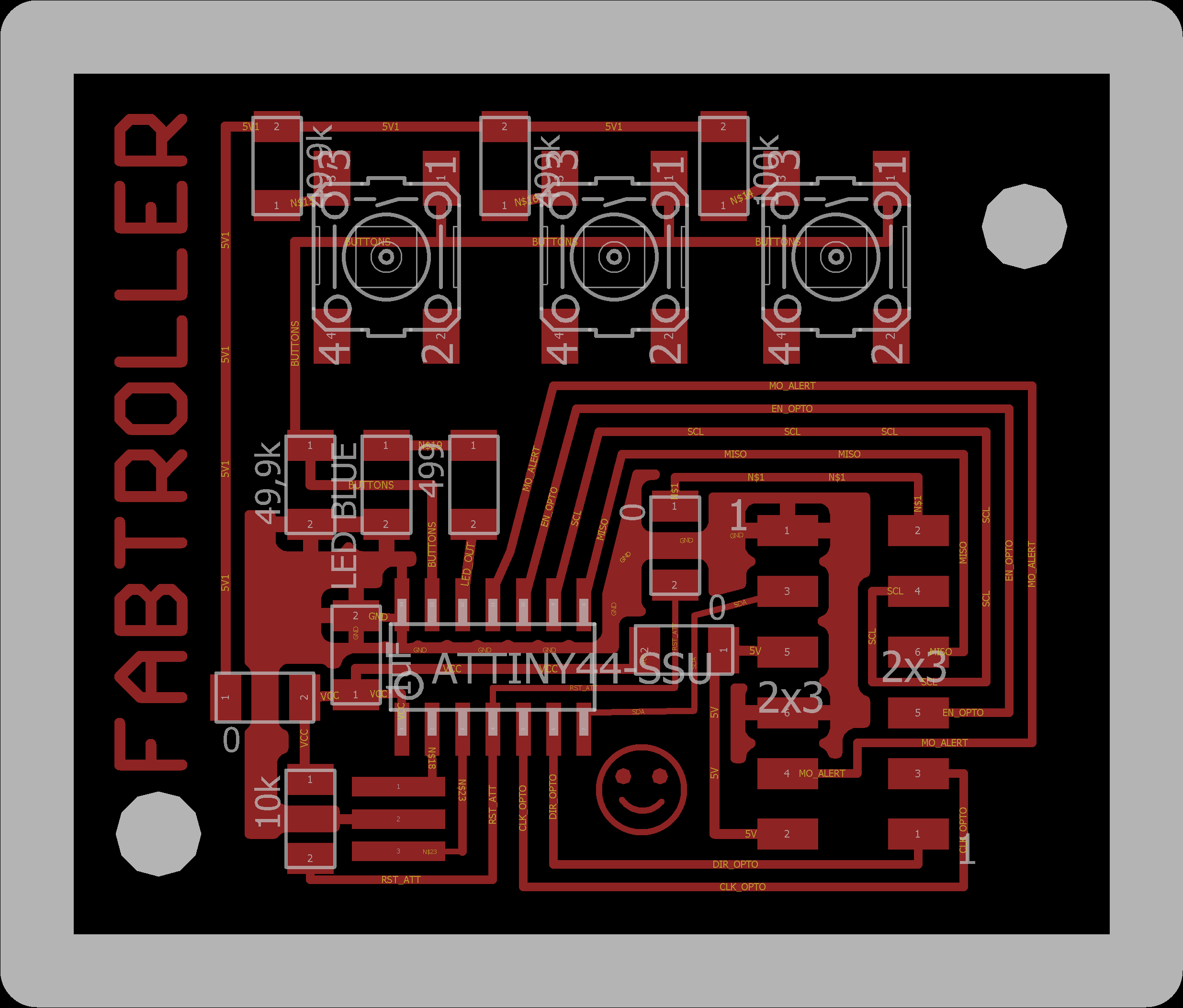
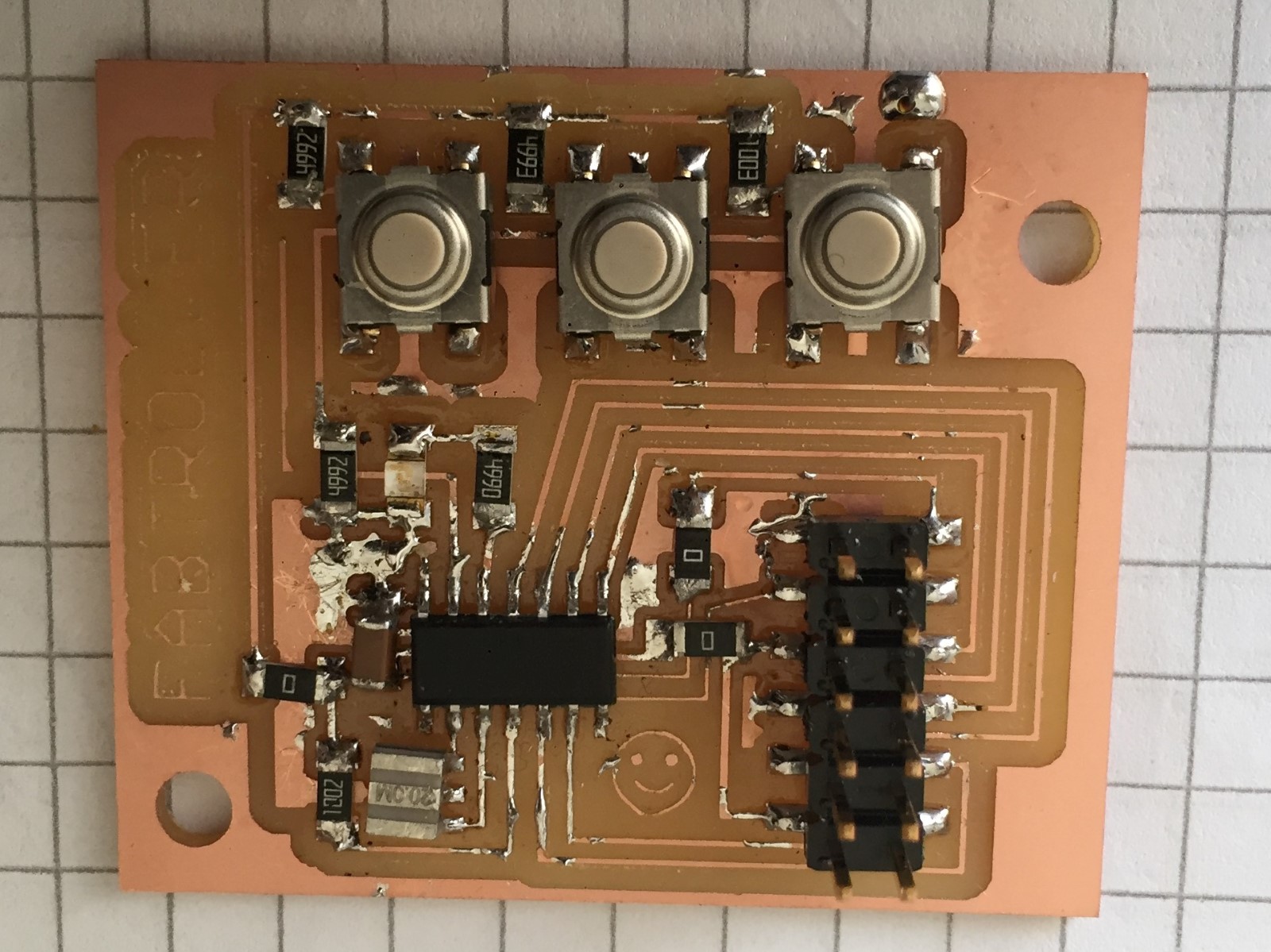
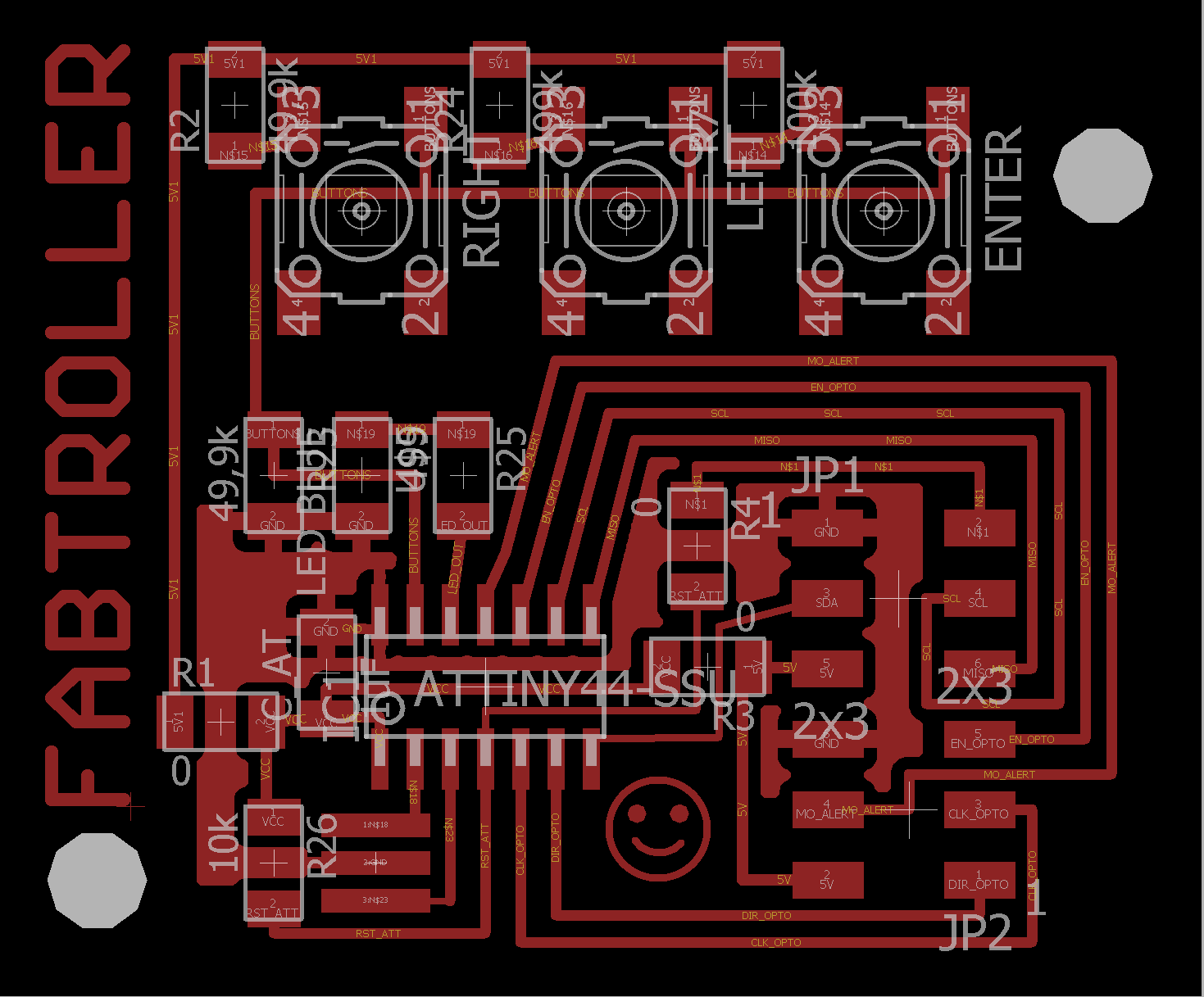
Features
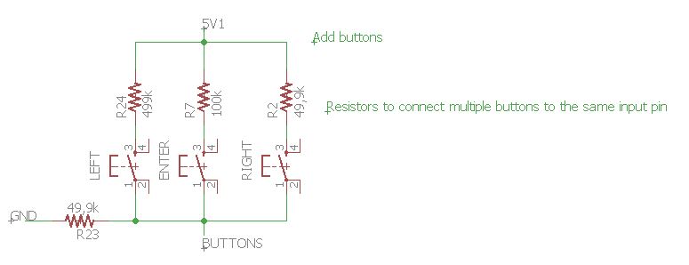
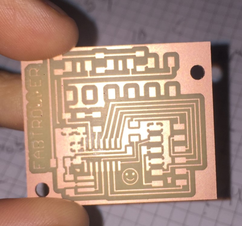
3 buttons = 8 possible button combinations, using one analog pin on the attiny44A microcontroller.
LED for user feedback
ISP header also used for serial comminication via FTID adapter
Stepper communication via separate 2x3 header
Video:
Arduino style program: The microcontroller reads the voltage, compares it to a list of voltages and prints the corresponding button combination to serial. I recieve the serial communication via Termite.
UPDATE!:
I ended up using this card to test and drive my final project CNC machine.
Here is a video of me controlling the the machine on Iceland in FabLab Isafjordur. The card is a bit hard to see but look in the lower left corner at 0:14.
Code: C code and makefile.(Not awesome, works with 20Mhz resonator) Arduino code (works fine with 8Mhz internal clock, disconnect the reset pin to use in with the arduino serial monitor)
Generating toolpaths for milling PCBs, my methods:
Guide Exporting good image from eagle for milling using mods for CAM.
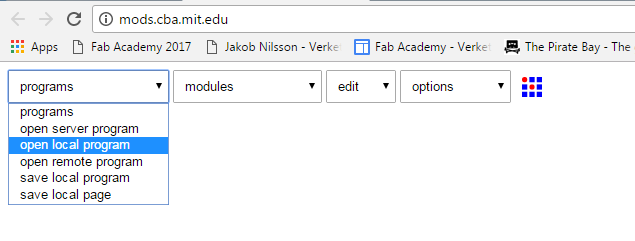
Guide Using Mods for Mach3 milling. Now with instructions!
Guide Exporting G-code from EAGLE using PCB-Gcode (My recommendation)
Multiple buttons on one pin
It reads which buttons that are pressed and sends the information to the computer, like this:
How does it do that?
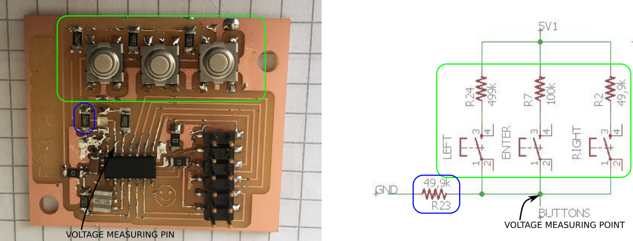
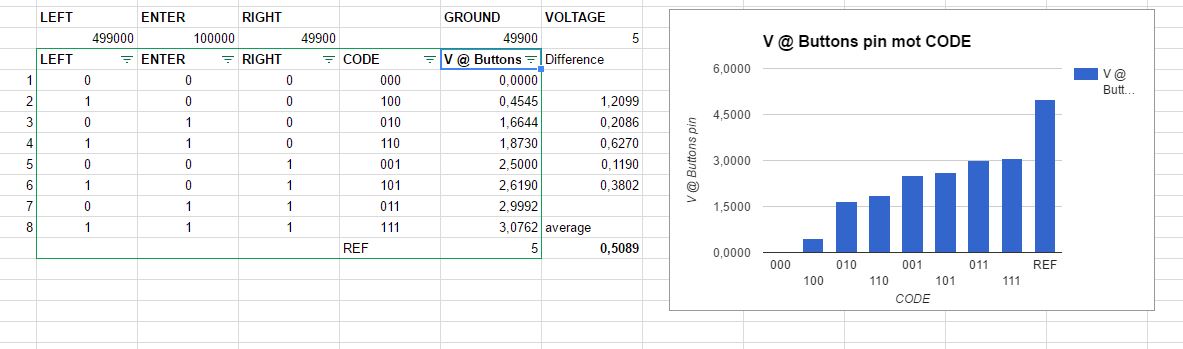
All the buttons are connected to the same input pin on the microcontroller. Every button has a different resistor connected to it, so when any combination of buttons is pressed it will create a unique voltage level at the input pin. Like this:
I then compare the measured votlage to a list of the expected voltages to find out which button combination is being pressed.
Status
I have made this controller card and a stepper driver card for week10 my next step will be to use them together which will be a good step on the way towards my final project where I will need to control four stepper motors and drivers. I am glad that I choose to do something that relates to my final project because I am quite impressed with how long everything takes to do!
Problems and challanges
Writing in C takes an enormous amout of time, I spent the entire friday on getting the microcontroller to read the buttons and send the result over serial. I like that you get close to the hardware and see what actually is going on but it just it too slow for me to get anything practial done.
For some reason I could not get the arduino library SoftwareSerial to work while using the external resonator component. When I set the fuses to use the internal 8Mhz clock it worked fine.
In week10 -ouput devices I made a stepper driver for my final project, a DIY CNC. Now I want to make a controller card with buttons, alert detection, led feedback and communication headers to interact with said stepper card. After initially trying to fit all this on it on the stepper driver card itself I decided to instead divide it into two separate cards.
Multiple buttons on one pin for using Analog voltage reading
I mentioned wanting buttons to interact with. I figured three is a good starting point, then I can intuitively drive the motor in both directions and give it commands, like move faster, by pressing the middle button at the same time. However, the number of pins are limited and it feels wasteful to occupy three pins for this purpose, so I looked into connection multiple buttons to one pin and using resistors to create a different voltage level for each combinaiton of button presses.
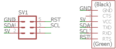
I wanted to be able to have my controller card talk to my PC. My first though was to add a straight 6 pin FTDI header so I could attach a USB-to-Serial cable directly to the controller card. After struggling with different PCB designs where I had both FTDI headers and ISP headers on the same card I decided to just reuse the programming header since I would not be programming the microcontroller at the same time as talking to the PC.
These are the pins I reused. The ISP header is on the left and the FTDI header is on the right.
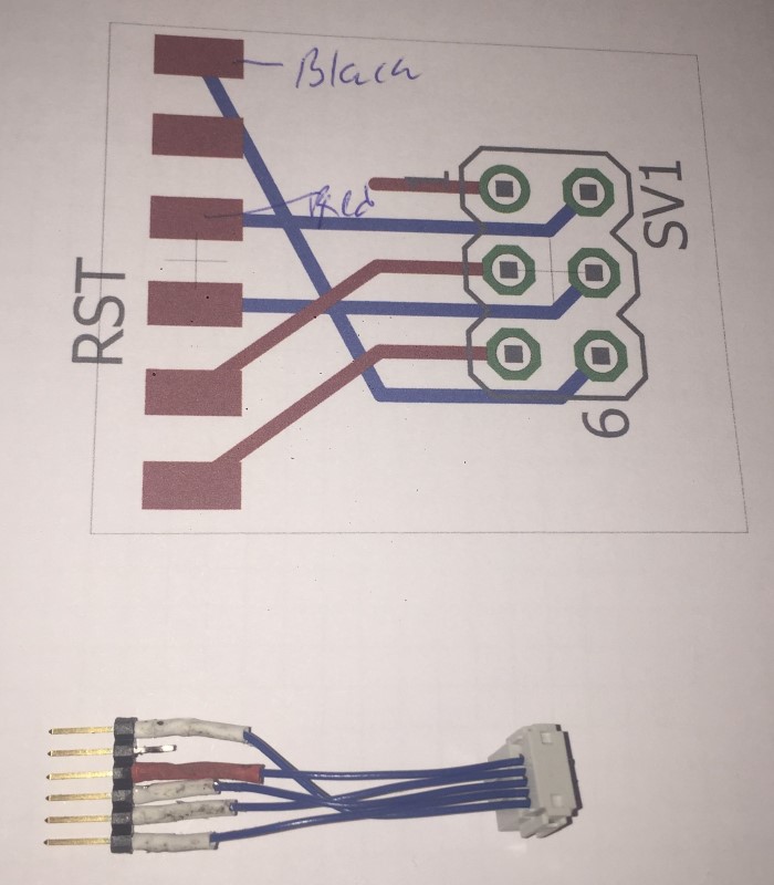
I made a "board" in eagle just to make it clear to myself which cable goes where. The finised adapter is shown on the bottom. Note the red sleewe to avoid connecting it the wrong way.
Schematic and cut files from Eagle to Mods
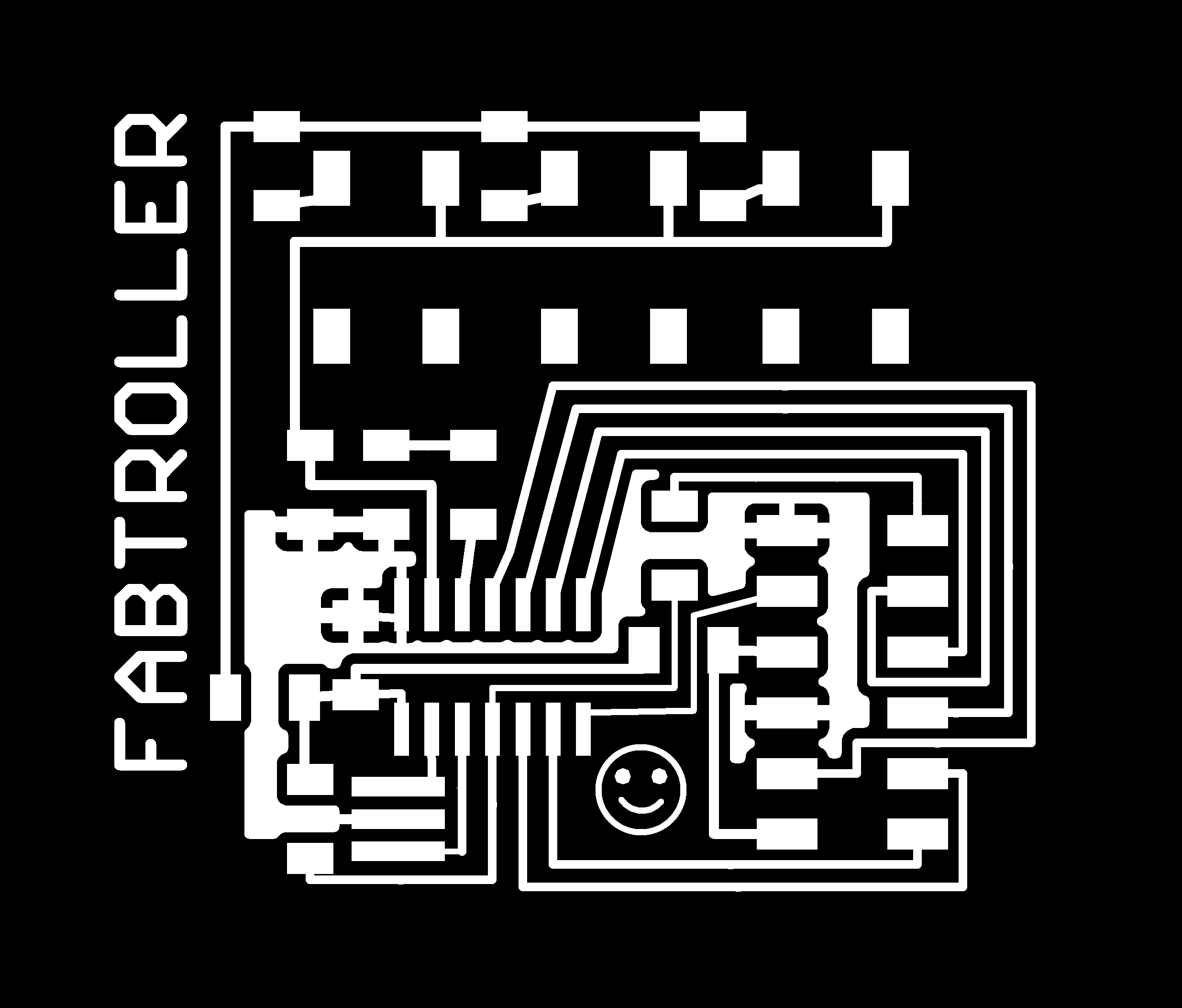
To generate good black and white files for Ø0,4 mm bit trace milling and Ø3 mm bit cutting in mods from EAGLE use this workflow:
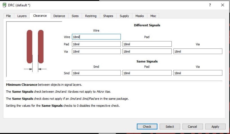
Check that you have 18 mil clearance everywhere, use the Design Rules Checker (DRC) under Tools->DRC. It should look like this, then press Check
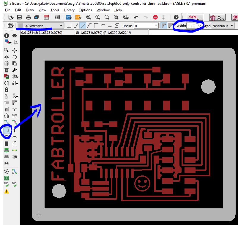
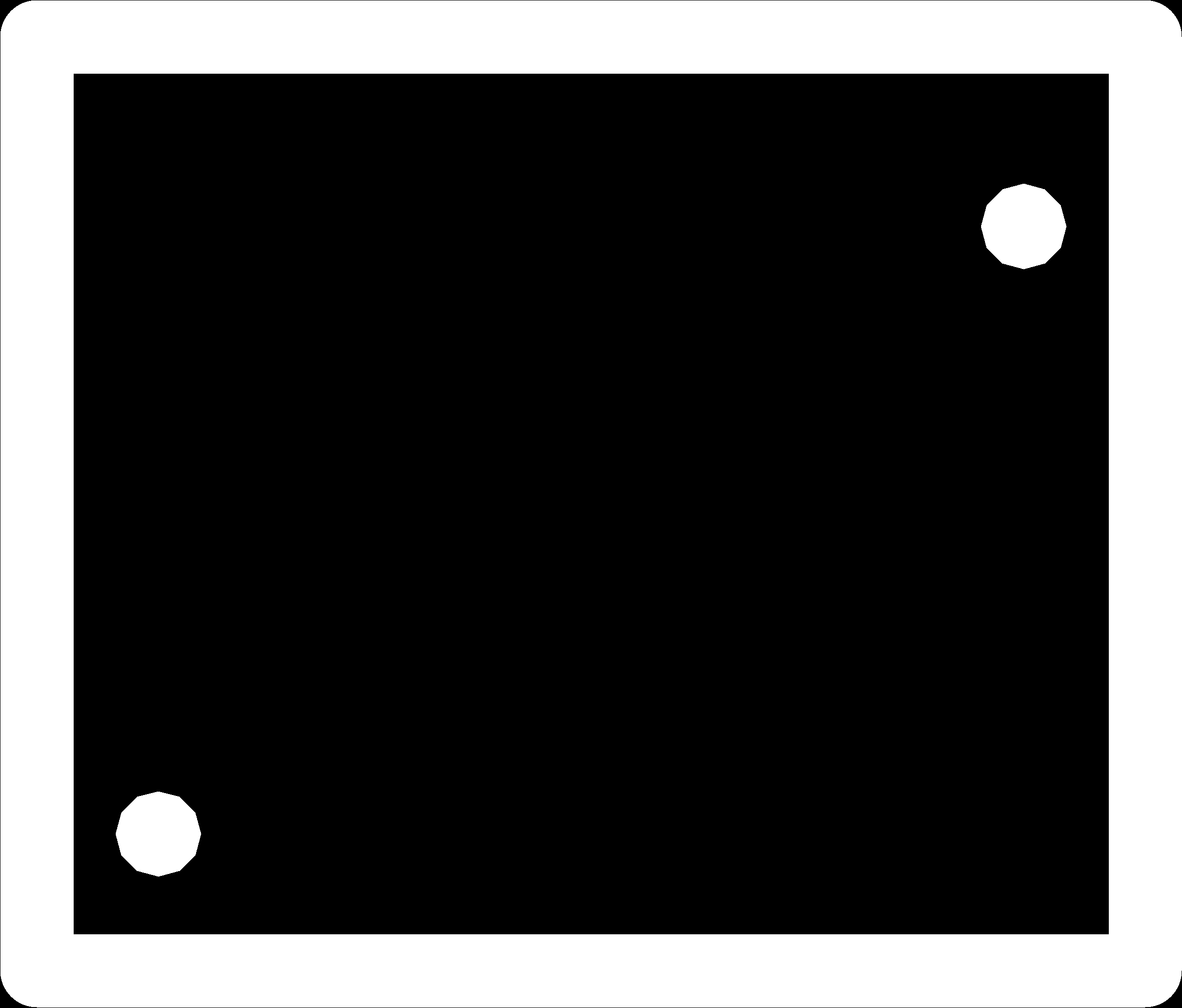
Draw a border using the Line tool with width set to 0.12mil (3.05mm) and draw it in the Dimension layer as in the picture below.
The line needs to be slightly wider than your milling bit for mods to understand what to do.
UPDATE! If you after doing the above also fill in the entire middle area with a rectangle drawn on the Dimension layer your milling paths will be even better.
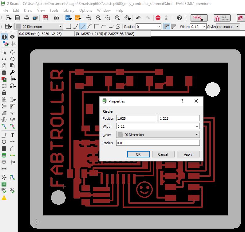
If you want mounting holes, draw them as cicles and set a tiny radius and the same line thickness as the border. Like this. Increase the Width value to get larger holes.
The hole needs to be slightly bigger than the bit so that mods understands what to do.
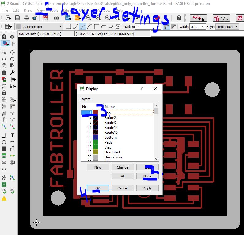
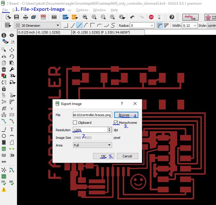
Turn on one layer and export it as a monochrome (black and white) picture
Make sure you draw the border before exporting, or your pictures will have different sizes.
This is how you turn on the top layer only:
This is how you export your traces as a black and white picture:
The DPI setting is important for mods to work well. You should only be seeing your copper traces when you do this step. Like below:
Now repeat the process but for the Dimension layer instead of top. (Dimension should only contain the area of the card you want cut.)
Note:
The cut out milling might with mods might give you some wierd extra outside of the card milling paths. This is a bug I know of but does not ruin the card and does not take long.
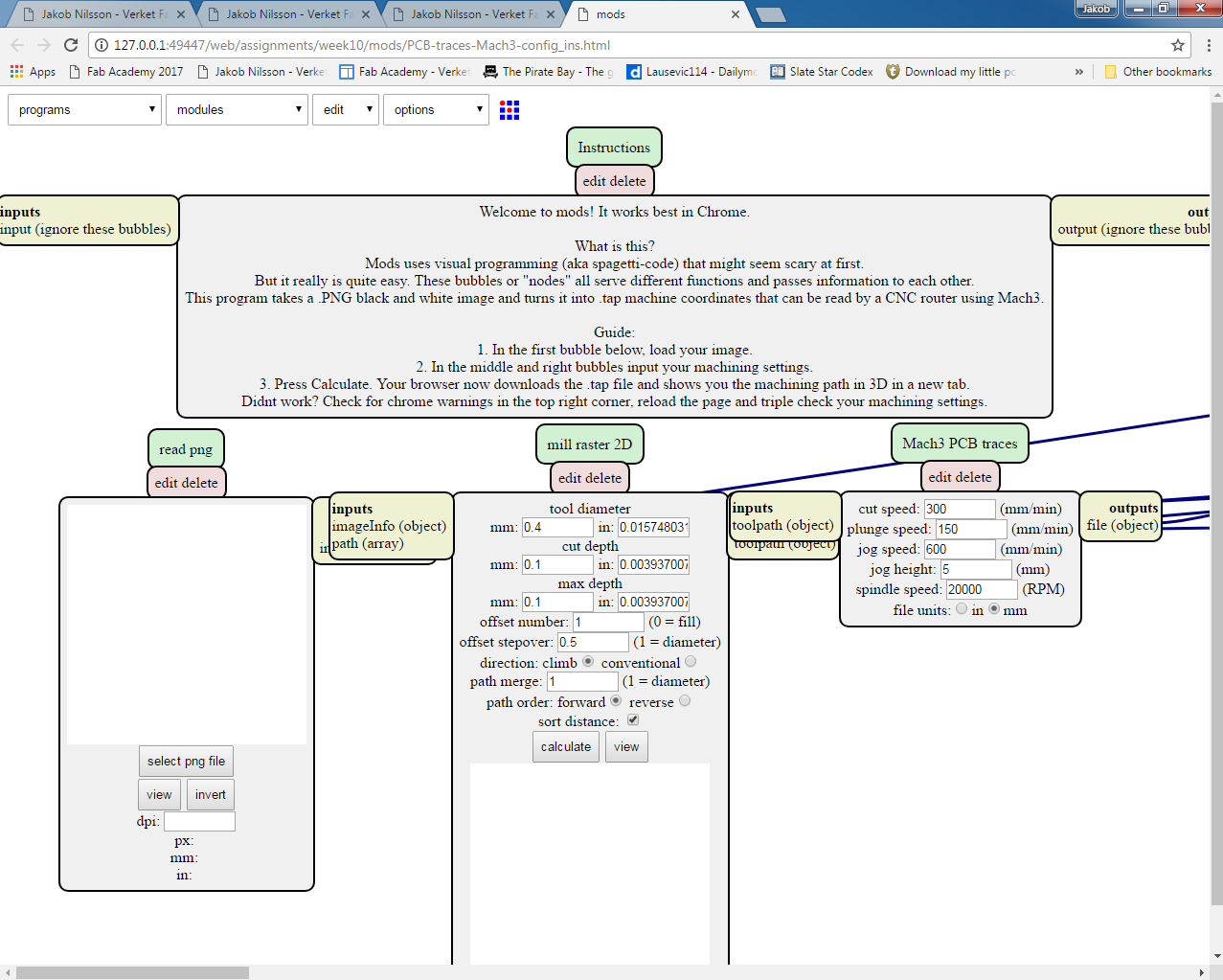
You will now see my instrucitons on the top of the program page, here is a preview.
It reads .PNG files, like the ones above. The resolution should be 1269 DPI or you will have problems.
It needs 18mil (0.4572 mm ) clearance for a Ø0.4mm bit to pass between your traces. 0.12mil (3.05mm) works for Ø3 mm cutout bits. Anything less than that might give errors that are hard to spot.
Load the file you want to mill by clicking select png file
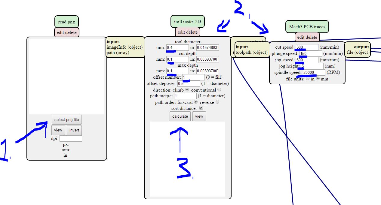
Adjust settings if needed, see the ones I underlined in the picture below. Most important is to use the correct tool diameter.
Press calculate when you are done, this will automatically save a .tap file in your downloads folder and open a tab showing you the milling paths in 3D.
To cut out the card. Load an image into mods with the areas to cut and invert it if needed (use the invert button), remember to set milling bit diameter, max depth (thickness of your card) and cut depth (for each pass).
Troubleshooting:
The .tap file does not download: Check chrome for warnings in the top right corner. It might suddenly start blocking them.
No new tab opens when I press calculate: Check chrome for warnings in the top right corner. It might suddenly start blocking them.
Same problem as above, but no warnings from chrome. Try reloading the page. This means you have to re-enter the settings.
Same problem as above, reloading doesn't help. Your settings might be wrong, check if you have mixed up Cut depth and Max depth.
The cut out milling gives you some wierd extra outside of the card milling paths. This is a bug I know of but does not ruin the card and does not take long. I think it has something to do with how the image is inverted. UPDATE! A good workaround, in EAGLE, for this is to fill the entire area inside the dimension lines with a rectangle in the same layer (Dimension) then it will not generate the extra passes.
Input data in this sequence:
Background and reference
I heard that Instructor Jens had successfully made a mods program to generate G-code for his DIY CNC. REPO This made me try to do the same for the Mach3 .tap files that we use to run our CNC router to mill PCBs here at Verket Fab Lab.
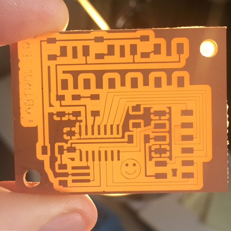
I used my own mods-mod to mill the card with the SaleCNC router using Mach3 software. Worked fine! For the traces I used the setting shown in the picture above and they are also default in the program.
For the cut-out and hole I used a Ø3mm milling bit and 1200 mm/min cutting speed, 0.6 mm cutting depth per pass and 1.55 total cut depth (to save the vaccum table top). Also worked fine!
My first attempt turned out to be to optimistic (at least using the vaccum table). Traces with widths lower than 0.007inch (0.18 mm) didn't survive and the ones that did (all critical ones actually did) looked like they would break if scratched. So I decided to beef them up a bit.
Here I have used twice as thick traces 0.014 inch (0.3556 mm) as a base case and only gone lower where space didn't allow it.
On both cards above I used a local "ground plane" to beef up the traces used for grounding the different components together. This is done to minimize the risk of ground not being an equal reference everywhere.
I have connected my buttons to PIN 13, • Port A, Bit 0 – ADC0/AREF/PCINT0 • ADC0: Analog to Digital Converter, Channel 0.
To do this I refer to chapter 16 in the data sheet.
16. Analog to Digital Converter
"In order to be able to use the ADC the Power Reduction bit, PRADC, in the Power Reduction
Register must be disabled. This is done by clearing the PRADC bit. See “PRR – Power Reduction
Register” on page 37 for more details." Comment: Seems to be cleared as default. Action: None.
"The ADC is enabled by setting the ADC Enable bit, ADEN in ADCSRA. Voltage reference and
input channel selections will not go into effect until ADEN is set. The ADC does not consume
power when ADEN is cleared, so it is recommended to switch off the ADC before entering power
saving sleep modes."
Comment: OK, so we need to enable it. Action: Add this code:
ADCSRA = (1 << ADEN) | // Enable ADC
"The ADC converts an analog input voltage to a 10-bit digital value using successive approximation.
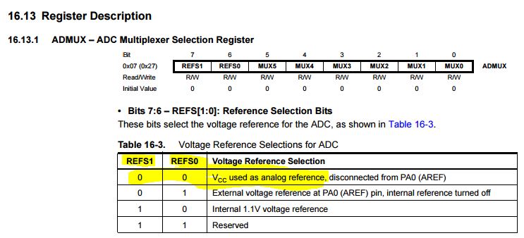
The minimum value represents GND and the maximum value represents the reference voltage. The ADC voltage reference is selected by writing the REFS[1:0] bits in the ADMUX register.
Alternatives are the VCC supply pin, the AREF pin and the internal 1.1V voltage reference."
Comment:" We want to use VCC as reference. Action: Look up how to do that under this headline:
So we add this code:
ADMUX = (0 << REFS1) // Sets ref. voltage to VCC, bit 1
ADMUX = (0 << REFS0) | // Sets ref. voltage to VCC, bit 0
NOTE!: They all have initial value 0 so this is actually not needed!
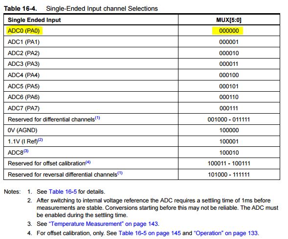
We read on in chapter 16: "The analog input channel and differential gain are selected by writing to the MUX bits in
ADMUX. Any of the ADC input pins can be selected as single ended inputs to the ADC. "
"• Bits 5:0 – MUX[5:0]: Analog Channel and Gain Selection Bits
The value of these bits selects which combination of analog inputs are connected to the ADC."
Comment: So we need to set all 6 MUX bits to 0 (0 to 5 = 6).
NOTE!: They all have initial value 0 so this is actually not needed!
We read further in chapter 16:
"The ADC generates a 10-bit result which is presented in the ADC Data Registers, ADCH and
ADCL. By default, the result is presented right adjusted, but can optionally be presented left
adjusted by setting the ADLAR bit in ADCSRB.
If the result is left adjusted and no more than 8-bit precision is required, it is sufficient to read
ADCH, only. Otherwise, ADCL must be read first, then ADCH, to ensure that the content of the
data registers belongs to the same conversion."
Comment: Dealing with two registers sounds complicated, 8 bit precison should be enough for me since my minimum difference between signals is 0,12V and 8 bit=256 steps per 0 to 5 V gives us = 0,02 V per step, resulting in 6 steps between the tightest signals. Actions: Use the simpler left adjusted 8 bit conversion, by "by setting the ADLAR bit in ADCSRB." Done with this code:
ADCSRB = (1 << ADLAR) // Set to 1 on to choose the 8 bit (lower) resolution mode instead of 10 bit.
We read further in chapter 16:
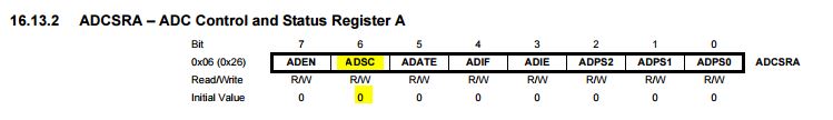
16.4 Starting a Conversion
"A single conversion is started by writing a logical one to the ADC Start Conversion bit, ADSC.
This bit stays high as long as the conversion is in progress and will be cleared by hardware
when the conversion is completed. "
Comment: Sounds good, let's do that. Action: Add this code:
ADCSRA = ( 1 << ADSC ) // Make one analog to digital conversion, start now.
NOTE: I have ignored the prescaler since I make single samplings. I am not sure how it would work.
"ADSC will read as one as long as a conversion is in progress. When the conversion is complete,
it returns to zero."
Comment: So we wait for it to finish and then read the result. Action: Add this code:
while (ADCSRA & (1 << ADSC)) // wait for AD conversion to complete by checking if the ADSC bit is still 1 in ADCSRA
;
//This is an intentially empty loop, it just holds until it is done converting.
//
// send result
//
chr = ADCH; //Here is out result since we used the 8 bit resolution.
put_char( &serial_port, serial_pin_out, chr);
char_delay(); //To not spam to quickly. Possibly not needed.
after on day of C this is the Result, I can get it to send stuff over serial that changes with button presses but I can't decode it on the other end. Straight C is turning out to be harder to work in than expected and I feel it will take to long to get anywhere practical in the time available. I rather switch to the arduino IDE where I know I can make things work faster.
Tried arduino, got it working (with the led) in 5 minute, will contiune there. Serial seems to be covered on forums.
Got SoftwareSerial working by setting the fuses to use the internal 8 Mhz clock, which I didn't have to calibrate. I could not get it working with the exernal 20Mhz resonator. I used the same highlowtech.org tutorial as in week8
 pinout