The issue is resolved, this new example file has been added to the tutorial. You should use it instead if my version
I asked in the Ohad-group-chat and user Cept told me to use Tapans files, apparently he was a 2016 student who kept his files on this google drive.
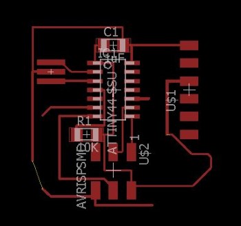
This is Tapans board (left) next to the original Hello board (right). Apparently he has already made his personal modifications to it.
Recreating the example files
Removing the extra components
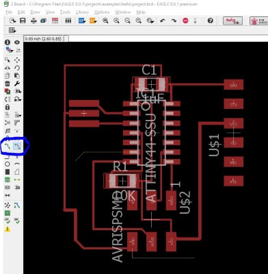
To indicate where I use an eagle command it have put it's name in quotes like "this". The commands can be accessed in the icon menu on the left (roll over with the cursor for information about each), from the text-menues Edit, Draw and Tools or by typing it's name in the command bar on the top.
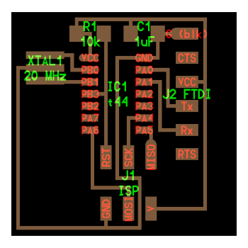
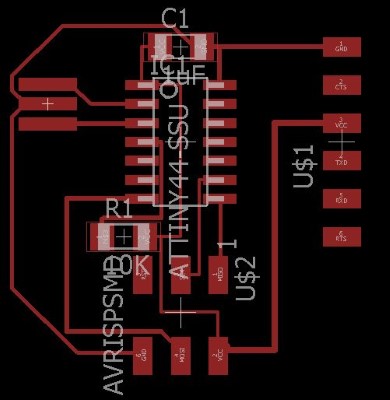
I decided to recreate the original Hello echo as a first exercise. I'll do that by "deleting" the extra components in the schematic and seeing what that does to the board layout.
Indeed, the components got removed.
Apparently I need to clean up the leftover traces. I used the "Route" and "Ripup" commands modify the traces. Some loose ends remain. My bord on the left. Reference to the right.
I used the "Identify" and "Show" commands to give me the names and highlight what in the schematic was causing the loose ends on the board.
I used Ripup to remove ugly traces and replaced them with autorouted traces, I didn't mess with the autorouting settings yet.
Restoring the layout
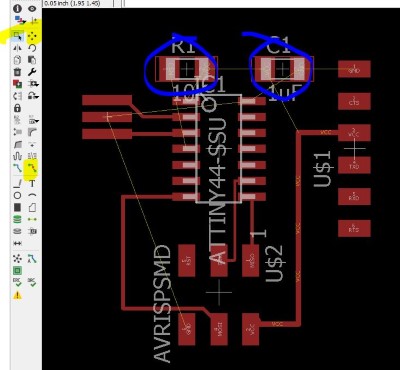
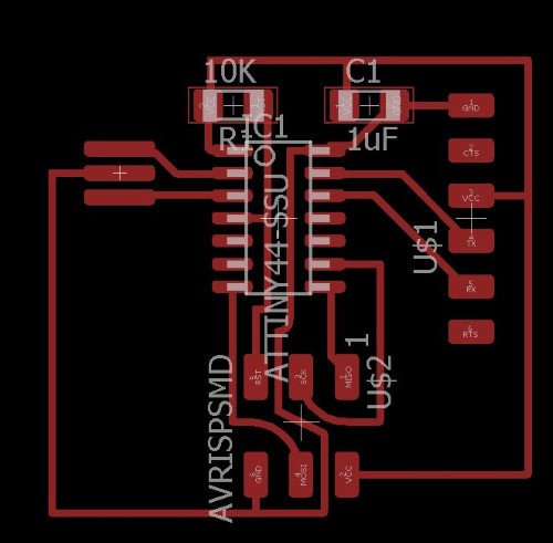
Now I wanted to see if I could remodel it to the original layout. I moved up the resistor and the capacitor and ripped their connection (left). I let the autorouter add them back (right).
Starting to look like the original (shown on the right)!
Debugging the circuit
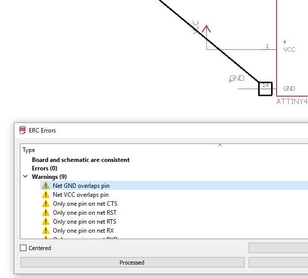
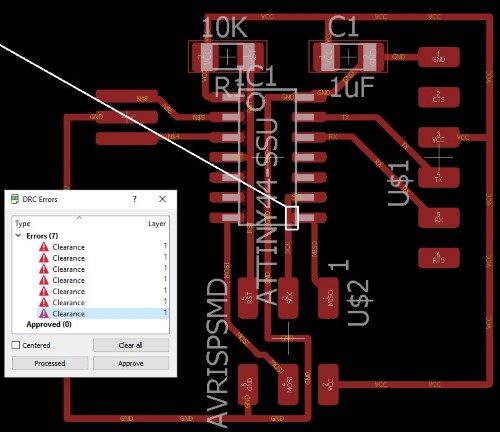
To verify that your circuit does not cointain errors or mistakes it is prudent to run the Electrical rules checker "ERC". You will find it under Tools-ERC or as it's own button on the side.
Below is the resulting errors list. The overlap-error happens when a "net" is on top of a component but not connected. This can happen if you use the "line" tool to draw the connections instead of the "net" tool. I fixed the VCC and GND errors by redrawing the nets for them ("delete" then "net" as before.)
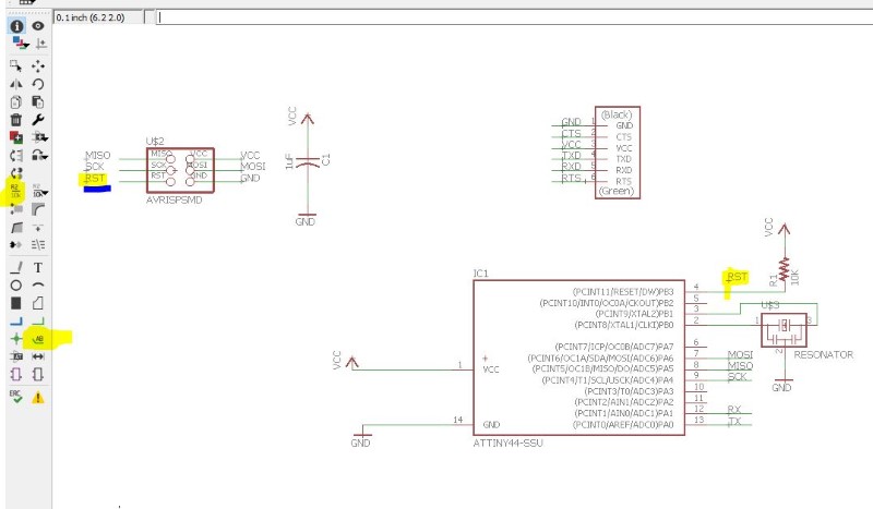
The "Only one pin on net RST" is actually an error in Talpans schematic, the RST pin on the header should be connected to the pull-up resistor, as shown in the reference picture below on the right.
I also see several short cricuits between the IC pins and pads touching the traces, I'll have to redraw those traces.
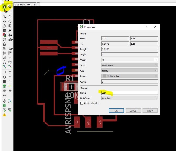
I recreated the missing RST connection by adding and linking "Label"s to the net. (I put it in the same place as show in the tutorial reference schematic.) You link two (or more) lables together by using the "Name" command to rename them to the same name, in this case "RST". Then you get a question if you want to link them. Note that just pressing "Info" and renaming the label does not work, then you get an error message instead.
This added the missing link in the board layout. Yay!
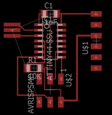
I added the remaining missing connections using the same workflow:
Add a piece of "net", give it a "label" and "name" it to link it to another label.
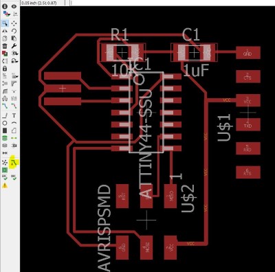
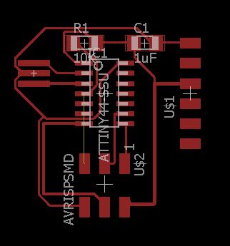
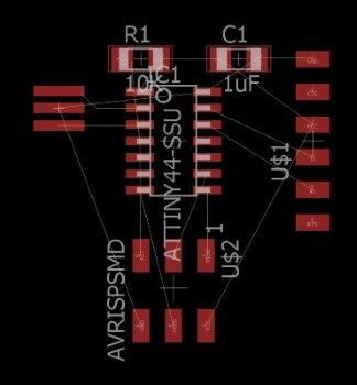
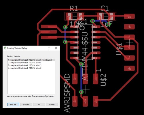
When I had no unadressed errors in the ECR for the schematic list I switched to board layout. I decided to start over and completely reroute it. To do this I clicked "Ripup" and then "GO" to ripup all signal traces completely.
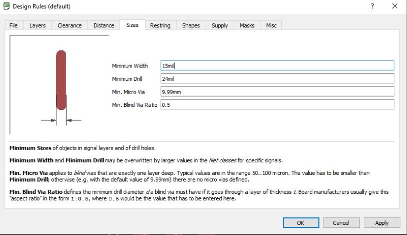
Design Rules Checker (DRC) Settings for milling
I setup the Design rules to work with outØ0,4mm milling bit. Meaning that all gaps must be at least 0,4 mm or 15mil (15/1000 inch). I measured the trace width used in the FabISP to ca 15mil as well so I used that for both. I also added 8mil (0,2mm) radiuses to all pads to test it.
Routing the board
Autorouter could not solve the routing witout "jumps" or vias so I decided to give it some help and lay a groundwork.
Apparently "mirror" does something else than just flipping the component over. "Rotate" works better. I liked the routing! It was fun and it feeled like gamefication with rewarding sounds when you did something right. I routed most of the board manually and the then used autorouting for the obvious ones. The DRC check informed me that the middle got to tight.
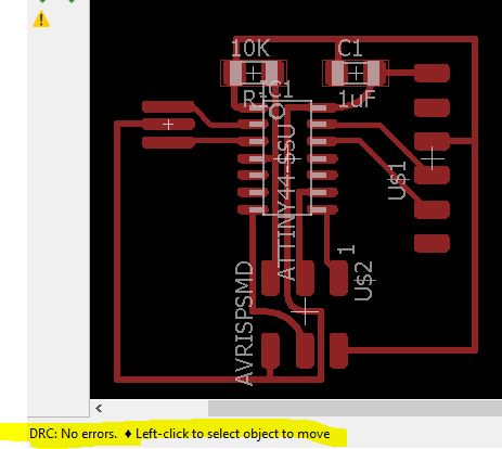
I managed to get it though the check by re routing one of the wires going through the middle.
But I knew it should be possible to do it through the middle as well so I reduced the grid snap so that I could fine tune them.
That solved the problem and I could complete the restoration of the original example file.
Recreated Hello echo files for eagle
I sent out a message to my group that they could find restored example files here.
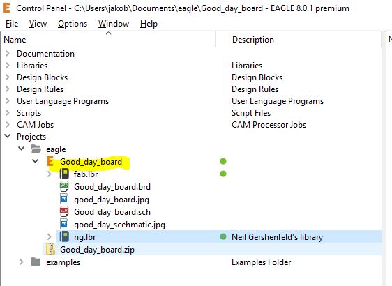
I have successfully recreated the hello echo-world board we were supposed to start with. I packed all the eagle files and libraries in this zip file. To use them in windows, just unzip into your windows Documents/eagle folder. Then it should appear like this:
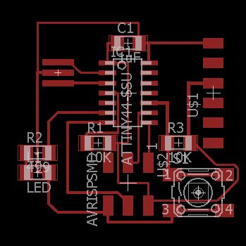
Adding the LED and button
Copied my Good_day_board to a new folder and renamed it.
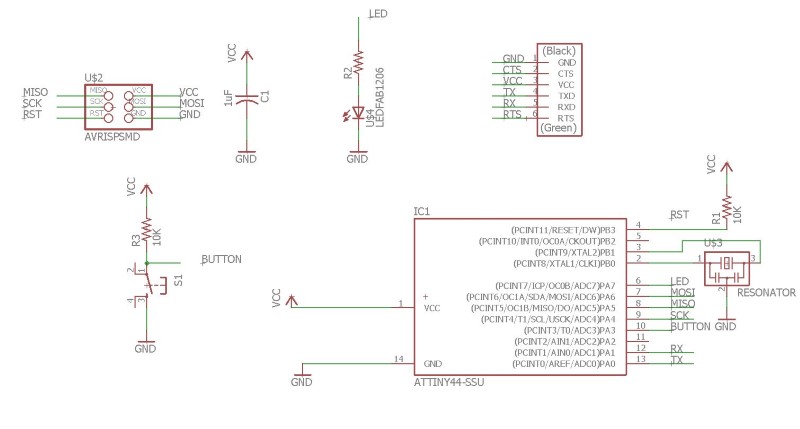
Added the components from the fab library, (used the versions with the -fab sufflix) the button is called a OMERON switch. I'll use a 499ohm resistor since I know we have it in stock and that it will work according to the tutorial.
I looked into different ways of lighting the LED directly when the button is pressed but didn't find a design that I liked but it will be easy enough to do in software. I also contemplated if I could share the pull up resitor used for the RESET pin with the button, but soon realiced that it would trigger a RESET if you then pressed the button. So I stuck to the basic circuit for now.
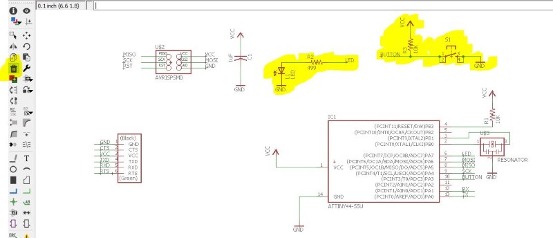
Connecting new components to the circuit
To connect two points in the circuit layout without using a net between them in you do this: (commands/buttons "in quotes")
Add a short bit of "Net" to the connection points you want to connect (or it will not work).
Add a "Label" to both pieces of net (it will get an automatic name)
Use "Name" to rename both to the same thing, you need to select the little + sign, it can be hard to hit.
You will then get a question if you want to link the points. Answer yes :)
You can also rename things using the "Info" command, but you can not link things this way.
Check and route the circuit
After running the ERC test (had forgotten to add the reistance value) it was time to route the new components.
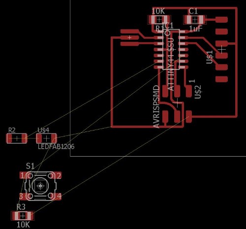
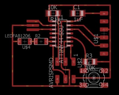
I Routed them manually (shown on the left)! But since I used the original layout of the hello echo board it came out looking very much like the tutorial version. I wanted it to be at little more personal so I moved some components around so that I got the LED in the corner and made the board a bit more narrow. (Result shown on the right.) I like to do the routing, its easy to just want to do it a little bit more...
I ran the DRC check with the same clearance and width values and adjusted where I had too tight clearnaces unitl it was error free. It really helps with the fine tuning to have a low value for the alternative grid setting, i used 0,05 in for the main and 0,005 in for the alternative grid. (the alternative grid activates when you hold down ALT while you are moving things).
Fabrication of circuit boards
Exporting from Eagle to Fusion360
I'll be milling this on a SaleCNC using Mach3, like I did in week4.
I tried the Autodesk-make button in the top menu for exporting it. It let me send the board to their ecad.io page. From there I saved an assembly MCAD file with the traces as solid model features in the STEP format for importing it into fusion360 where I want to do the CAM.
Workflow
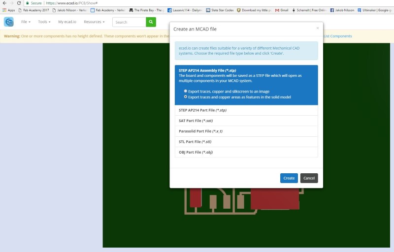
Press "MAKE" in the top Eagle menu
This opens a browser, press "My ecad.io"
Go to your file
Press the "Action" menu
Select "Create MCAD file"
Choose Assembly or part (Assembly has better feature naming but Part is less complex to work with.)
Select "Export traces and copper areas as features in the solid model"
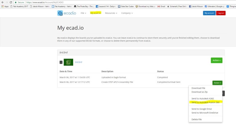
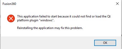
When the .stp file was done generating I used the option to send it directly to Fusion360.
Sadly that didn't work.
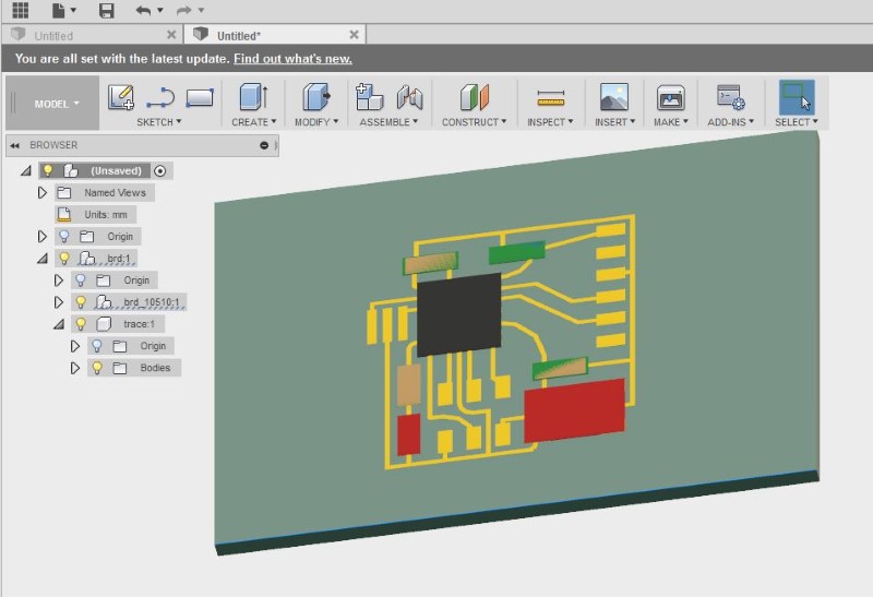
So I downloaded it and imported it manually.
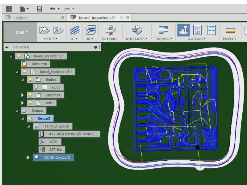
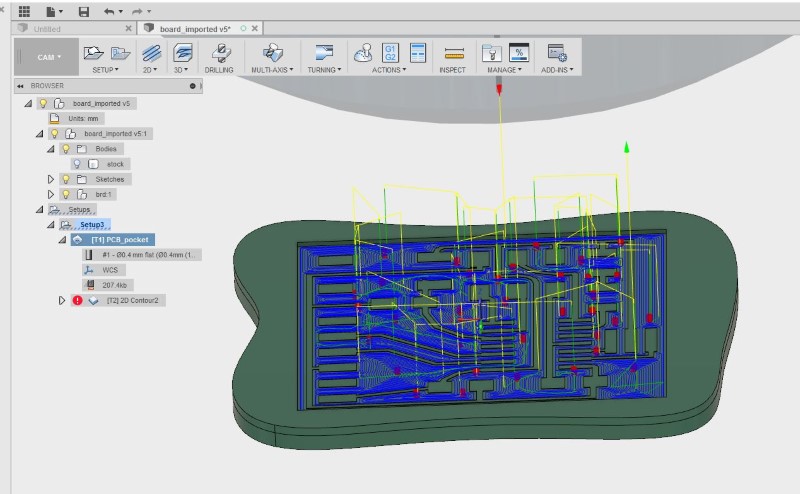
CAM in Fusion360
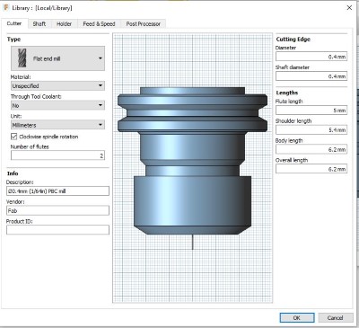
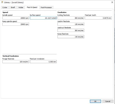
I setup a new milling tool with the same settings as I used in RhinoCAM during Week 4.
CAM HINTS!
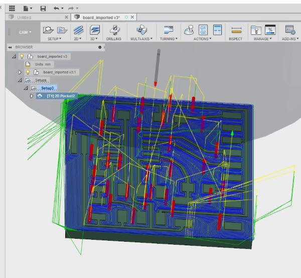
Use the 2D pocket operation to mill the copper around the traces.
You need to actually model a real pocket with a wall around the area to be milled, like this. Otherwise you will get the same error as I got.
Join the bodies for the traces to the PCB, otherwise fusion will ignore the trace.
Make extra sure that you Origo (zero position) is right on top of your board.
Adjust the thickness of the board so that your cut-out will not eat up your sacrificial layer
Use the built in mach3 post processor in Fusion360 to export the toolpaths.
Milling the board
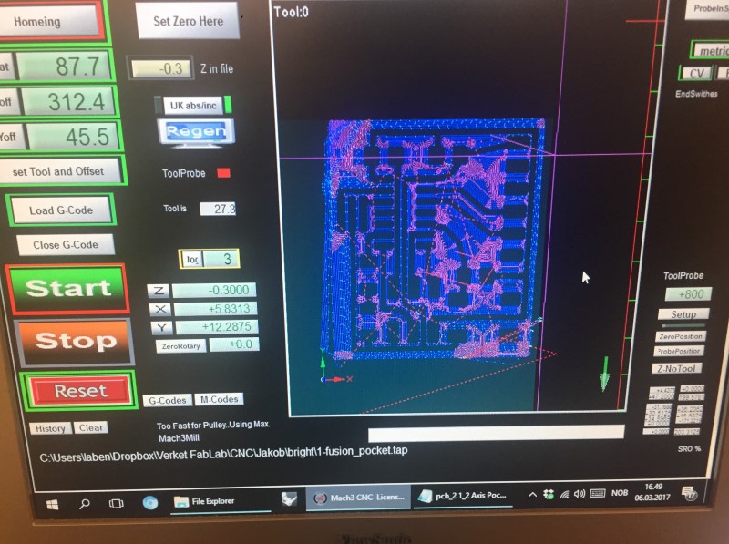
It imported fine to mach3 and I could set up the board and start milling.
I milled the card on the same machine and setup as in week4.
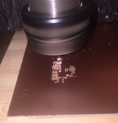
As it was being milled I saw that I had made an error in generating my milling paths in Fusion360, my pocket operation had several paths entering th PCB from the sides, causing ugly bit-stressing milling. I went back and checked this later.
I had a machine incident after changing the milling bit, the machine missed the z-limit switch with the tool and would have crashed the dust cover against it if I had not pressed the emergency stop. This was probably due to me not homeing after it was restarted. The solution was to restart Mach3.
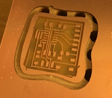
When I continued milling the next day my PCB blank had moved on the vaccum table so I decided to make a new larger cut out profile so that I would not risk damaging my traces when cutting it out
I re-zeroed the machine and cut out the card using my new profile.
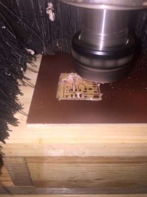
Fixing the milling errors
I investigated and found that I needed to create an actual pocket in my model for the CAM enigne to respect the sides. If it can't see it, it will think it is air. After remodeling the card it planned the path better.
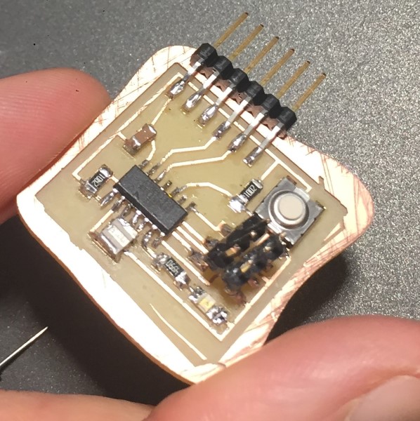
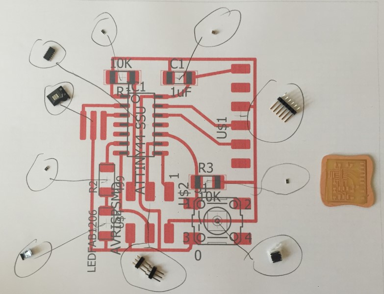
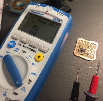
Time to solder! I first identified the components I would need.
Read up on LED polarity since it was hard to judge which side of the LED was Anode and which was Cathode and my multimeter would not tell me either.
Measuring the components in place
First I soldered all the passive components to be able to measure them in place. Everything seemed to work so I added the IC and measured further. However now the multimeter seemed to register that the LED was on backwards. I desoldered it using a soldering wick and remeasured. Turns out the IC was reading as a diode from ground to pin 6. That tricked me into thinking the LED was on backwards.
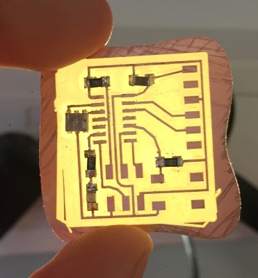
I added the LED back and added all the connectors. Complete!
Sadly we have no special FTDI-USB-TO-SERIAL cable in the lab yet, it is on its way so I can not yet verify that the serial communication works. I could program the board to do something else but I don't have the time to learn how this week.
Workflow to program a hello echo board using the FabISP in Windows10
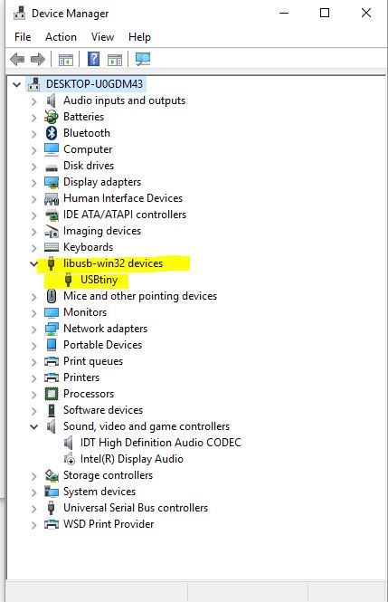
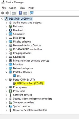
If you attach it to the PC with USB it should show up in your device manager like this
If it shows up like something else, then you need to download new drivers.
Detatch the USB from the PC when you have verified it. (To cut power before you connect your hello echo board.)
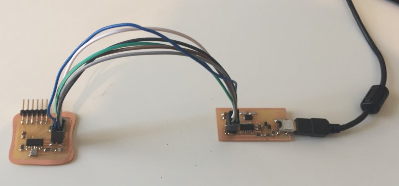
Connect your FabISP to your Hello Echo board same-pin-to-pin like this. (VCC to VCC etc.)
You need to have the 0-ohm jumper still soldered on to power the hello echo board from the FabISP.
Reattach the USB last.
If anything smokes or becomes hot, debug. Otherwise, congratulations on passing the smoke test!
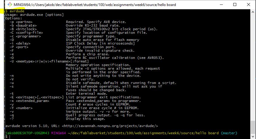
Make sure you have the AVRDude software installed by typing "avrdude" (without quotes in the command promt (to open press windows key, type "cmd", press enter) or in Bash. It should respond like this:
If it doesn't respond like that, you need to install it. You can follow my instructions steps 4-6 here.
Open a command shell (to open press windows key, type "cmd", press enter) or Bash and navigate to the folder.
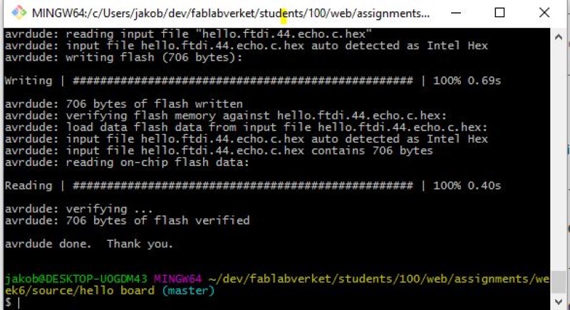
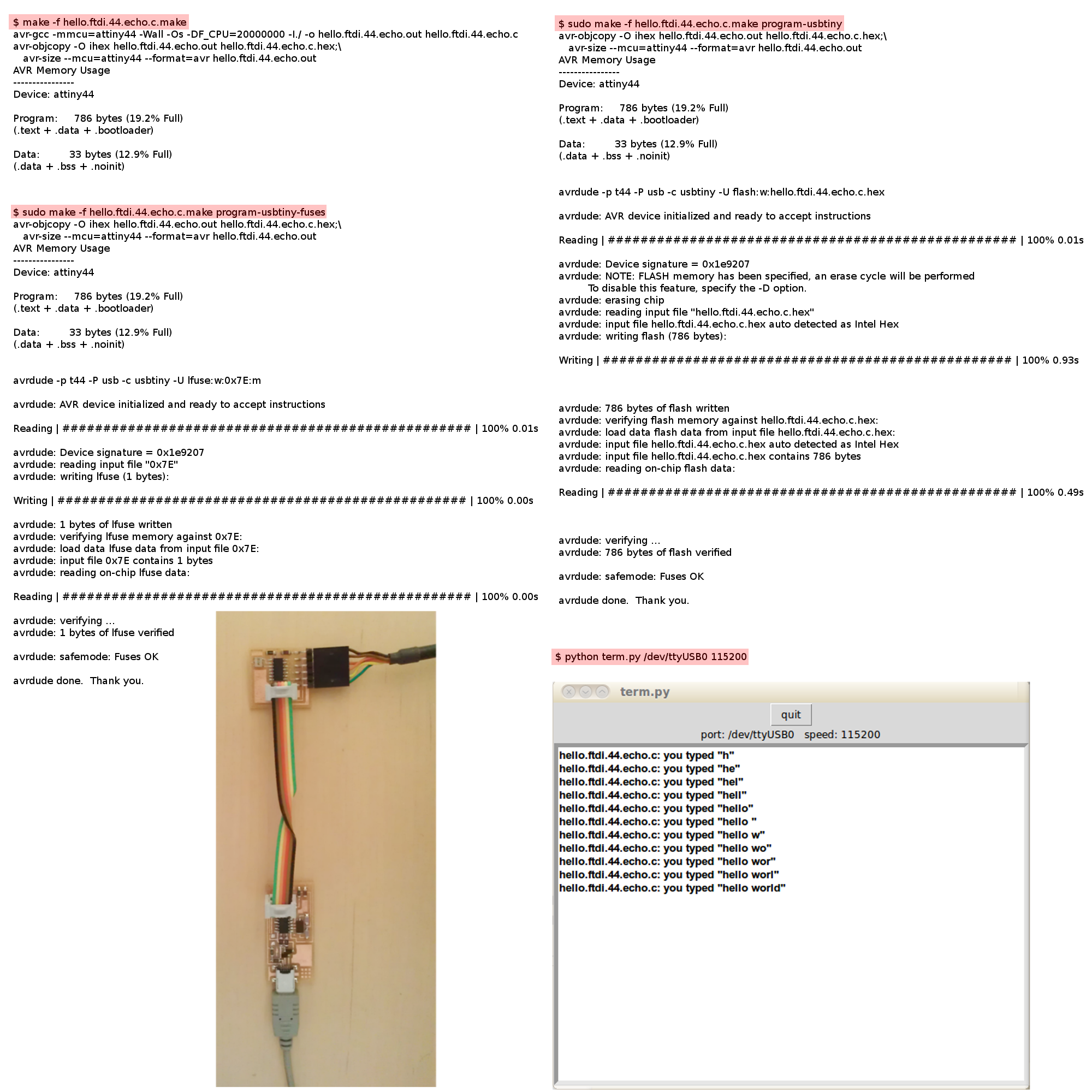
Then type and execute make -f hello.ftdi.44.echo.c.make
Type and execute make -f hello.ftdi.44.echo.c.make program-usbtiny-fuses
Type and execute make -f hello.ftdi.44.echo.c.make program-usbtiny
If you get errors, stop and fix them, they are probably due to some problem with your board.
That should end with this message:
Then you have succeded, congratulations!
UPDATE: Serial communication
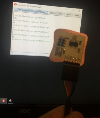
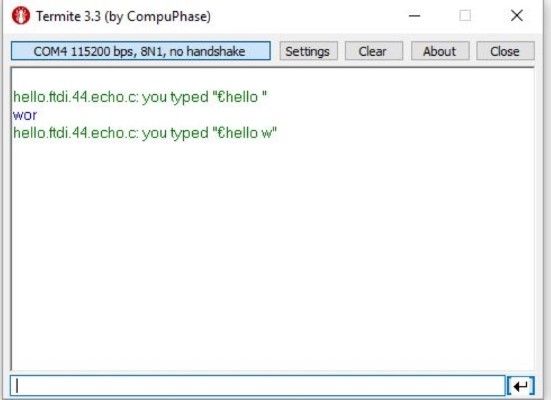
I found a FTDI cable in the lab, apparently we have them after all! After a failed attempt at using putty I tried Termite 3.3 which worked instantly.
I connected the card with the black cable going to the ground pin on the header.
I used the the windows device manager to find out which COM number the USB to serial converter occupied (for putty). I also set up its properties (Right Click->Properties) to be 115200 baud.
Termite found the right COM number without my help.
Success! This verifies my whole workflow from using the Arduino as a ISP, my FabISP and the Hello echo board I made last. Looking forward to making it do something with the button and diode.
.jpg)