Greetings, here lies my work-log at
______    _      ___                _                             _____  _____  __   ______
|  ___|  | |    / _ \              | |                           / __  \|  _  |/  | |___  /
| |_ __ _| |__ / /_\ \ ___ __ _  __| | ___ _ __ ___  _   _       `' / /'| |/' |`| |    / /
|  _/ _` | '_ \|  _  |/ __/ _` |/ _` |/ _ \ '_ ` _ \| | | |        / /  |  /| | | |   / /
| || (_| | |_) | | | | (_| (_| | (_| |  __/ | | | | | |_| |      ./ /___\ |_/ /_| |_./ /
\_| \__,_|_.__/\_| |_/\___\__,_|\__,_|\___|_| |_| |_|\__, |      \_____/ \___/ \___/\_/
                                                        |_|
electronics design
index
Assignment goals
- redraw the hello-world echo board to acquaint oneself with the process of designing circuits in softwares such as the ones listed below and completing the process of a prototyping a PCB, designing the PCB, milling it, stuffing it and finally debugging it
- KiCAD
- Autodesk Eagle
- DesignSpark
- MultiSIM
- Kokompe - soon to be added to mods.cba.mit.edu
- Add atleast a button and an LED to the redrawn board
- Stretch goals
- Get acquainted with diagnostic/electronic tools like the Oscilloscope and multimeter
- Simulate the PCB schematic
KiCAD v4 - Intro and resources
- Homepage
- Downloads
- KiCad roadmap for v5 and v6
- Official documentation
- Youtube page
I chose to learn KiCAD first as it is open-source and the learning documentaion resources seemed to be easy to follow . The documentation I followed - Getting Started with KiCAD
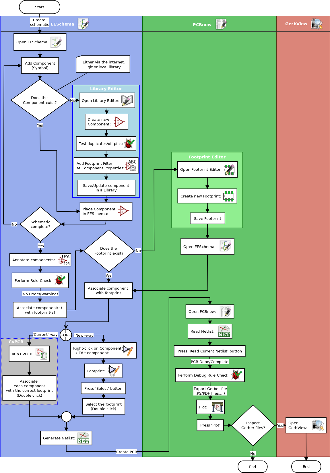
I was aware that KiCAD is bunch of programs unlike Eagle which has an integrated workflow, but KiCAD does a good job of organising files project wise which makes up for the fragmentation of the workflow in my opinion, the flowchart above which is from the
official documentation does a good job of explaining the workflow involved in KiCAD
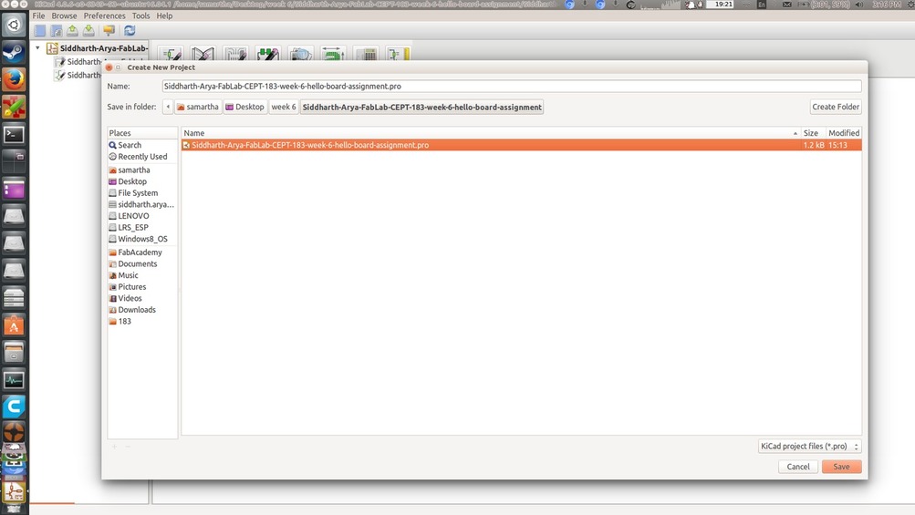
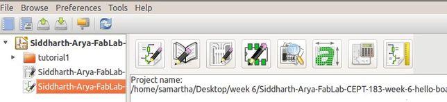
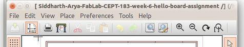
The first step is to create a project folder with a 'Create a new project' option, notice the file tree on the left, that can act as the project browser for switching between your schematic and PCB layout drawings and the Netlist

Click 'Yes' for the above warning, it'll create a new directory for your project
Schematic drawing
The first sub-program to use in KiCAD whilst doing a typical PCB design is the eeschema which is the first icon in the top toolbar

Eeschema opens with a 'page layout' meant to be printed out and thus will accept parameters like page-size and title-block details
Those parameters can be accessed through the page-settings icon on the top
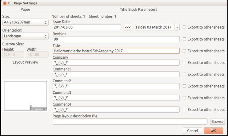
Here you can set the page-size, orientation and title-block fields like other CAD programs
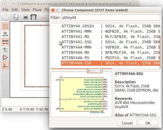
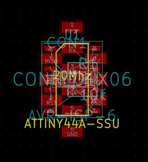
Components can be added by invoking the 'add component' tool which has the keyboard shortcut - 'a', I started by looking up the attiny 44 variant we had in our inventory, click anywhere on the paperspace after selecting thee component to place it.
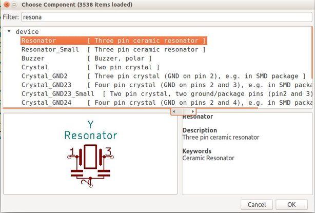
I continued by Adding the other components required for the hello-echo-board and all these components were present in KiCAD's library of components

The AVR-ISP i added from KICAD's library did not have an associated footprint, which I come to know later and use the AVR-ISP given in the Fab-library found in the
class notes page

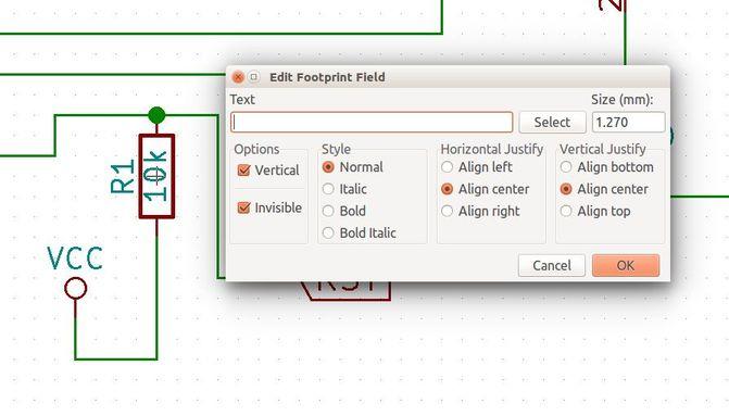
After all the components have been placed, hover over a component and press 'v' to edit the value of the component; like in this instance I've added the value of the resistor as 10k ohms
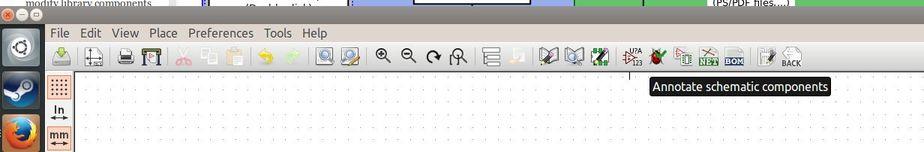
The next step is to auto-annotate all the components, where KiCad will assign names to components like R1, R2 to each component (R stands for resistors in this case)
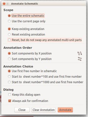
I chose all the default settings and pressed annotate, notice that in this window you can also clear out all previous annotations.

Now, all the components are annotated i.e named
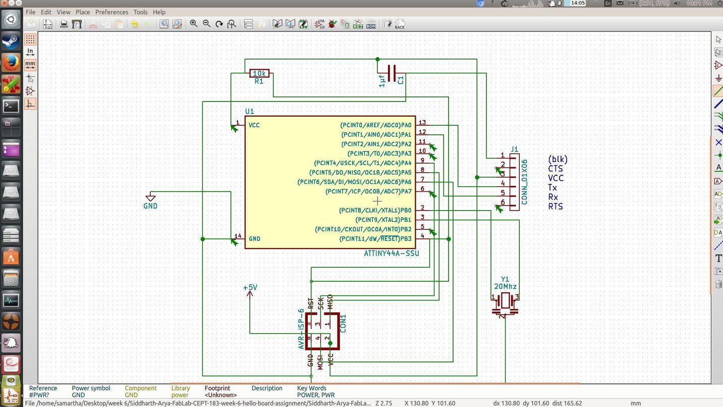
I got a little ahead of myself and routed all the wires in the sschematic like how one would route it in the PCB layout, but later learned about the 'global label' feature of schematics and redraw the connections
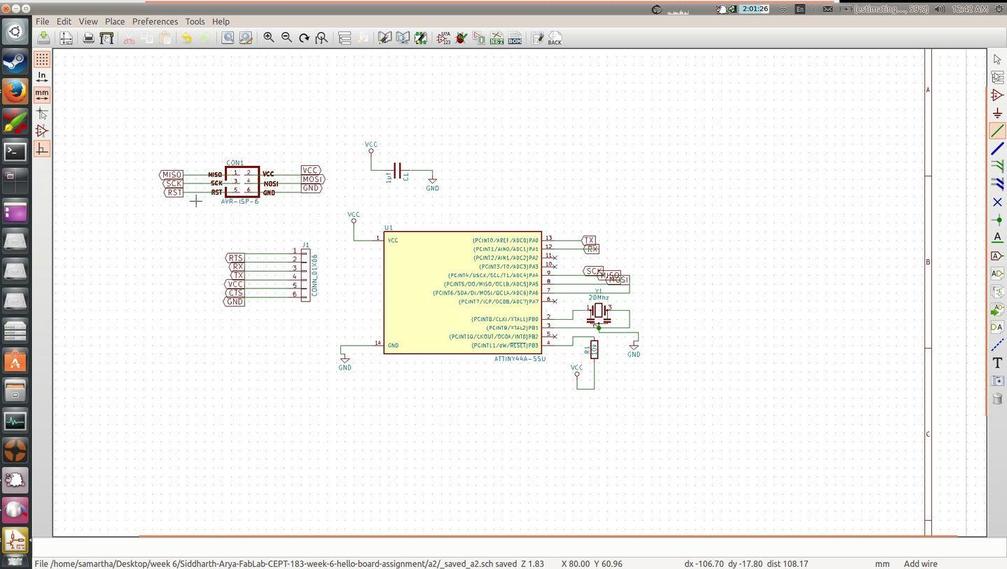
Here is the redrawn schematic, labels make the schematic much more easier to read

After doing the schematic the workflow suggests one to do a electrical rule check, the rule check tool is located in the top bar and has a bug icon.
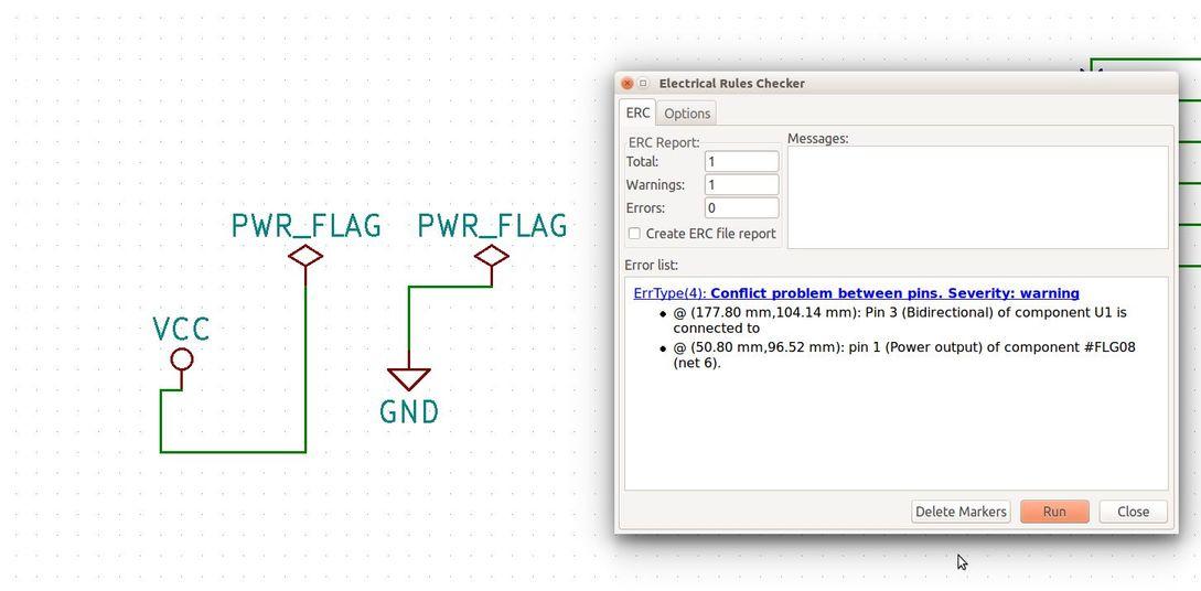
I googled the first warning I got about pins not being driven and learnt that power-flags need to be added to the schematic to tell KiCAD that power is coming from somewhere and KiCAD need not bother
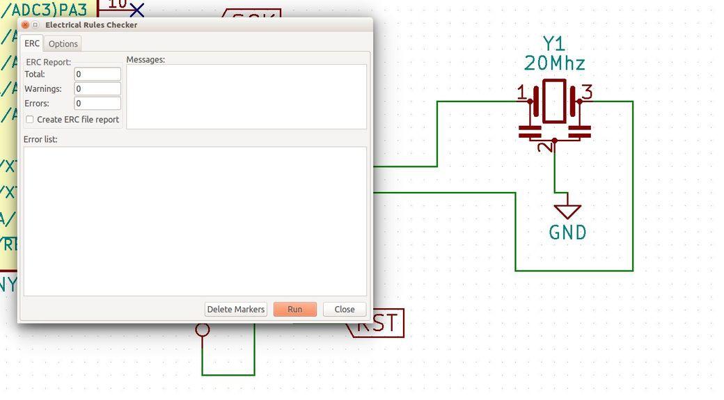
Another error still remained where the wire wasn't properly connected to the terminal of the resonator, when i redrew that line, the error resolved

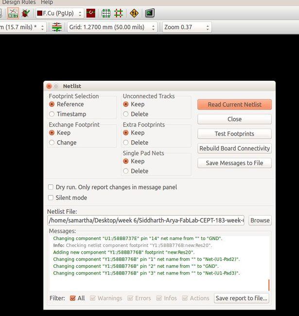
Click on the 'NET' icon to generate the NET list, the NETlist will be read by the PCB layout software
The old method of assigning footprints to components is throught the cvpcb tool found in the toolbar again
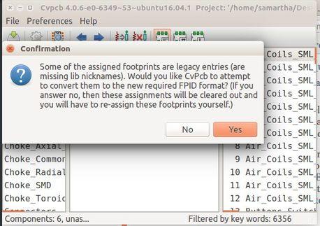
The footprint of the AVR-ISP was in an old legacy format and it failed to convert it to the new format

AS mentioned above, AVR-ISP is now without a footprint, now I decided to add the fab library to use the footprint provided there
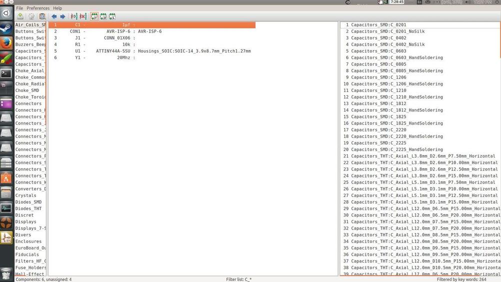
THis is the CvPcb interface where you can relate components to footprints from their respective databases

It's important to know that to finalize the assignment one has to double click on the footprint from the table on the right, this part is a little less unintutive
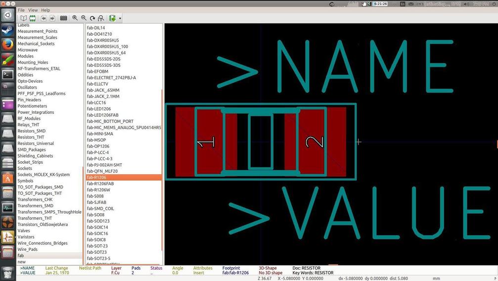
Adding the fab library of components and footprints to KiCAD

Open the libraries manager from Preferences > Library manager

Browse for the fab.lib, available from the class notes page
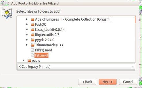
Similarly add the .mod file for the database of footprints provided in the class notes

IN the CvPcb a footprint can be previewed
To draw and add a new footprint

Start by creating a new library of footprints to save your newly about to be created footprint in, because one can't add footprints to KiCad's default library
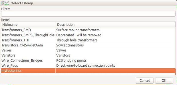
Next step is to select the newly created library as the 'active library'
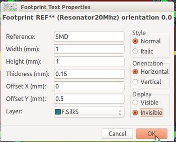
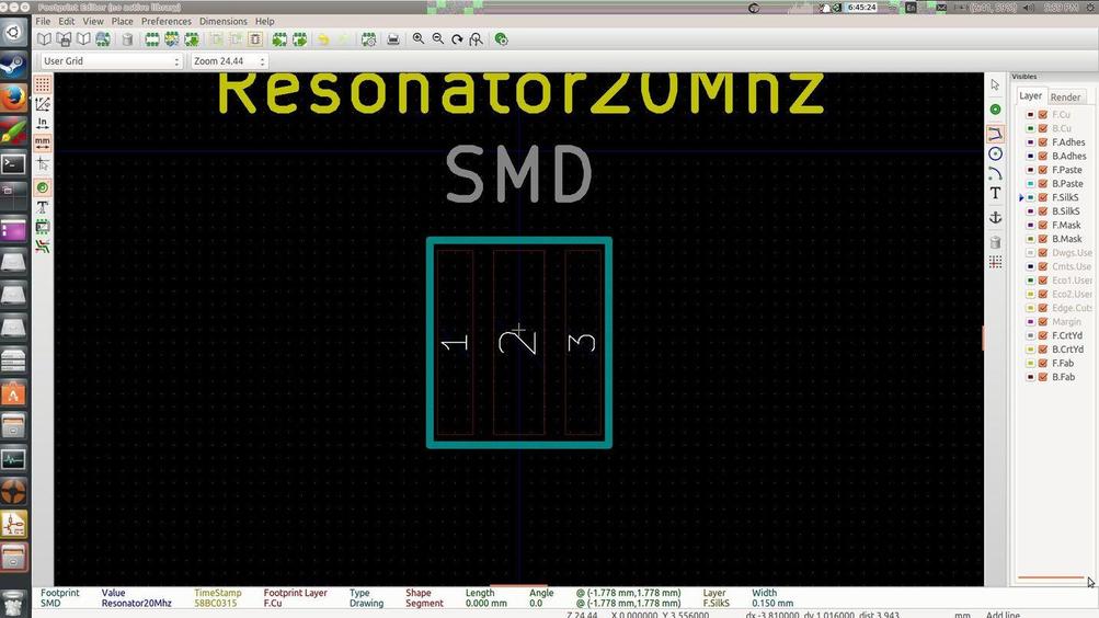
Set the footprint details with 'new footprint' such as 'SMD' and labels

In the layers tab, as of now, I understand that traces can only be drawn on 'Cu'(copper) layers and the board geometry can be drawn in the 'Edge.cuts' layer

The text you assigned will appear in the PCB layout in the 'Silk.screen' layer
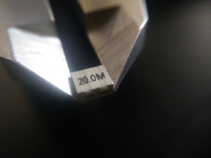
Next step was to measure the component so as to draw appropriate pads for it
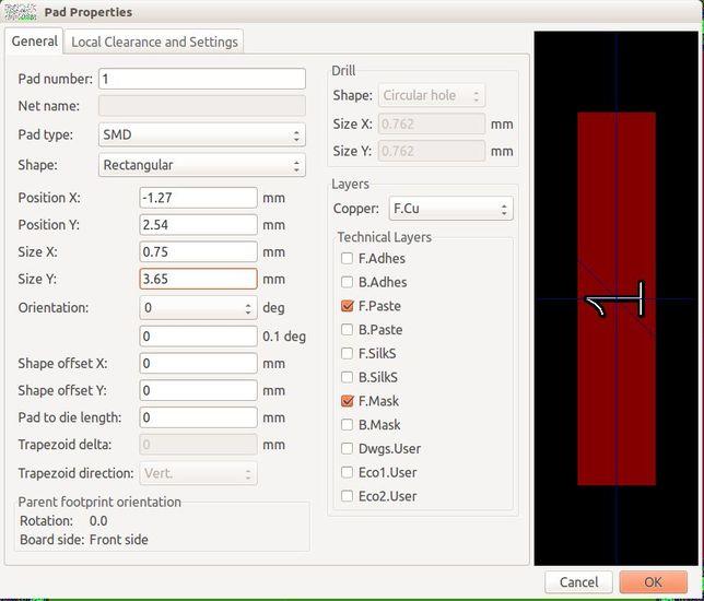
With 'add a pad' , you can set the geometry of the pad and place it on the drawing space with the help of the grid
Similarly, I added the 2 remaining pads and the outliine of the component itself
After saving the footprint, i returned to eeschema (the schematic editor) and hovered over the component and pressed 'f', this brings up dialog where you can assign the footprint, using cvpcb to assign footprints is the old method, this is the new suggested method
The new method has a built-in preview and a simpler set of tables to choose the footprint from

I next replaced all the footprint assignments to footprints from the Fab library with the new 'f' method

I opened cvpcb, just to check all the assigned footprints at a single glance. I guess the old method still has it's uses
Now, to commence the PCB design program, go back to KiCAD's main window and open 'Run PCB design' and choose the 'read netlist ' tool
PCBnew
the program will create components from the Netlist
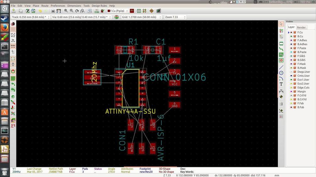
Hover over each component and press 'g' to drag them and space it apart
Next I changed the layer to 'edge cuts' to draw the boundary of the board

the components are now linked to each other with lines which are called a rat's nest lines which are a visual guide to see connections to be routed
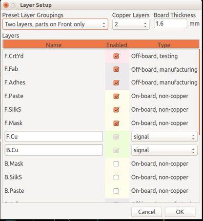
~ 'Layers setup' dialog seems to be the window for setting layer settings

~ 'Track widths' and clearances can be setup in 'Design rules editor' . The 1/64th bit determines the minimum clearance required. 0.35 is the least clearance I've been succesfu with so far

~ At this point, I've redrawn the hello-echo board without the LED and the button, to go back to the schematic and update the design a workflow called 'Backward annotation' is used as shown in the flowchart above
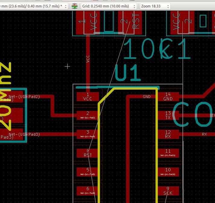
~ Manual routing for smaller boards is strangely joyful; like solving a puzzle

~ The redrawing of the hello.echo board is complete, I did take some cues from Neil's board to determine component placements
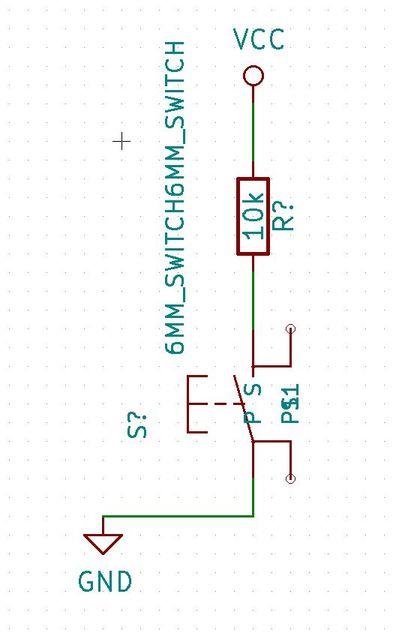
~ Now, to add the button and it's pull-down resistor back in the schematic.

~ Next, I've added the LED and it's pull-down resistor

~ Now, after saving the netlist again, if I update the netlist in the PCB drawing software, the new components show up at the bottom with their respective ratsnests
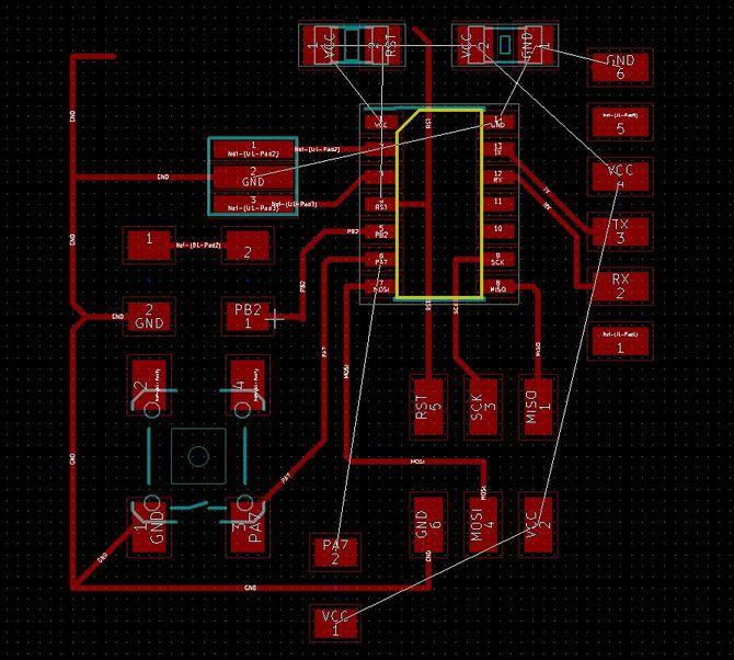
~Routing them in
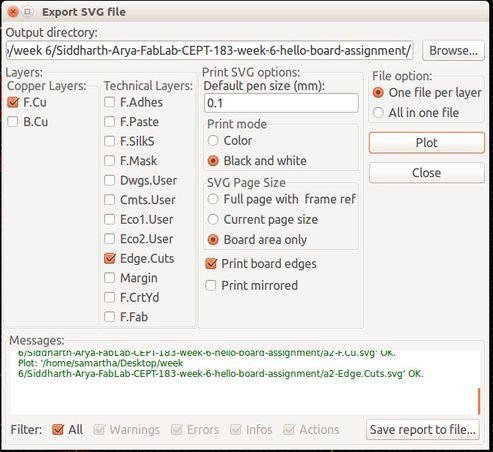
~ KiCAD, does not seem to have a PNG exporting option, so the workflow I followed is Export SVG > Import in GIMP at 1000 dpi > Export as PNG
~ GIMP is quite robust and SVG to PNG is a piece of cake
Milling and stuffing
On Milling The workflow was as folows
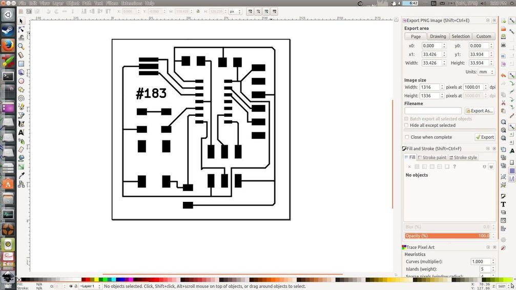
Export SVGs from KiCAD >
Convert them to PNG in Inkscape >
IMport PNGs in FabModules >
Mill the board in Roland Modela mx-20.
The workflow was exactly like in week 4.
- Fix copper board with Double-sided tape
- Set the origin
- Change the bit to 1/64th to mill traces
- check if the board is level
- Run the traces milling after setting the profile to 'mill traces (1/64) and choosing desired offset value
- Change bit to 1/32 " to cut out the board
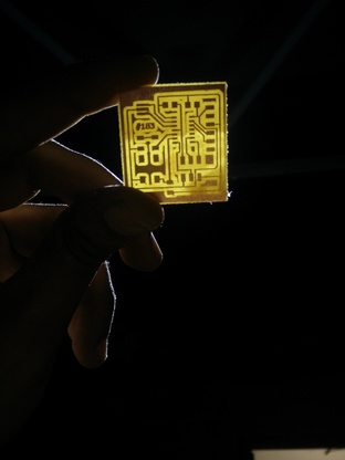
~ milling out the board has the same workflow as I followed in
week 4
ON Stuffing and soldering the workflow in stuffing and soldering is as follows
Setup Electronics workbench - SOlder station, tweezers, desolder braid and flux >
Ensure safety measures are undertaken - be aware of the solder gun tip >
Gather components >
Start stuffing
Things to keep in mind while stuffing and soldering
- The order in which you solder different components should be based on the layout of your board
- Pay attention to closely placed components
- consider space required for tweezers and solder gun to reach the pad
- I found the following order most convenient - ISP header, IC, FTDI header, button, LED and at last resitors and capacitors
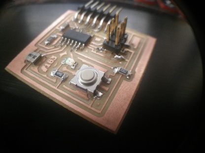
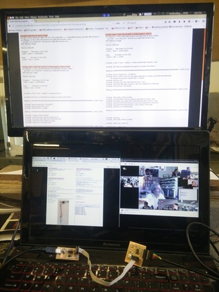
Hero-shot of the stuffed board
Programming
~ Programming the board with a FabISP, programmed Neil's example hello.echo code
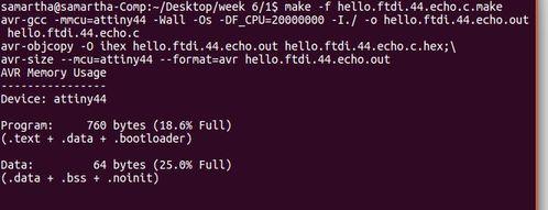
~configuring with 'make'

~ initialization failed the first time as the orientation of the ISP header cable was not correct
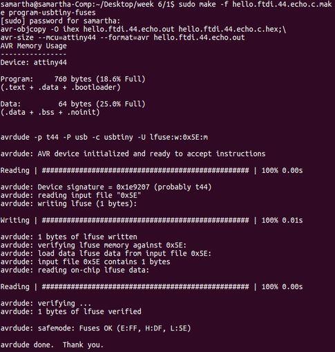
~make fuses went through
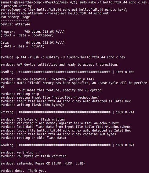
~ make hex compiled the code
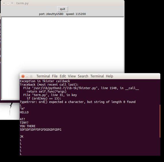
~ mmake program wrote the flash memory of the attiny44 seemingly successfully, but when I tried to use term.py to monitor serial communications, the attiny did not speak back :( . A problem to debug during embedded programming week. This week is done for now.
Other versions of the Hello.echo board i milleed, the last one is what I ended up using for week 8
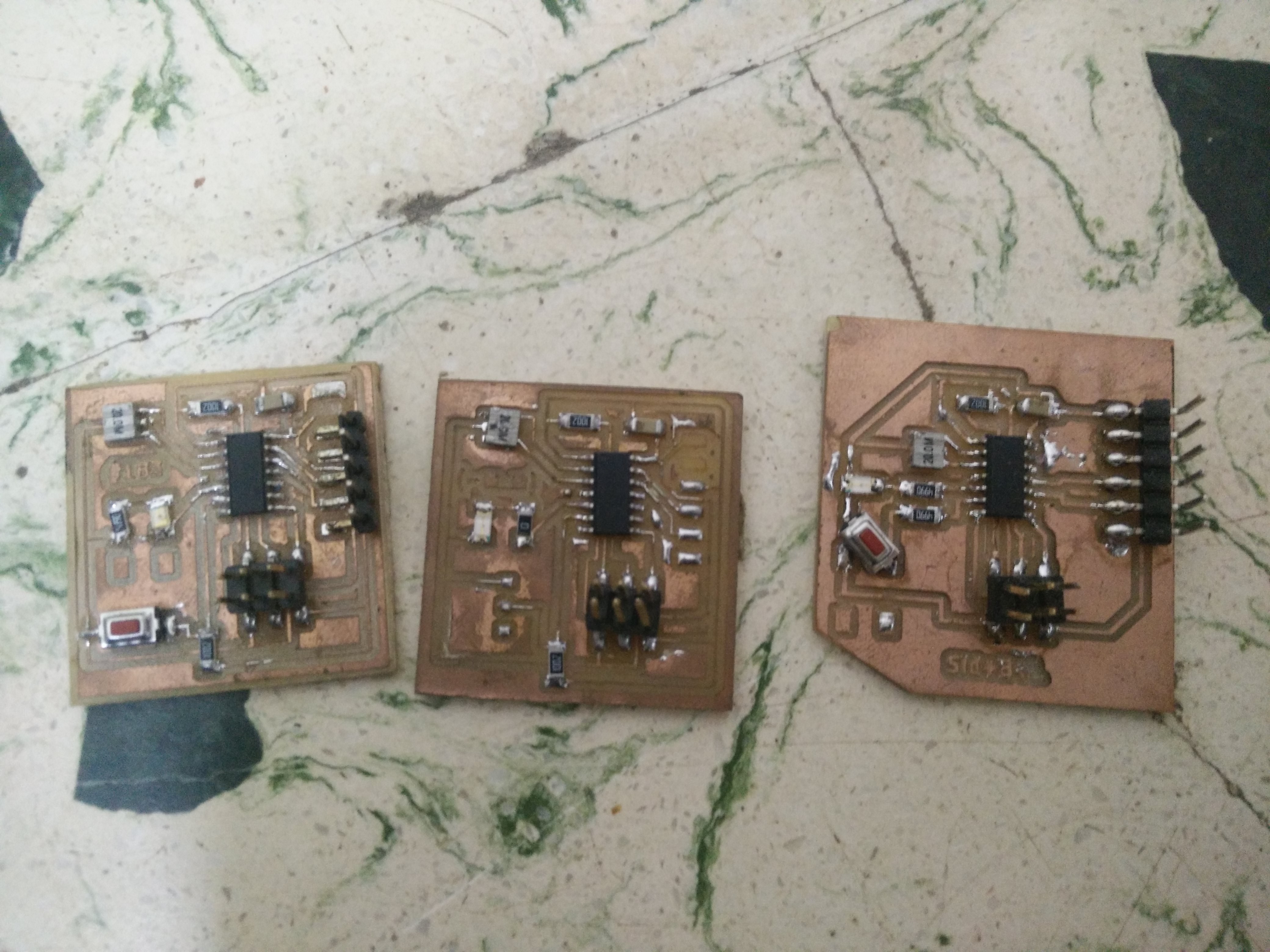
ver 2, ver3 and final version
File Downloads