Electronics Design
Designing my Hello_World Board with Eagle. I have chosen Eagle because it is very easy to learn, built up very logically and has a lot in common with normal CAD softwares. Our LPKF machine software goes along with Eagle, too. for small companys and private people it is free to use like for educational institutes, this is also a good reason to choose Eagle. Also I found this amazing tutorial from TU Berlin, which explains in a wonderfull understandable way how it works, where one has to be careful and about designing rules.'Technical University Berlin'First of all I would like to point to my 4th week electronic_production contribution.
Here you can find two 'tutorials' I wrote:
One instruction manual for our LPKF-milling machine and one Eagle manual. You can also find my basic understanding of wiring and designing a programmer circuit board.
But now you can read again the Eagle manual below:
First of all. For developing a circuit board you need to create 1. a schematic. Here you insert all components you need from libraries which contain the exact footprint for your component you want to solder. A wrong footprint can cause a circuit shortcut. Then you wire them in the right rules of electronic circuits. You can check the electricity with ERC at the bottom of your toolbar. After you wired all components you open 2. board design and now, you have to arrange everything without crossing lines. Because crossing or touching lines can also cause shortcuts or other malfunktions. You can check everything afterwards again and DRC, design rule check, too.
Start Eagle and a control panel will pop up and amongst others you will find in this panel the library and projects folder. Eagle works a bit different from user interfaces. You click a tool e.g. Delete and afterwards you select objects you want to delete. In the library you will find components you need, I will explain this later. In the folder Projects you will find your schemes and board designs. But now, you create a new file. Do not close the panel. It will close the whole program. In Menue/File selekt new/scheme and an empty page with toolbars will appear. Now I will explain the most importent tools and workflow.
 Add from library. With this tool you pick all components you need to build a circuit scheme. With the add tool you can place as many elements e.g. resistors as you need and with esc-button on your keyboard you finish this command.
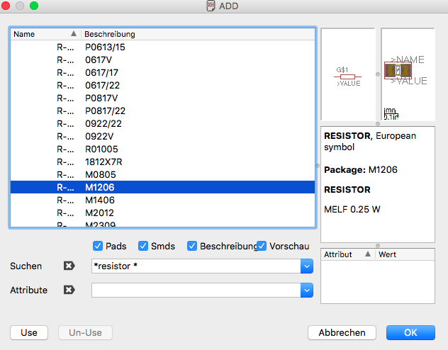 The library will pop up. You can look up in the list or write in search the name of the component if you don´t know the exact name you can write a partial name framed with *...*. After selecting your component the librariy window will close and the component will stick to your crosshairs. With left click on your mouse you place it.
After adding your components you can edit or move a component by clicking on or near its cross.
 Now, you can change the name of your component to be able to recognize it later on your board.
 With change value you can set the right value for each component, this is very important, because if you want to read your scheme years later or somebody else wants to read it and build it, you should know which components you used.
 If you need more then one component of one type e.g. resistors, then you don´t need to add all of them from library. You can just copy the first one and adabt the values and names.
 If any component or wire is wrong you select delete from toolbar and with clicking on wires or elements they vanish.
 Move is a very important tool, too. You select move, click on a component you want to move. It will stick immediatly to your cross hairs and you place it somewhere else. If it has the wrong direction, you can rotate it with the right click on your mouse or two fingers click on your trackpad.
 But you can also rotate with the rotate tool.
 First you have to select the command you want to do e.g. Delete. Afterwards, you select group tool and draw a frame around a set of elements you want to delete. They will change their colour and with the right click on your mouse you can choose delete: group. To finsh the command delete you press esc.
 Before you start to wire them click on grid to set the grid dimensions. I like to use mm and first I took the preset size 2.5 mm.
Later on in board file, I switched to finest grid to be able to wire them more accurate.
Before you start to wire them click on grid to set the grid dimensions. I like to use mm and first I took the preset size 2.5 mm.
Later on in board file, I switched to finest grid to be able to wire them more accurate. With layer you can make layers visible or invisible.
  With Net tool you can wire all components.In the above command line beside the grid icon you will see all designs of wiring.
 After wiring it is possible that you can´t read the names and values of your component anymore, too many overlapping labels. With smash you can uncouple them from the components and set them in a readable way.
  But you can also make the informations about values and names invisible see them only with the icon Show. With this icon you get all informations about this element.
 Now, switch to board layout. You will find this icon in the above command line where the magnifiers are.
All elements will be set beside your outlined platform with the wirings . You have to drag them inside this outline. Keep your scheme open to be able to check the wiring. I didn´t use autoroute you will find at the bottom of the toolbar. I set all wirings by my own, it took a while. Again, you place all components with the icon move. And start routing on top layer with red lines on bottom layer with blue lines. You can see all layers by clicking on layer icon.
 With Ratsnest you set automatically the shortes ways between the conected components. It is helpfull to do it frequently to organise the board.
  Routing demands a carefull settling to receive a connection between two components. It is easy to recognize if it didn´t work out, the routing line doesn´t stop to route, furthermore it sticks to your curser. Also you will hear a sound when routing works out. For this part of work it is good to adjust the grid.
You can´t delete the red lines anymore you just can change them into bee lines again through clicking the Ripup icon.
Routing demands a carefull settling to receive a connection between two components. It is easy to recognize if it didn´t work out, the routing line doesn´t stop to route, furthermore it sticks to your curser. Also you will hear a sound when routing works out. For this part of work it is good to adjust the grid.
You can´t delete the red lines anymore you just can change them into bee lines again through clicking the Ripup icon. If you click on change tool in the toolbar you will get a list of possibilities like diameters, Font, Layers..
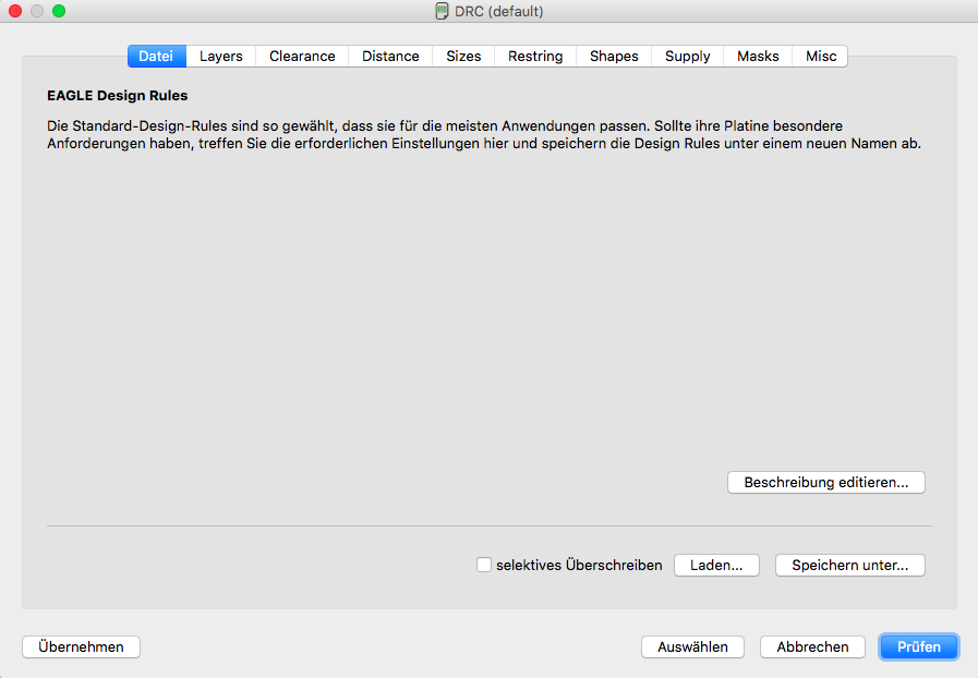
 Finally, you should do an electrical wiring check. With the DRC check you can see if your board matches the design rules. Please see below at the bottom how I checked my DRC and ERC
 Finally, you build a polygon around your board, to be able to use your board as GND. In the top symbolbar you can choose the width of your polygon, if it as filled up, hatched or cut out and you can choose Isolation size of your vias. Click again on Ratsnest and you will see that the board will filled up with red colour.
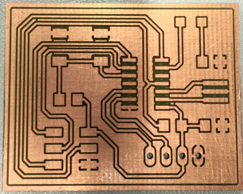
 After finishing the board design you can send it to LPKFCircuit Pro for milling. Choose Cam icon in the top Symbolline. A window will pop up and asks for executing the job. Select in Menue/File/Open/Job/LPKF_Export.CAM. Then click Execute Job. LPKF Circuit Pro is a milling software for our LPKF millin machine. Now, you can follow the above instructions.
Now, I would like to look more into the components:
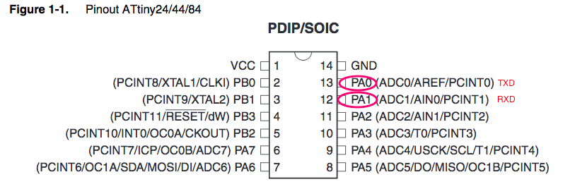
The center of this board is ATtiny 44. It has 6 more pins and has more Input and Output pins. Also the allocation of Vcc, Reset and GND is different.
With add I opened the library and insert one component after another. I wrote the name of the component in the empty field search or suchen pressed return button and a list came up for example header list. Then I chose one 2x3 pin header in 2.54 grid and as soon as I pressed the 'ok' button I had a floating symbol sticking to my curser. I just had to place it .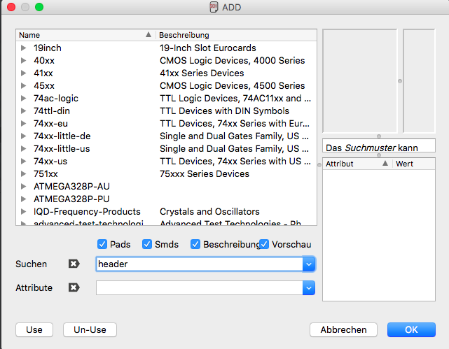
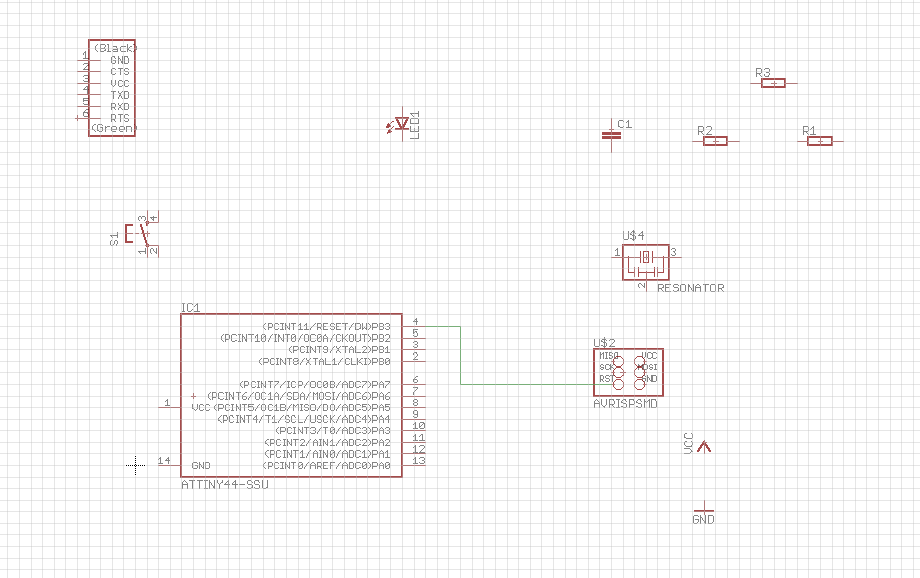 After inserting all components I needed, I started to wiring them.
 After wiring I did the electrical check to see if I have produced some shortcuts. Then I switched to board layout.
Here I had to pull all components in the frame, they were wired with yellow air lines. That means I had to route them.
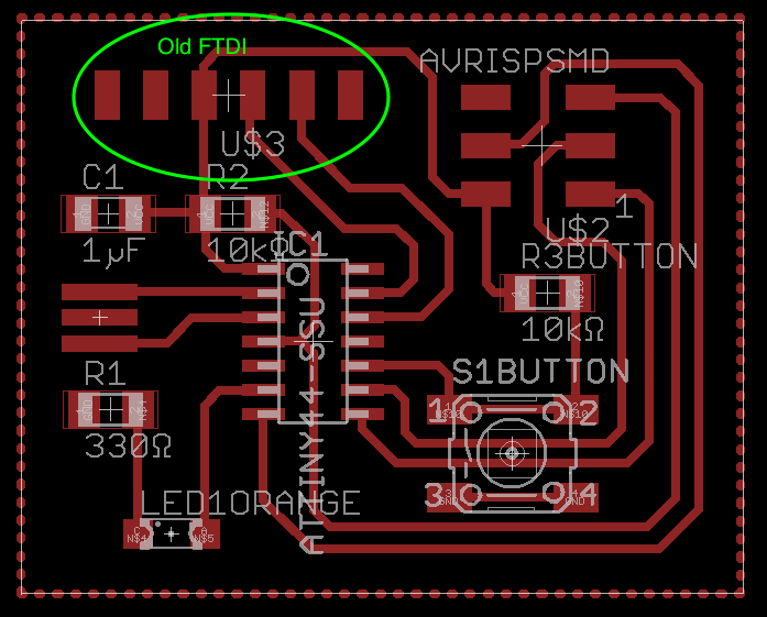
I routet the components trying to avoid overlapping or touching. Sometimes I had to ripup one routing and got a yelloe air line again. You can´t delete a route, you just can rip up. 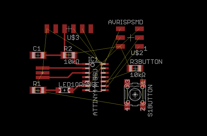
If you want to exchange a component or to wire up differently then you have to switch to schematics again, do it there and come back.
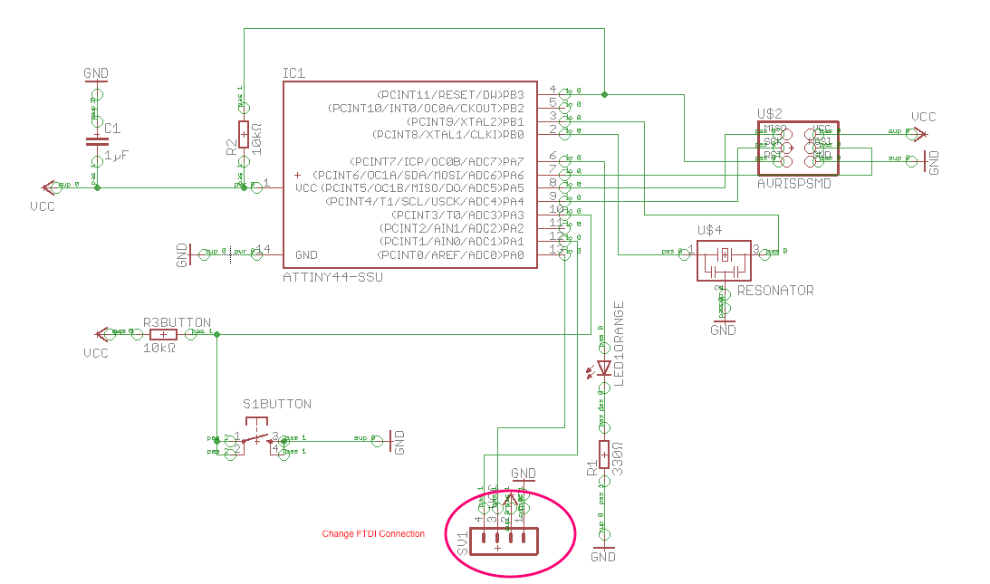 Now, use ratsnest to see if there are air lines left.
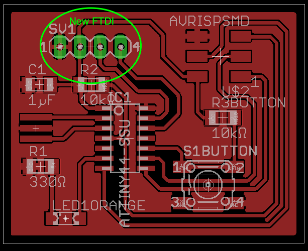
I did the DRC and the ERC. What does it mean? DRC is a design rule check to be sure that the designed board will be produced without failure or violation. The DRC is written in a separate file and should be located in Eagle bundle named 'default.dru'.And the ERC is the electricity check, that there are no short cuts:


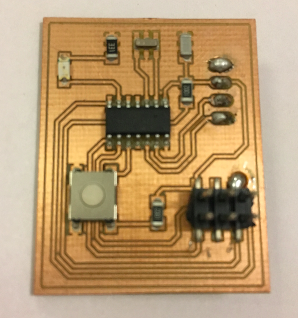
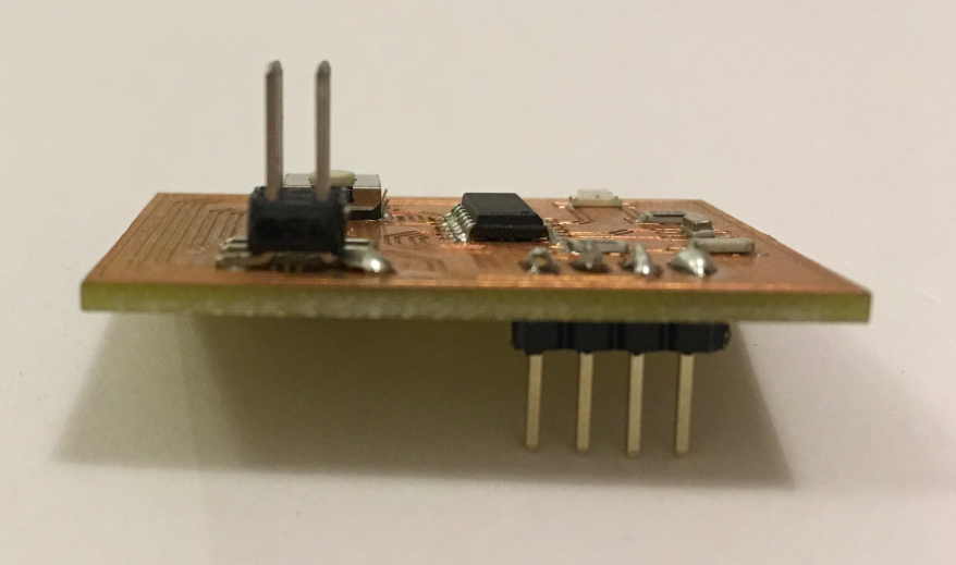
Please see below my milled Hello board:
Fab-Academy Tutorials
If you want to download my board layout: Aleks' Hello Board
Aleks' Hello Board schematics
Every resonator has it's own footprint and as I' got a different resonator I wanted to adapt the footprint and import a different symbol. But anyway, even with the bigger footprint it worked out:
Aleks' Hello Board Resonator Footprint
Aleks' Hello Board Resonator Footprint schematics