Week 6
Electronics Design
Assignment
- Redraw the echo hello-world board, add (at least) a button and LED (with current-limiting resistor)
- check the design rules
- Make it
- simulate its operation
Week workflow
Here is how I see the week's flow :

Flow chart for this week
Table of content :
STEPS
Drawing the schematic
First We download and install Eagle.

Eagle Logo
After we've done that we start a new project.
I'll name mine "My Echo HelloWorld Board"
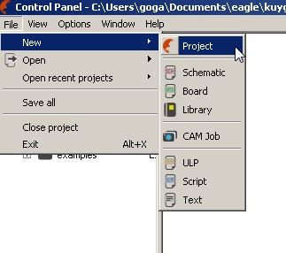
Starting a new project in Eagle
And in this project, we create a new schematic :
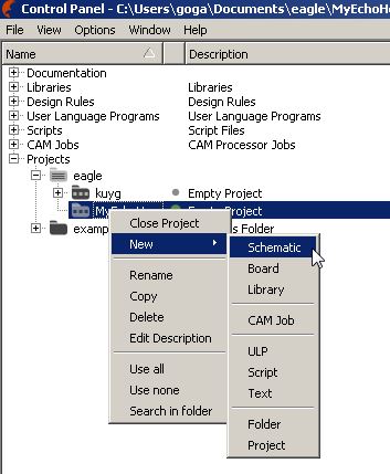
Starting a new Schematic in Eagle
We get the schematic interface :
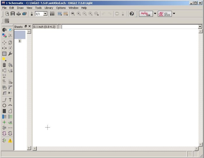
Eagle's schematic interface - White Canvas
Then we have to add our components.
But before we do that, we need to add the library that contains our components. The fabacademy provides us with a nifty
fab.lbr
library that has all the components we need.
We import it in the install folder of Eagle, for me it's C:\EAGLE-7.5.0\lbr.
Then we tell Eagle to use it :
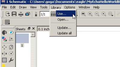
Specifying the use of the fab library
Once we've added the fab library we can go fetch them and add them on the canvas :
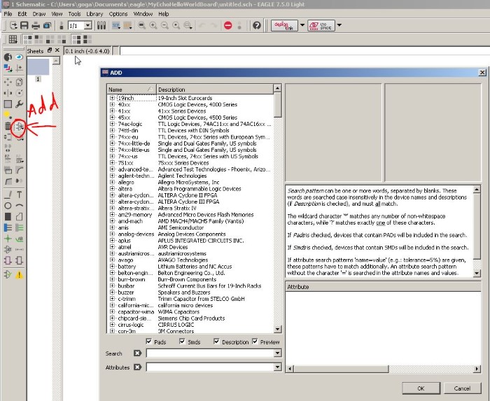
Adding components
We then go to our fab library and add the components we need :
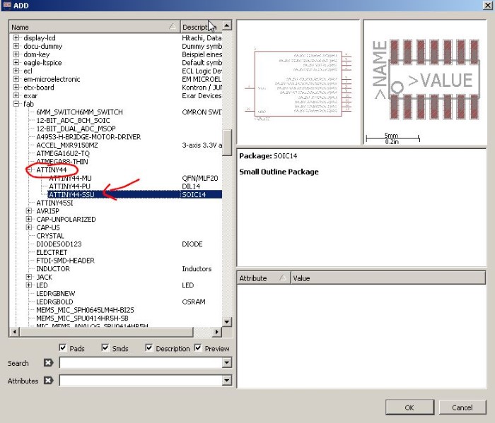
Selecting the t44 and adding it to the canvas
Sometimes there is several choices for the parts, for ex the LED :
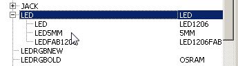
Several choices for the LED
I choose the LEDFAB1206 cause I like the idea of being able to put a trace in between.
As required for this week's assignments, I add a button and a LED :
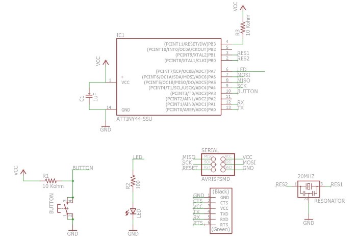
Schematic completed with added button, pull-up resistor and LED
I check the ERC errors (I guess that ERC stands for Electrical Rules Control or something like this) :
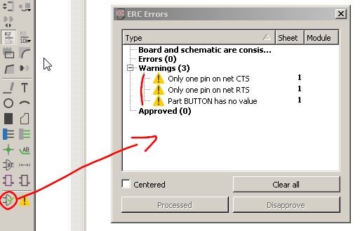
Checking the ERC errors
Two warnings are just telling me that there unconnected pins, which is indeed the fact.
And the button warning is ok I guess since there is no value to this button component
Now has come the exciting time of the incredibly more fun game than tetris or sudoku : routing and PCB layout
Laying out the PCB
Clicking on the "board" button brings us to the PCB layout window :
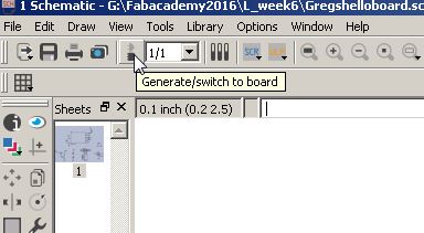
The board button in the schematic window
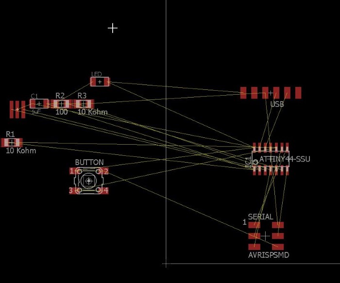
The PCB layout working space canvas
Let me see, do I feel confident ?... hmmm. Alright, I decide to try to make my own design.
First I set up my design rules :
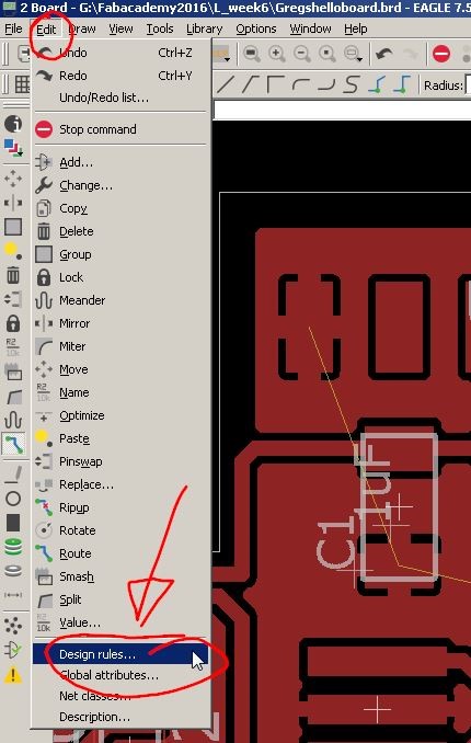
Checking and setting the Design Rules
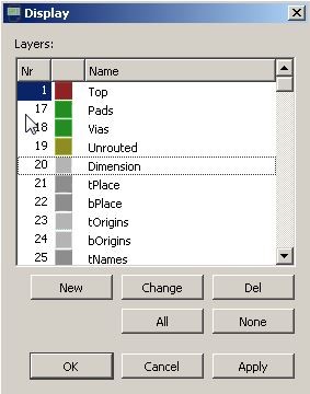
I want only one top copper :
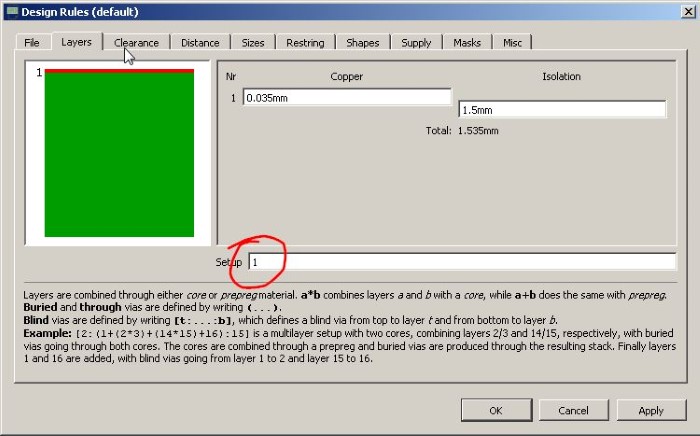
Only Top Copper
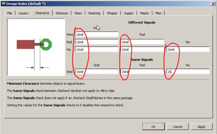
Because we use a 1/64 mil bit for milling the traces, which is a shy 16 mil, I define my clearances to 16 mil :
Setting the clearances to 16 mil
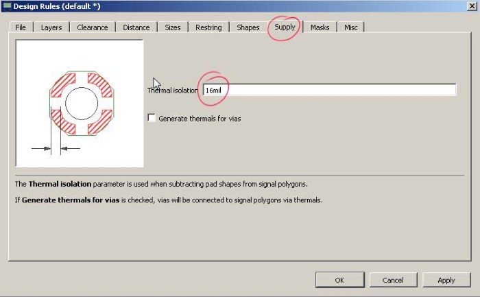
Since I'll be doing a ground plane, I need to define the clearance also fo the heat dissipation restriction feature :
Setting the clearance for thermal isolation
Since I'll be doing a ground plane, I need to define the clearance also fo the heat dissipation restriction feature :
Setting the clearance for thermal isolation
I get to a point where I need to connect two ground planes over a trace :
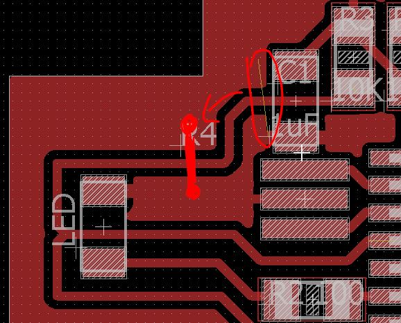
How to connect those grounds?
I decide to add a 0 ohm resistor.
I feel like I'm cheating but I decide to live with it, there's more profound issues in life.
I need to add the fake resistor to the schematic :
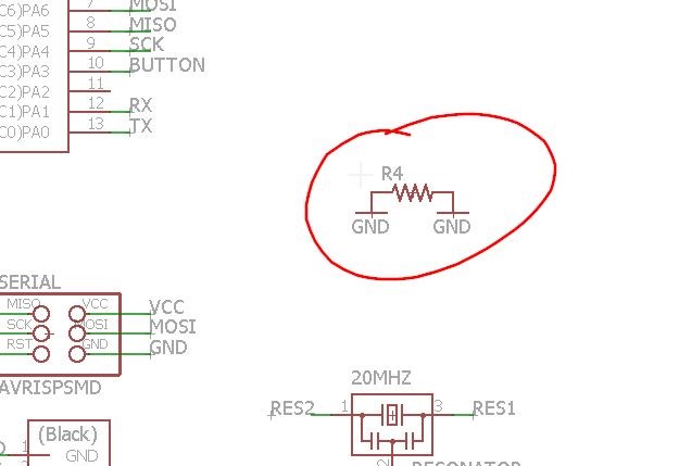
Setting the clearance for thermal isolation
Then I place it on the completed layout, tada ! :
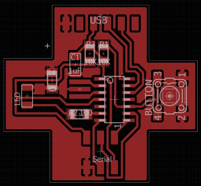
Completed pcb with the zero resistor
I check if everything is okay according to the design rules :
Checking the design rules
What??? Errors :
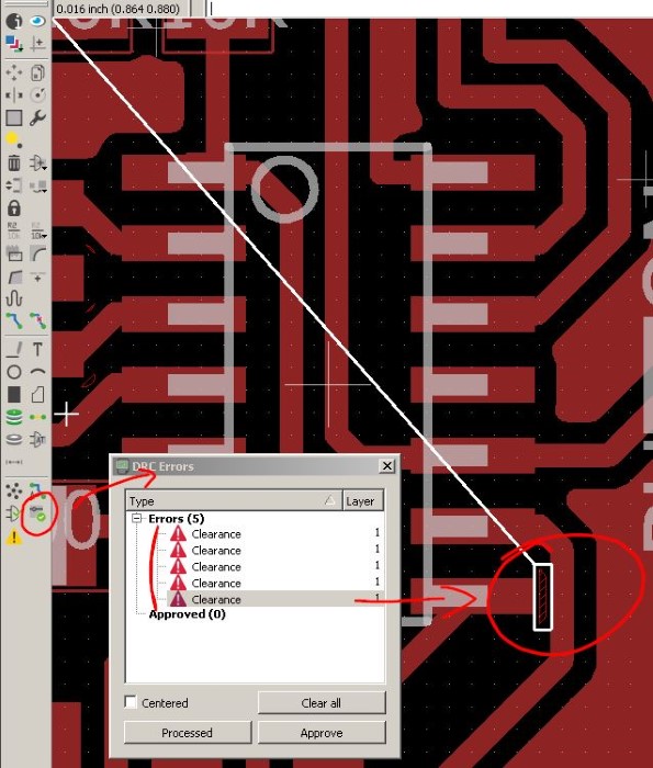
Design rules check errors
Oh! Okay I know how to fix this! Just a little bit of moving around for our milling bit to be able to cut here
There's still a yellow line between the pads of the resistor but I feel lazy to struggle. I know it's okay.
I feel happy and I'm all excited about milling it!
I first need to generate my PNGs
>I then select only the copper layer :
Selecting the top copper layer
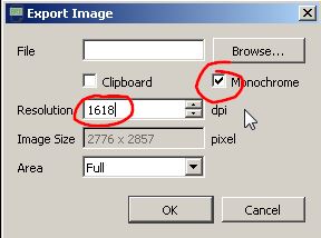
And export as an image :
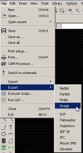
Exporting as a PNG
In monochrome mode. I also choose a golden 1618 dpi just to bring me luck
PNG settings
Some basic raster image editing to generate the outline, and I'm ready with my two PNGs :
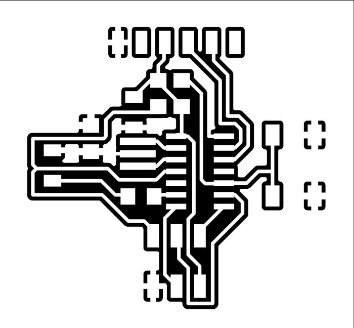
traces PNG
Outline PNG
I'll just make sure the scale is alright :
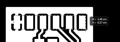
Checking the Scale
1.4cm around the FTDI pads, exactly what we want. Good!
Milling
I'm then going to go through a process that has been documented in detail during a previous week : Electronics production
I'll just put here the important steps
First, generating the path in the fabmodules didn't work completely. There was some merging :
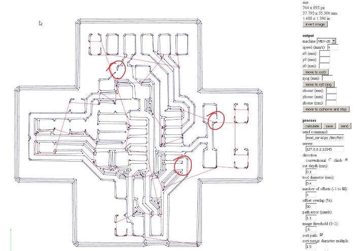
Merging problem
Why is that? I don't really know since we have a clearance of 16 mil everywhere and the bit is 1/64 = 15.6mil.
Maybe something to do with the "path error" parameter
I decide to fix the problem by editing the image. I expand the black area in the traces PNG by one pixel. It works.
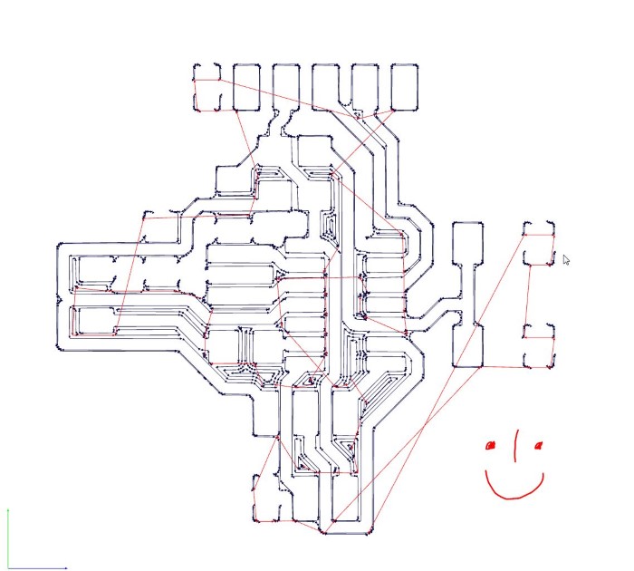
Merging problem adressed
Let's go for some milling on our Roland Modella MDX-20
Milling our board
And there we are :
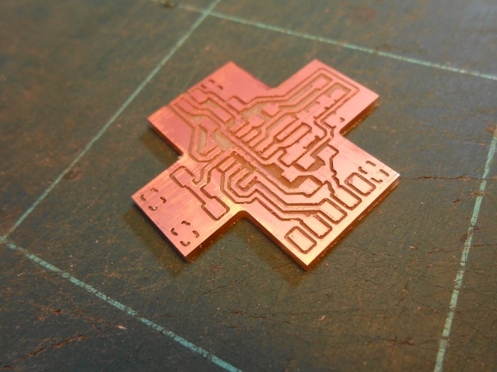
Board freshly milled
Soldering
A little bit of soldering and...
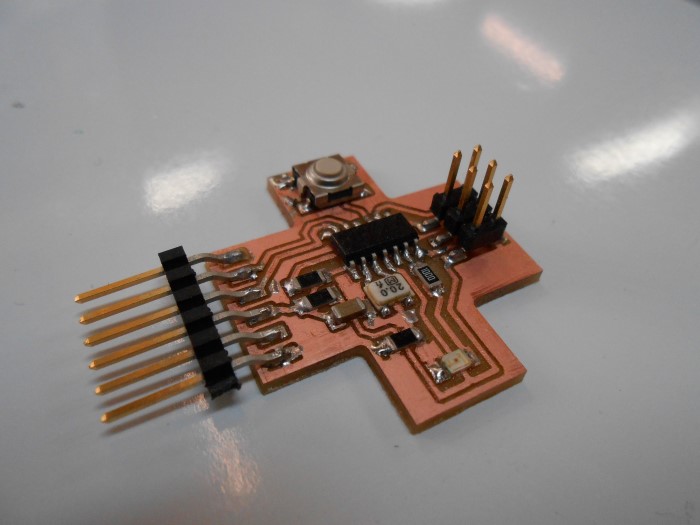
Hero shot of the board
Just two notes on the soldering :
I had a doubt about the 10k resistors in the drawers, so I checked :
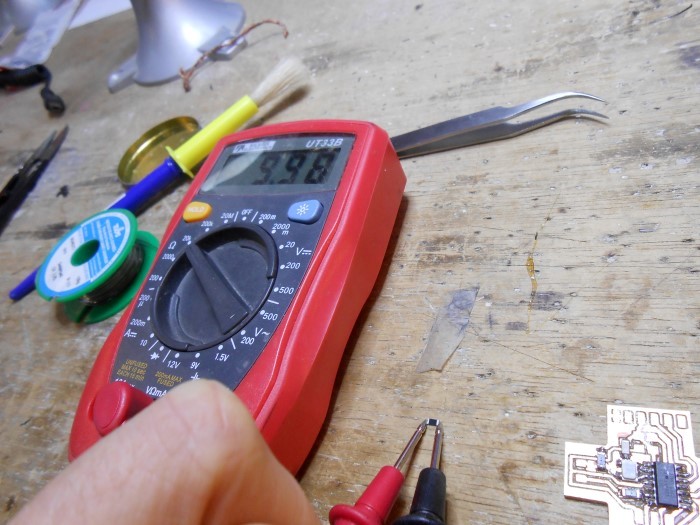
Making sure that we have a 10k ohms resistor
Also, I was unsure about the orientation of the switch, so I checked the datasheet
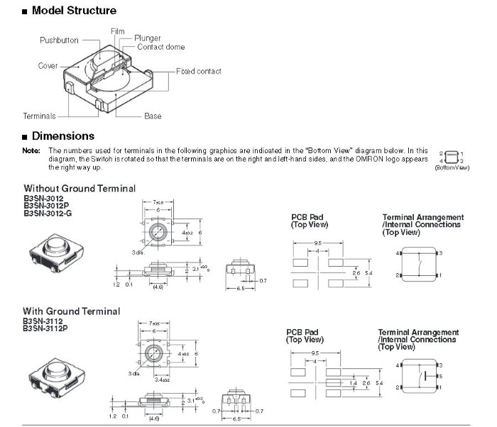
Checking the datasheet of the switch
At this point I can't resist the temptation of checking if the board is working so I try to do basic communication with it
Testing
I then hook it up to the avrisp as follows :
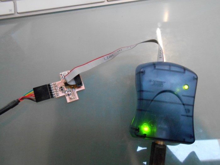
Establishing connection through Avrisp
and type in a terminal :
avrdude -c avrisp2 -P usb -p t44
And it works ! :
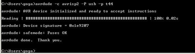
Working connection through AVRisp mkII
same thing with my FabISP :
avrdude -c usbtiny -P usb -p t44
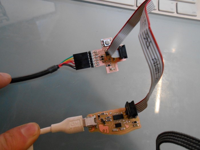
Establishing connection through the USBtiny
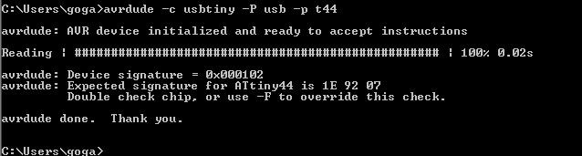
Working connection through the USBtiny
I notice however something weird with the signature. I'll invesrigate thsi later
Happy family board shot
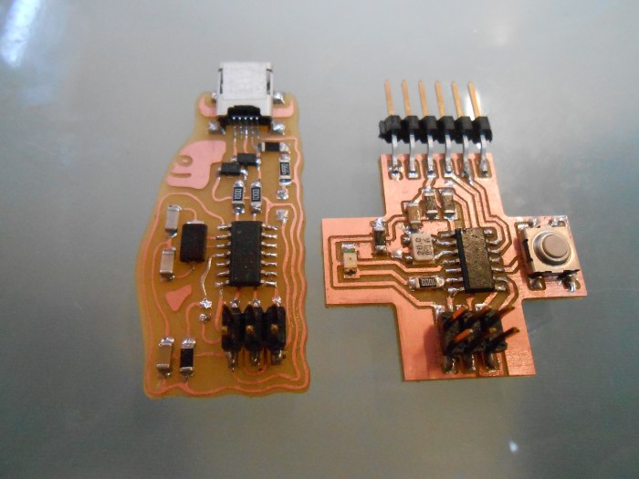
Happy Board family
Simulating
Finally I wanted to try the simulation from Eagle but I get a error message :
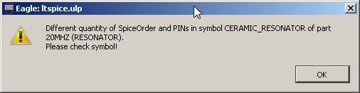
Error when simulate
I quickly check on forums about this error, and it looks like it's not something obvious.
I decide to give that up since I don't have the time right now
I still wanna play with the simulation tool though. So I draw and simulate the pull-up resistor system in LTspice :
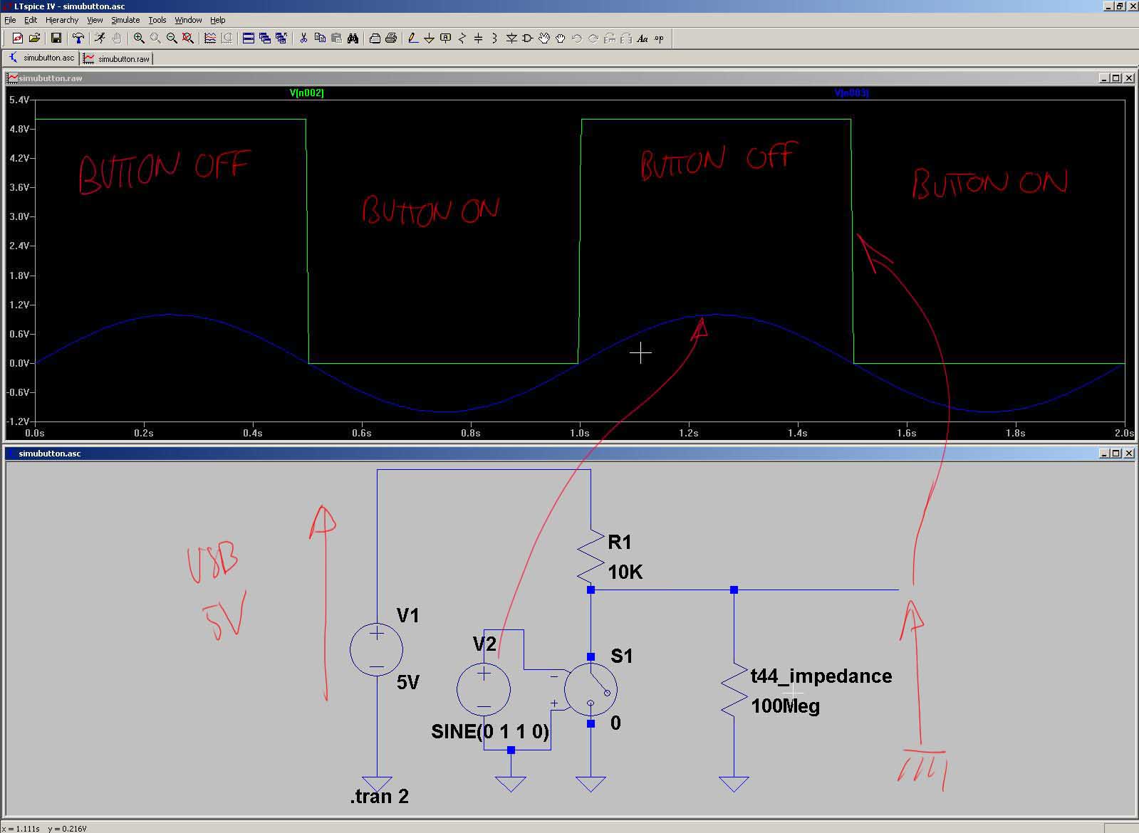
Simulation in LTspice
To emulate the button ON and OFF I didn't find anything better than hooking up a sine to the driven switch.
And I think I found the impedance of the t44 on the datasheet, p 177 :
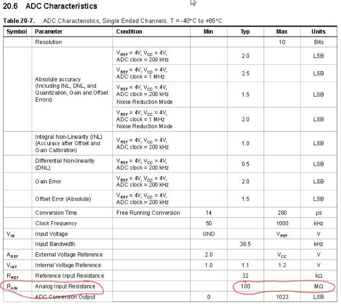
Impedance of t44 in pin
We can see that as soon as the Button is Off, the voltage read by the t44 is quasi-5V, i.e. "High", pulled-up by the 10k resistor.
It is in fact, since we have a voltage divider, expressed in kohms : 100000/(100000+10) = 4,99V. Perfect "High" state
If we check the current when the button is on to make sure we don't use too much power :
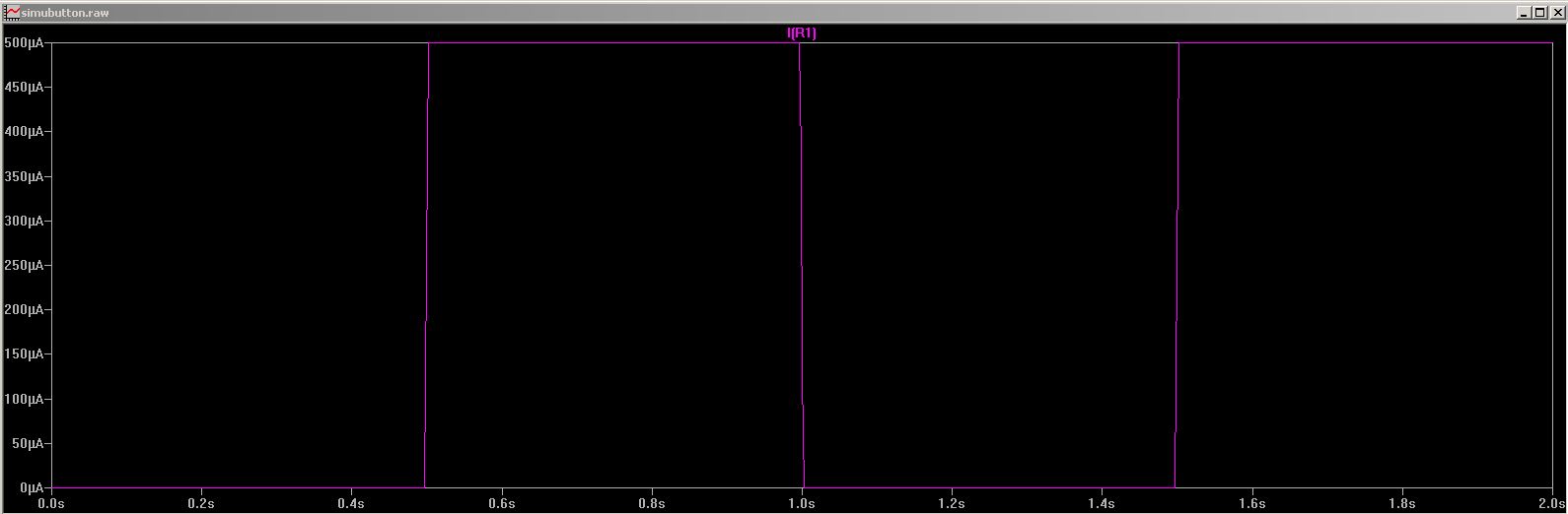
Current in pull-up resistor
We read 500uA, which is exactly what ohm's law says : V = R.I => I = 5 / 10000 = 0.00005 A
That means P = R.I.I => P = 10000*0.00005*0.00005 = 25 micro Watt.
I think we won't blow the house's fuse...
Sources Files
Here are the sources files of the projects I talked about on this page :
EAGLE - Schematic
EAGLE - Board Layout
PNG - traces
PNG - Outline
LTSPICE - Pull-up simulation
Conclusion
***