Week 15
networking and communications
Assignment
- design and build a wired and/or wireless network connecting at least two processors
Week workflow
Here is how I see the week's flow :
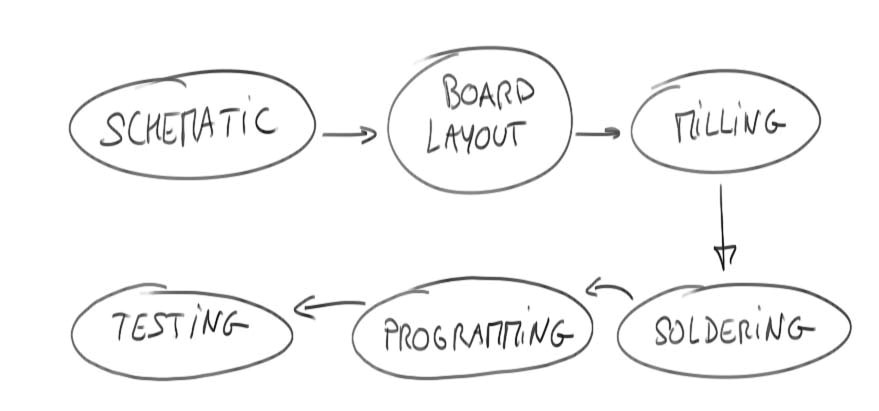
Flow chart for this week
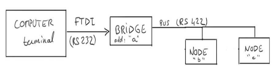
To get closer to this week's network and communication concepts and potential, I feel that recreating from scratch my own version of Neil's Hello.bus would be just fine.
So I will make three boards : a bridge and two nodes, all three linked with a bus and ATtiny45 based.
The physical link will be a 4 wires ribbon cable
The communication protocol will be serial at 9600 baud
The addressing will be done by hardcoding a different address in each firmware of each microcontroller
The testing will be done by typing board addresses into a terminal on the master computer and waiting for their respective answers.
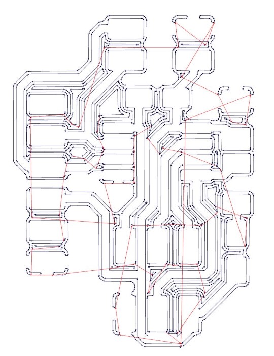
Here is a diagram of the architecture of my network :
Flow chart for this week
Table of content :
STEPS
Schematic
I draw schematics in Eagle :
First, the bridge board :
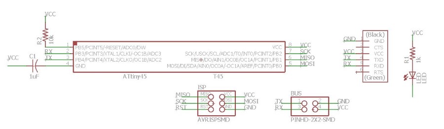
Schematic of the bridge board in Eagle
Then the node board, which is basically the same as the bridge board wigh the FTDI connector removed :
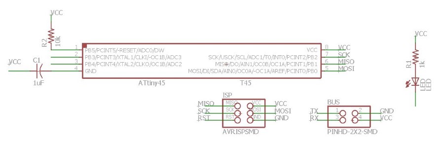
Schematic of the node board in Eagle
Board Layout
From the schematic I layout the boards :
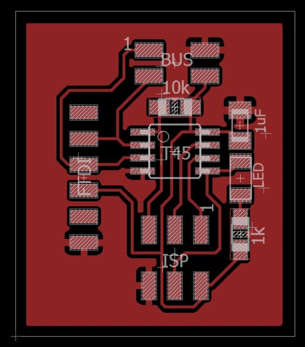
Layout of the bridge in Eagle
Again, the node board is the same as bridge board with FTDI connector removed.
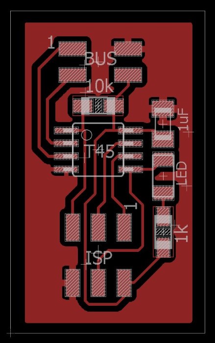
Layout of the node board in Eagle
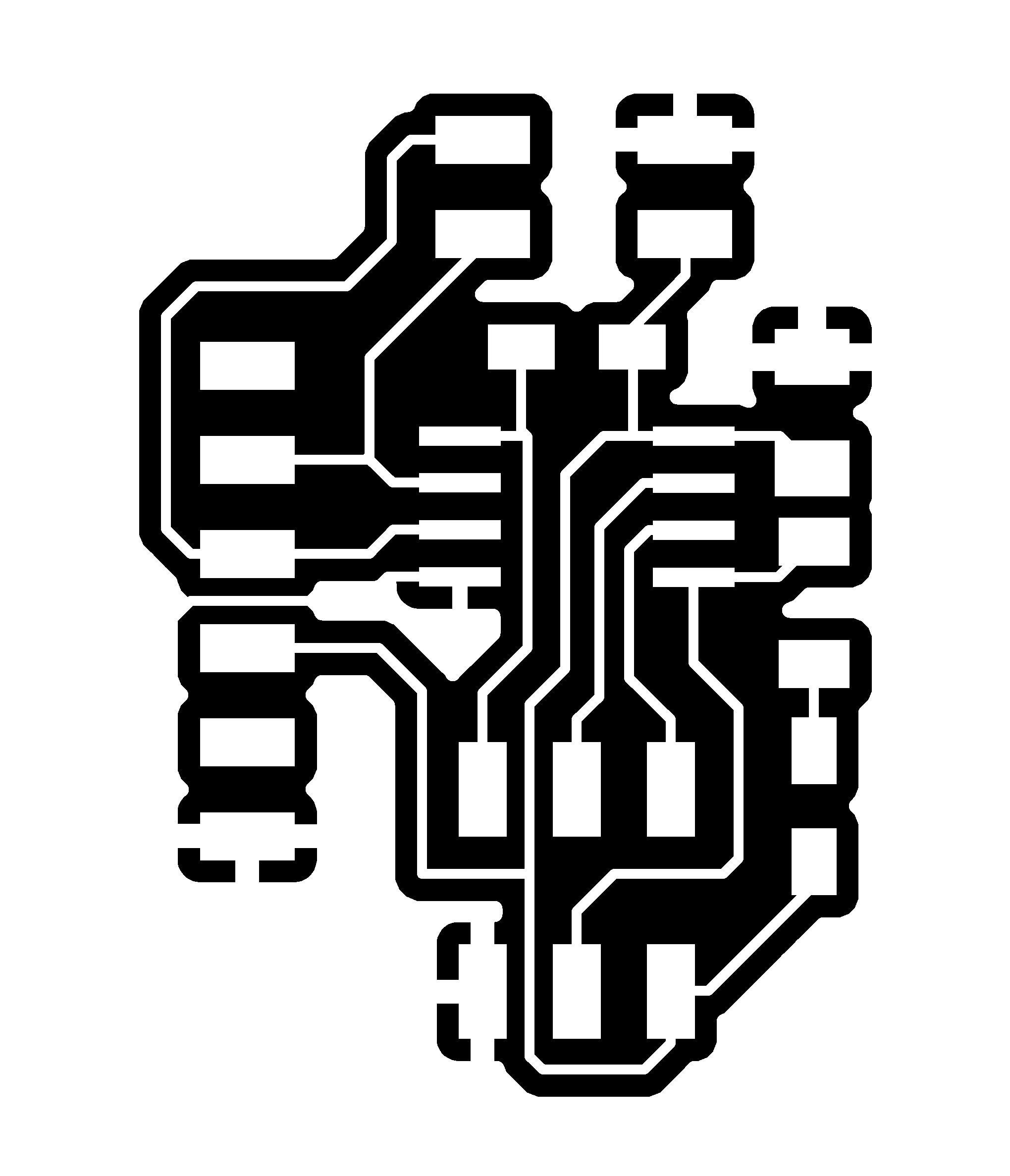
Then I export a black and white PNG representing the top copper layer
the bridge board :
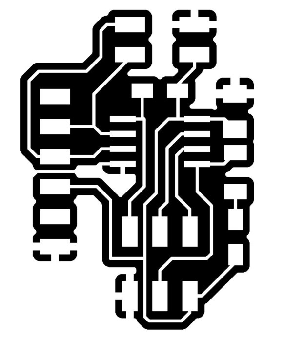
The bridge board traces as B&W PNG
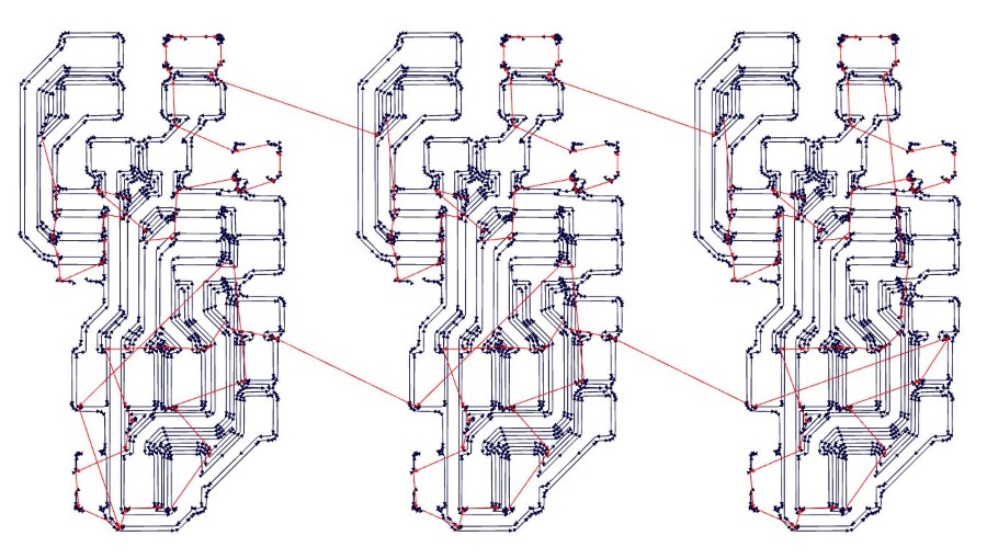
I duplicate the node traces in three and make it only one PNG to mill three boards at once.
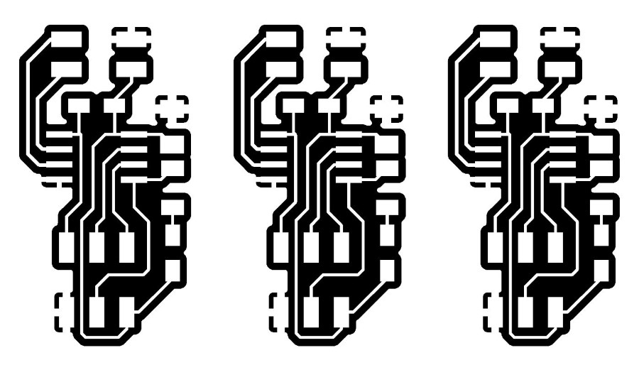
The node boards as B&W PNG
Milling
I use fabmodules to generate the gcode :
The bridge board :
Toolpath in fabmodules for the bridge board
And the node boards :
Toolpath in fabmodules for the node boards
Unfortunately, the third node board was milled outside of the stock I had, so I got only two.
Also, at some point, the monofab failed. It was stopping in the middle of the milling process saying it has not enough power.
It's true that it has been doing a lot of unexpected vibration noise recently.
So I suspected it was coming from the rotor.
I find out that the rotor axis is worn out (not anymore circle) where it goes in the bearing.
And the bearing itself, a simple plain bearing that looks like brass metal, is very loose :
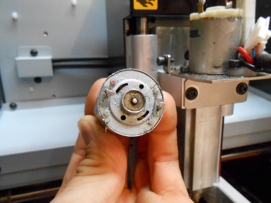
bearing and rotor axis worn out
So I replaced the motor by another one that was lying around in the lab :
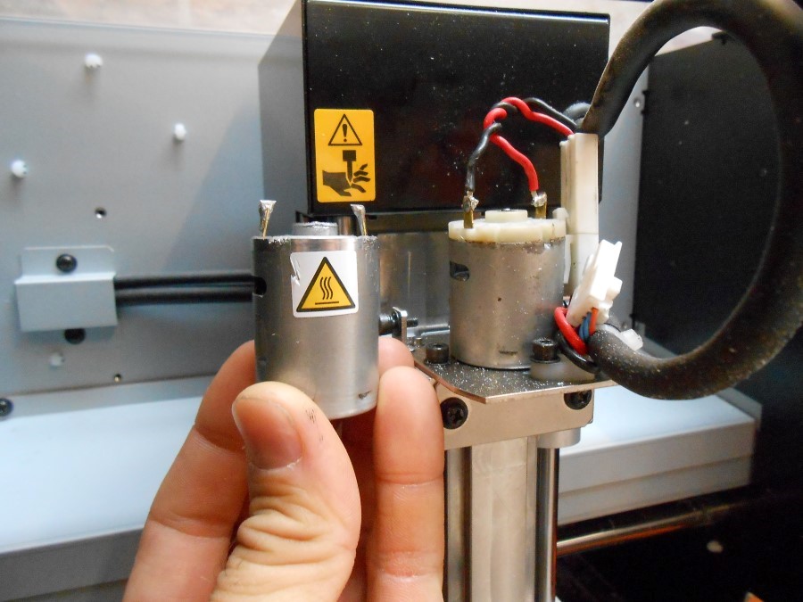
Monofab motor replaced
Only problem is that the new motor doesn't have the same power and the same speed.
So I have to systematically set the speed to 50% of was it usually is :
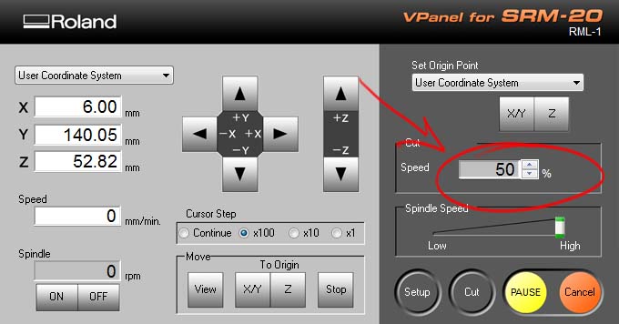
Monofab speed set up at 50%
Aside from this, after all these training weeks, the process was very smooth and quick.
Soldering
Again, it's faster and faster to gather the components and solder them...
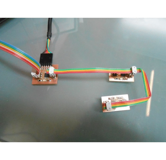
Here are my three boards, populated :
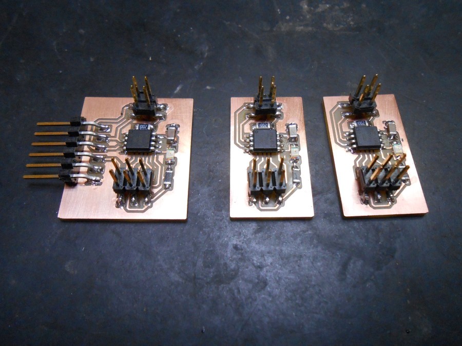
Boards populated
Programming
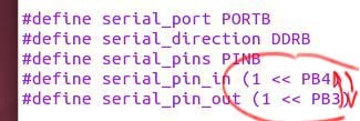
Compare to Neil's design, I have pin 3 and pin 4 inverted, so I need to change that in the code :
Swapping the pins in the C program
I also understood a very simple thing : PB0,1,2,3... are actually predefined names in the avr/io.h header for, well, 1,2,3...
Also, I understood that the PGM_P macro is predefined in the avr/pgmspace.h header and is used to declare a variable that is a pointer to a string in program space.
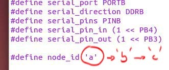
Then, just to believe that I'm original, I change the initial 1,2,3 addressing by a,b,c :
Setting up the addresses
So I have as many firmwares as there are different addresses, here, 3
It seems that I'm experiencing this for the first time but even though my board is working, if I try to use the "burn bootloader" command from the arduino IDE to set the fuses, the microcontroller doesn't respond anymore. It's impossible to communicate with it anymore. Would be glad to know if others are also experiencing this.
I first make sure that the right microcontroller is selected in the Makefile :
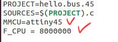
Selecting the right microcontroller
I then compile my C program in a .hex file and upload them to the ATtiny45 with these commands :
sudo make
sudo make program-usbtiny
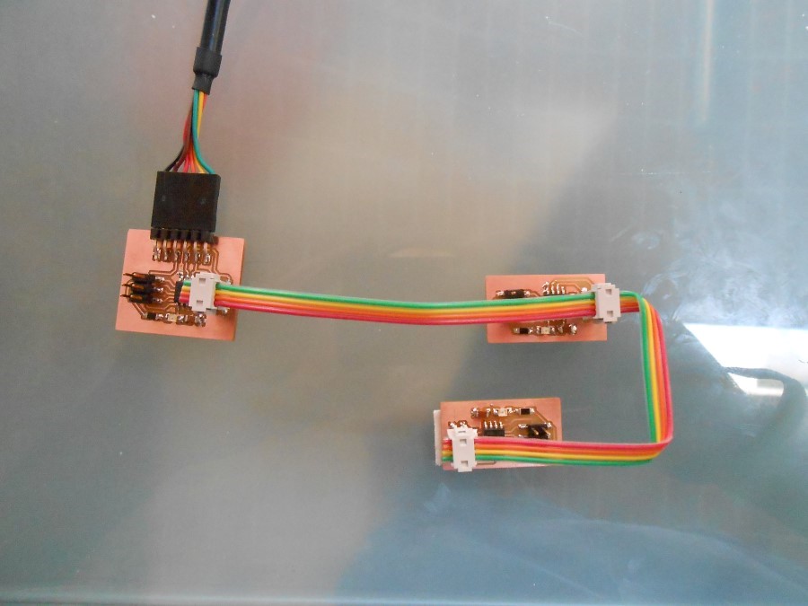
I just have to plug the fabISP serial ribbon cable in each of the board and upload the right (with the right hardcoded address) firmware :
uploading the 3 different firmwares to the boards
Testing
Through the FTDI cable, I'll send addresses and should see the according hardcoded board flash twice.
Network ready to respond
I use term.py to send those serial characters. I start the terminal with this command :
sudo python term.py /dev/ttyUSB0 9600
Here it is in action :
The boards blinking twice when their address is typed
I noticed that when I try to have two programs opening the same serial port on a virtual machine, it can lead to this :
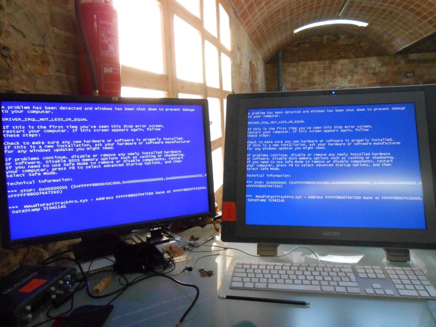
Blue screen of death
Souce Files
Here are the sources files of the projects I talked about on this page :
Bridge board traces PNG for fabmodules.org
Bridge board outline PNG for fabmodules.org
Node board traces PNG for fabmodules.org
Node board outline PNG for fabmodules.org
Bridge board schematic for EAGLE
Bridge board layout for EAGLE
Node board schematic for EAGLE
Node board layout for EAGLE
Conclusion
***