14. Networking and communications
Week 14: Back in the Turbulence. In the early days of the space program Nasa test pilots exit the atmosphere…and are rewarded with a short period of silence in space. But eventually fall back towards earth, pointing straight down and accelerating into the increasingly thick and noisy atmosphere.
The week off was peaceful. I took the time to reflect, assess and plan my Fab Academy journey…and do some light reading to increasing my understanding in areas where I am short of knowledge. The Networking class this week was like a bucket of icy water thrown on my dreamy, Lazy-boy existence…a wake up call to return to reality, join the high speed chase. Once again overwhelmed…time to tighten the seatbelt, grab the control stick, do my best to navigate…and avoid smashing into the ground.
The Assignment:
This week, it’s Networking and Communications. Neil’s lecture was both exciting and incredibly intimidating. The promise of cool things we could do to broaden the capabilities of the standalone devices we have learned to build was joined by rising anxiety of a new area of knowledge that I am sorely lacking.
Individual Assignment: Design, build and connect wired or wireless nodes with network or bus
Group Assignment: Send signals to one another’s devices
The Attack Plan:
- My classmates will individually tackle RS-232 and I2C communication projects
- And I…just to contribute to the breadth of learning in the lab…will tackle a wireless communication project…Bluetooth Low Energy using the RN4871 module (…and if I have time RF using the NRF24OL1)
- The plan…replicate Neil’s boards for those wireless systems, get them to work, try to understand and modify the code to operate them if the first two objectives achieved
Bluetooth Communication - BLE RN4871 2.4GHz Module
BLE - Bluetooth Low Energy
Bluetooth Low Energy is a new concept for bluetooth communication. A great video from Adafruit explaining BLE here
Summary of Adafruit’s explanation of BLE..*
- Uses less energy than traditional Bluetooth devices by keeping things simple
- Doesn’t maintain constant connection (saves energy)
- Sends data on an ‘As Needed’ basis…with little ‘Overhead’
- Good for periodic updates…like getting readings from a sensors
- Not good for streaming audio, video…streaming best for traditional Bluetooth or WIFI
- BLE is low bandwidth
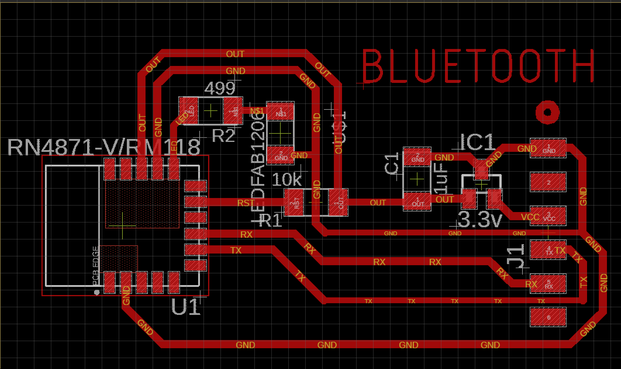
HelloRN4871 Board Production

Parts List
- 1x RN4871 Bluetooth Module
- 1x 10k Resistor
- 1x 1uF Capacitor
- 1x 3.3v Regulator
- 1x 1x6 FTDI Pin Header
I eventually added the following after a 1st failed board version…
- 1x LED
- 1x 499 Resistor
…in order to indicate that the board was ON and functioning
Eagle for Schematic Design and Circuit Board Layout
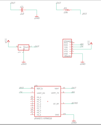
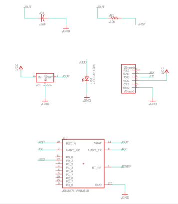
Schematic
With the list of parts created, it is time to work on ‘Schematics’ in Eagle…
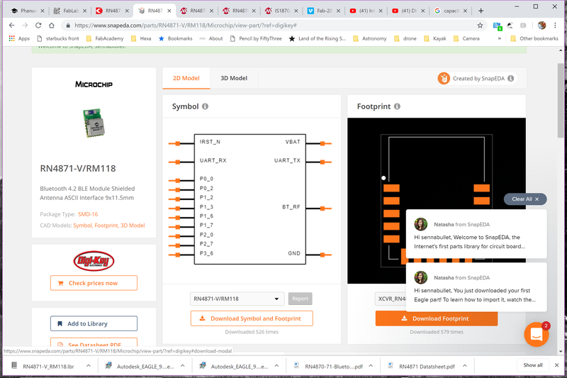
- The Footprint for RN4871 module was not in existing Eagle libraries.
- I Downloaded the footprint for the RN4871 Bluetooth module here…then dragged and dropped the .lbr file into Eagle’s Library Manager
- The schematic diagramming process has become a comfortable routine now…
- I have come to prefer not to draw routing lines directly from one component to another, and create a tangled mess…but rather name the ‘tag end’ of a routing line extending out from one component with the same name as the ‘tag end’ name of the component it is meant to connect to
- I also make sure to add ‘value’ labels to every component (sometimes replacing complicated default values assigned to the component by Eagle) to make them more easily identifiable in the ‘Board Layout’ view…used as reference for stuffing later on
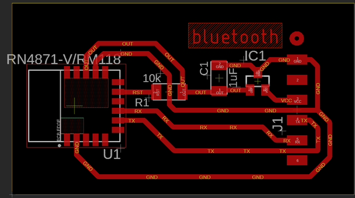
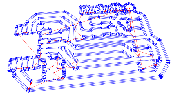
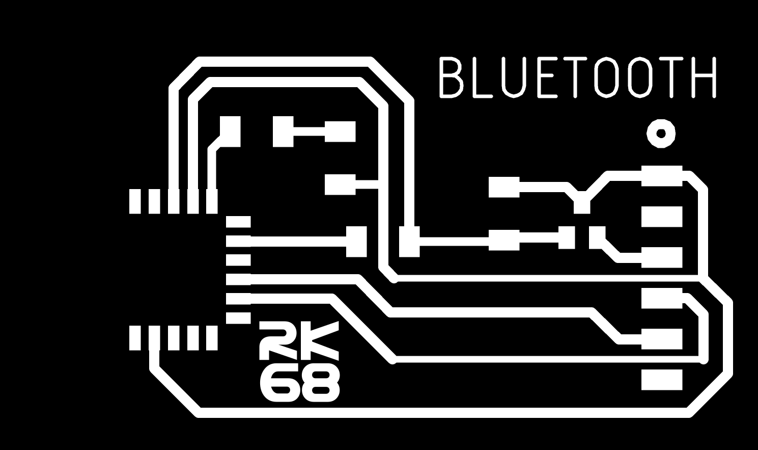
Board (PNG file export)
Schematics done, time to layout the trace lines of the circuit board…
Before proceeding, some settings:
- Grid: Primary grid divisions set at 0.05 in, Finer Secondary grid divisions set to 0.005 in (access using ALT key)
- Design Rules: 15.625mil set for all clearances
Very few components on this board, routing work was not too difficult. In a few instances, trace lines had to be run between pads…so clearances needed to be carefully monitored. Where possible, I chose to make the trace lines as ‘fat’ as possible (0.2) to reduce resistance. Only a couple of the trace lines running between the pads were made narrower (0.16).
After board traces laid out, Trace and Outline PNG files were exported… - monochrome - 800dpi

…ready for RML file converston in Mods.
Adding Decorative Graphics using Inkscape
Before RML conversion in MODs, I decided to decorate my board with graphics (…envious of the work my Shanghai and Seoul colleagues have been doing on their board for weeks!). I used Inkscape for this.
Doing this work, I noticed something strange about the way Inkscape imports PNG files…
- Eagle exported the PNG files at 1406 x 760 pixels @ 800dpi
- Inkscape opens it as 2818 x 1526 pixels @ 800dpi…2x the original size (why?)
-
After adding my graphics and ready for export as new PNG file, these were the steps I took to ensure that the file exported properly and at the right size for RML conversion (discovered after some trial and error)…
- Group: Make sure to ‘Group’ all graphic objects in drawing…in my case, the original PNG image and the added text graphic
- Filename: In the export side menu, specify the save location and filename
- Transform - Scale: This is my workaround for the strange doubling of the image size when I opened in Inkcape. In the ‘Transform’ side menu under the ‘Scale’ tab…I proportionally reduced the selected grouped graphic by 50%
- Export: With the preceding steps completed…I clicked the ‘Export’ button (with the green check mark) in the export side menu to generate the new, decorated, PNG file

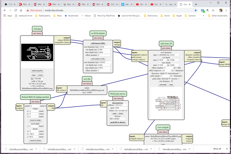
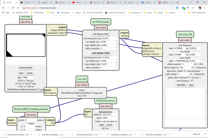
Convert PNG to RML File in MODs
Preparing MODs for conversion work: 1. Right mouse click, choose…Programs > Open Server Program > SRM-20 > PCB PNG 2. In the ‘SRM-20 Milling Machine’ module (lower left of screen)…set X,Y,Z ‘Origin’ to zero 3. In the empty space next to the ‘SRM-20 Milling Machine’ module, right mouse click, choose…Modules > Open Server Modules > File > Save…(this step is necessary in the Kamakura lab because our SRM-20 machine is not connected to the network)
Converting PNG file to RML file 1. Import the saved PNG files one by one…double check once again that the DPI and size of the board (in Pixels, or mm, or inches) is consistent with the size of the board exported from Eagle - In ‘Set PCB Defaults’…click ‘Mill Traces 1/64’ for TRACE PNG file (note that Tool Diameter is 0.0156in, Cut Depth and Max Depth are 0.004in, and Offset Number is 4)....click ‘Mill Outline 1/32’ for OUTLINE PNG file (note that Tool Diameter is 0.0312in, Cut Depth and Max Depth are 0.024in and 0.072, and Offset Number is 1) - In ‘Mill Raster 2D’…click ‘Calculate’ to generate 2D and 3D tool path and save RML files…a pop up window with the 3D tool path image should appear (simultaneously, an RML file is generated and saved to the ‘Downloads’ folder)…check toolpath carefully to ensure that tool path lines run between all pads and traces, that unintended bridging between trace lines and pads will not occur…if bridging occurred, 2 options to fix - Go back to Eagle to create greater clearances at problematic areas…this is the most correct method - In the ‘Set PCB Defaults’ reduce the ‘Tool Diameter’ from default 0.0156 to something smaller…this is a ‘cheat’ and may result in problems if the width is reduced too much…from personal experience, reduction to 0.0149 seems to be OK.

Milling
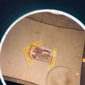
Pretty straight forward. Milling the PCB was successful with no issues arising.
Stuffing

Not only have I come to appreciate creating a physical components list next to which I tape the actual components…and make notes below with regards to key pins from the primary component that I need to focus on…from this week, I have decided to keep these lists in a notebook. In the past, I discovered that if I kept this piece of paper, it made making subsequent boards that much easier. So rather than having loose pieces of paper (that I will eventually lose) I will keep this component lists safely in a notebook.
Soldering the few components on to the board was mostly simple…the RN4871 BLE module proving a little difficult. The components doesn’t have legs at pin locations, but instead has notches aligning to pin traces. A bit of patience, some liquid flux, a very fine soldering tip and 0.3mm solder…and the module was successfully soldered on.
First Board: FAIL!
Plugged the board in, not certain if it was on. Installed a BLE Scanner app into my Android phone, scanned for BLE devices, plugged and unplugged the board to the FTDI cable for power…the board did not appear.
With the board powered by the FTDI cable, I used a multimeter to check voltages around the board. The voltage at the FTDI VCC is 5.0v…but strangely, the voltage out of the Regulator was 4.13v…not the expected 3.3v. Turned out I used the wrong Regulator. The 5.0v regulator (which I used…is labeled L0B on top) is VERY similar in size and appearance to the 3.3v regulator (labeled L0A on top).
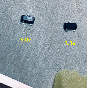 …these components are tiny and nearly indistinguishable. Even their ‘Item Code’ is very similar. But be mindful to read the package info the next time!
I tried desoldering the incorrect regulator off the board and soldering on the correct one, but this still did not make the board identifiable by the BLE scanner…I assumed that I burned out the BLE module with too much voltage. I decided to build another board.
Second Board: Success!
I milled and stuffed a second board, this time with the correct regulator. I also added an LED (connected to pin P0/2 in accordance with datasheet specifications) to help me know when the board is powered an ON (made adjustments to the circuit design in Eagle, adding an LED and 499 ohm resister).
LED added, connected to pin P0/2


…cheated a bit on the 1/64” mill diameter specification, reducing the number from 0.0156 to 0.015…to eliminate pad/trace bridging and tool paths to be defined between them.


When completed, I powered the board via the FTDI cable and…success!!! The green LED lights and blinks. The BLE Scanner recognizes the device.
Bluetooth Communications
The board is operational and recognized by the bluetoooth scanner. Now it’s time to get it communicating.
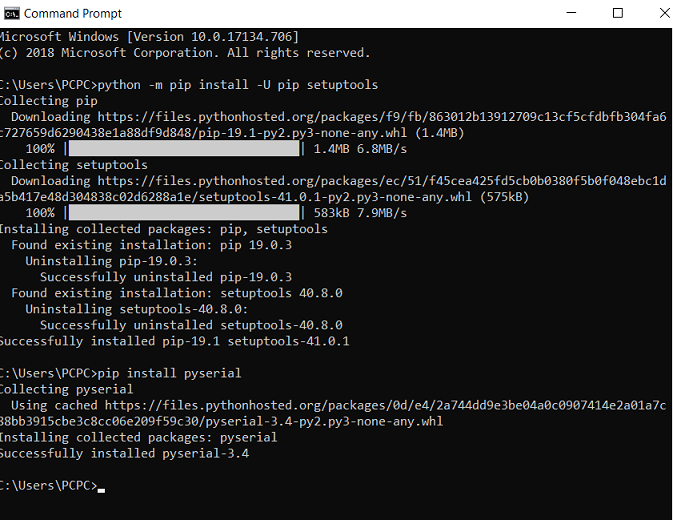
To do that, I followed instructions provided by JakNil to install Python and the required Serial Library here
Then following the excellent documentation of Joris Navarro here…and after a ton of complicated setup of the HelloRN4871Bluetooth Board” on Python Miniterm in the laptop
- To communicate via an FTDI cable out of port COM4 at a baud rate of 115200 Settings:
- Type ‘$$$’…to get ‘CMD>’
- Type ‘+’…to turn Echo ON
- Type ‘ss,c0’…to set Support Device Info and UART Transparent services as Default services
- Type ‘R,1’…to reboot the terminal and lock in settings just made
The chip is now in UART transparent mode…allowing the chip’s RX will be sent to the TX of the serial console (according to Joris, I don’t quite understand this…yet)
And with the installation and setup of the Nordic nRF Connect App for Android
- Connecting to my Bluetooth board…with the ID ‘BLE-FCF1’
- Selecting ‘Unknown Services’ and ‘Unknown Characteristics’
- Turning on ‘Notification’ (and disable ‘Indications’) by clicking on the ‘3 Down Arrows’ icon
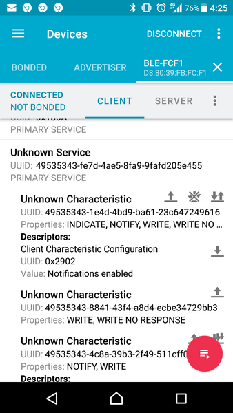
I was able to send messages back and forth between my mobile phone and the Windows laptop.

In the mobile phone app…I typed “hello fabworld”
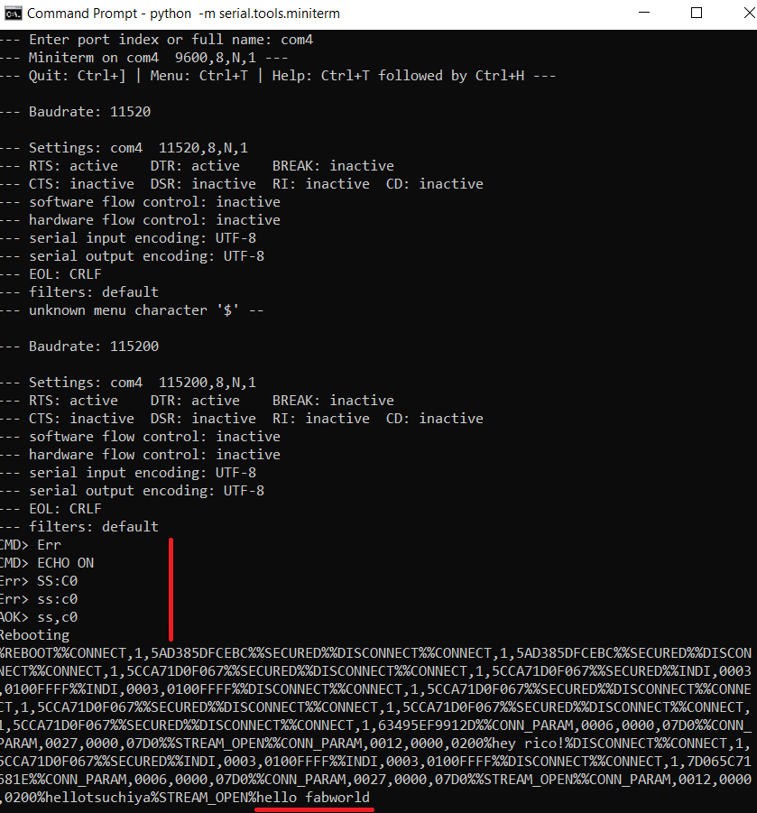
And magically, “hello fabworld” appeared in the laptop terminal console.
Interestingly, I was only able to send a single character at a time from the laptop to the mobile phone…but was able to write a full string from the mobile to the laptop.
Addendum: in Joris’ notes, he mentions that if I type…only a single character at a time will be sent…but if I paste a whole string will be sent
Another Mistake
At the week 15 lecture, Neil points out to those of us doing wireless radio boards…not to have the PCB copper under the antennae. I remembered when looking at Neil’s example board saying to myself “Why did he have the Bluetooth module sticking past the edge of the board? Seems like it would make it vulnerable to being broken off.” And consequently I left PCB material under the bluetooth module, as protection. During the lecture, Neil informs us electronics noobs that doing so interferes/dampens the radio signal from the module. Duh…no wonder there were so few signal bars generated by the board when I scanned for it!
Surgery time.

Strapped down the board and took a dremel to it.

Managed to get the excess PCB under the antennae cut off without damaging the bluetooth module (I think).

Powered up the board and scanned for it using my mobile phone. It appeared!!!…and with a stronger signal than before (probably 2 bars max previously). Whew!
Files
<<<<<<< HEAD - The Schematic file for my board is here - The Board Layout file for my board is here - The board Trace .PNG File is here - The board Outline .PNG File is here - The board Trace .RML File is here - The board Outline .RML File is here
Files
- The Schematic file for my board is here
- The Board Layout file for my board is here
- The board Trace .PNG File is here
- The board Outline .PNG File is here
- The board Trace .RML File is here
- The board Outline .RML File is here
Appendix
UART
- Universal Asynchronous Receiver Transmitter
- Serial communication
- 2 devices communicating data back and forth…binary
- Wired connection