Electronics design
Assignment for this week
- Redraw the echo hello-world board
- Add (at least) a button and LED (with current-limiting resistor)
- Check the design rules, and make it
- Link to this week’s home work page
This week's lecture was about electronics design and electronic design tools. We reviewed the most common electronic components (wires, switches, resistors, capacitors, resonators, diodes, transistors (MOSFETs), ... the microcontrollers and the sensors and actuators will be discussed later) and their main functions. Then we went very briefly through the list of the most common electronics design tools and as usual at the FabAcademy, students will have to learn by themselves by exploring the various available softwares. EagleCAD was pointed out as a very powerfull tool to go from schematics to board layouts (although not open source, the evaluation version is fully functional but limited to 160mmx100mm). Looking at the student archive it is certainly the most used. KiCAD is an excellent open source alternative that can in addition render the boards in 3d which may be useful if one wants to import the board in a CAD design tool.
This page is organized as follows:
- The objective
- Workflow in EagleCAD
- Workflow in KiCAD
- Milling the board with FabModule and Roland modela MDX40
- Soldering the components
The objective

Workflow in EagleCAD
I installed EagleCAD 7.5 on my Macbook Pro. Many tutorials can be found on the web, I recommend this one for schematics and the part 2 for board layout. I downloaded the fab library that contain the schamtics and the footprints of the electronic components used in the FabAcademy program. I put the fab.lbr file in the main EagleCAD libary folder /Applications/EAGLE-7.5.0/lbr/ so that it can be accessible without having to specify a given directory.
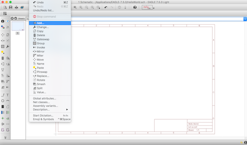
The first thing to do is to create a new project (File>New>Project) and then within the newly created project create a new Schematic (File>New>Schematic). Then select and add the components using Edit>Add.... You can end the process with ESC.

The list of components to be added was the following:
- 6MM_SWITCH6MM_SWITCH
- ATTINY44>ATTINY44-SSU
- AVRISP>AVRISPMD (J1-ISP)
- CAP-US> CAP-US1206FAB (C1-1uF)
- FDTI-SMD-HEADER (J2-FTDI)
- LED>LEDFAB1206 (LED1206)
- RES-US>RES-US1206FAB (R1 10k)
- RESONATOR (XTAL 1 - 20MHZ - EFOBM)
One then needs to find a proper place for the components and then add wires between the components. I used the net tool  not the wire tool
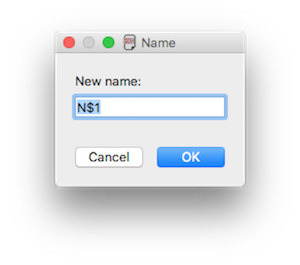
  . To avoid wires everywhere, I decided to name the nets and to connect the nets using the net names. I first added a small segment of wire to each pins (terminate the wire with ESC), then used the name tool
  (beware of using the name tool on the left and not the value tool which has the same icon but is on the right side of the toolbar) and click on the segment. A pop up windo appears asking for a new net name.
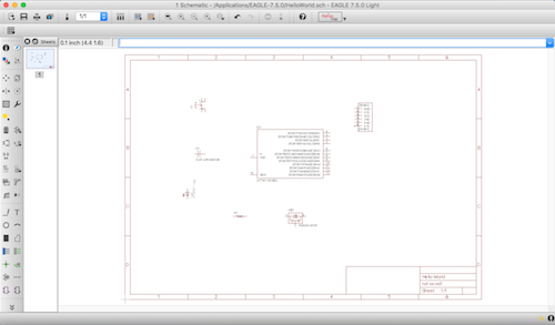
Then, in order to make the net names visible on the schematic, I used the label tool  . With this tool active, a click on a named net makes the name visible. Using this net naming process, it is rather easy to connect IC pins to connector pins. In the end, I obtained this schematic which features 2 LEDs and a button.
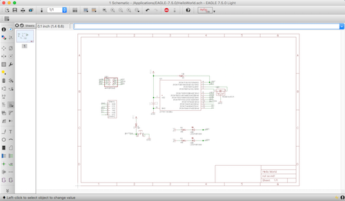
At this stage, it is necessary to check the schematic (Tools>ERC). Very often the ERC check reavealed connection problems. To solve them, just move the component a little bit (select the Move tool  and click on the component, it should turn bright red) to see if the wires move with it as they should. If not reconnect the components. Once the schematic passes the ERC check it is possible to switch to board layout (File>Switch to board).
Board layout
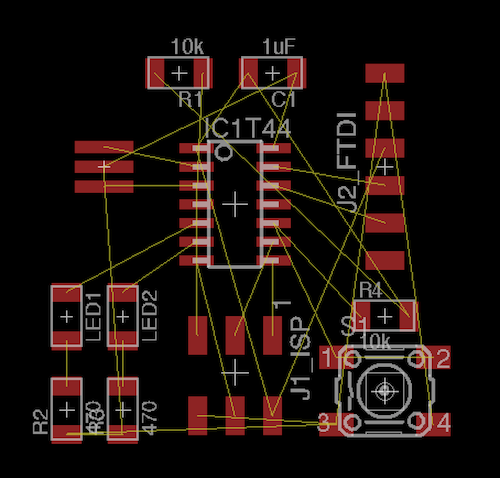
At first, all the components are packed on the left of the page with yellow lines showing the connections between them. I move them (use the Group tool  to select all the components by drawing a square around them and then right click > Move) to the center of the page and started to find a good place for them (trying to avoid connection lines crossings ansd tring to the original design provided during the class. Using the Move tool, it is possible to rotate the component with a right click.
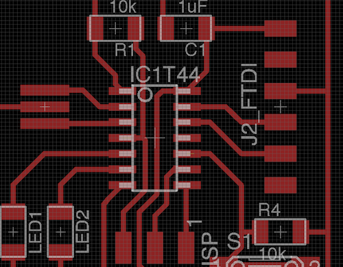
After cleaning,
Now, it's time to add traces and connect components using the Route tool  . I used the grid (0.025'') and the wire bend style 1 and a track width of 0.016''.

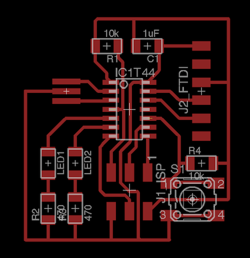
At this stage, things become more complicated, because on the traces provided in class we see that 3 traces must pass below the ATTiny44 chip.
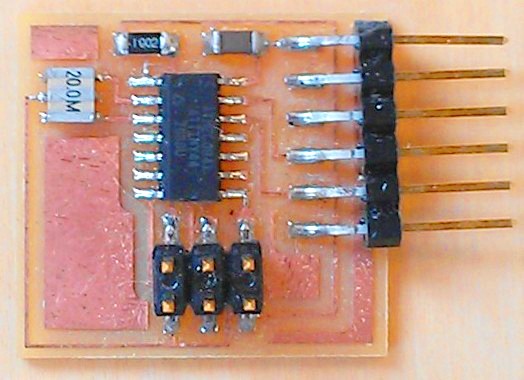
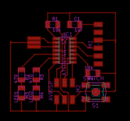
I reduced the grid size (0.0125'' and alt 0.00625'') to position the tracks more precisely. Finally, the board I obtained looked like this:
Workflow in KiCAD
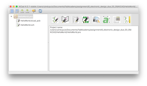
I installed KiCAD 4.0.1 on my Macbook Pro. I like KiCAD because it's open source and it can render 3d view of the board with the components (for in EagleCAD you have to pay). Moreover you can control almost everything from the keyboard with hotkeys. During the week, we received several emails regarding the port of the fab library to KiCAD. I download the libaries here. I created a new project HelloWorld and this generates 3 files in the project folder: HelloWorld.pro, HelloWorld.sch and HelloWorld.kicad_pcb.
The schematic editor in KiCAD is named Eeschema (first icon from the left on the start window). Before adding components, I imported the fab libraries (Preferences>Component libraries>Add on the right side of the Component libary files after selecting the project folder path). It is local possible ot use a relative path. Strangely enough, I found that there was a scale problem when I used libaries in subfolders. I solved this by putting the lib and mod file right in the project root directory.

To add a component, just type a, ESC to end the process.
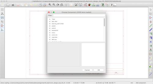
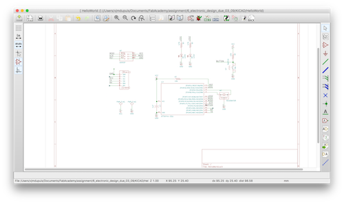
I then added the components and placed them in a similar way as I did in EagleCAD. I used m to move, r to rotate components, w to connect components (it is possible to end a track using k). I used the net name tool  to name the IC and connector pins and thus create connections between them (I could have used l). I also added Power Flags connection to Vcc and GND as recommended in various tutorials.
Once the schematic is drawn, I performed an electrical rule check (ERC  ) and then generated the Net list
  .
.
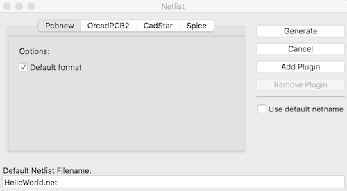
During the process, KiCAD performs an annotation of the components and eventually creates a file HelloWorld.net. A this stage it is necessary to associate components and footprints. This is done by clicking on CvPCB  .
.

It is necessary to specify the footprint library path in Preferences>Footprint libraries.
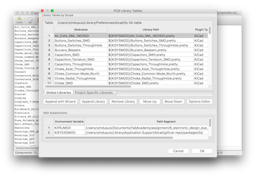
I used Append with Wizard>Files on my local computer and specified the fab.mod file in the project root directory.

Once done, when you click on the components in the list in the middle pane, a footprint suggestion appears in the right pane. The association is done by clicking on the footprint name in the right pane. Once the association is finished, there should be the 0 unassigned components indication at the bottom of the CvPCB window. Save and exit.

It's now possible to start the board layout by runing PCBnew  . A blanck black page appears. To import the footprints it is nessary to click on the Read NetList icon
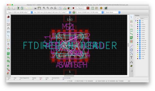
  and then click Read Current NetList. All the footprint are initially packed in the center of the page.
To separate the footprints, click on the Mode footprint icon  . Then draw a square around the components, right click and Global Spread and Place > Spread out All Footprints.
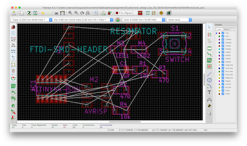
After cleaning at bit,
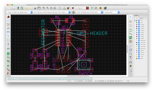
Time to route. To change the track width, one must go to Design Rules > Design rules > Click on the Global Design Rules pane and add values in the cells of the Custom Track Widths table (bottom right). I added 0.016'' in the track width list to be consistent with what I did with EagleCAD. To add tracks, select the Track and Vias tools  and connect components. At the end of each track, right click and select End Track to validate the track.
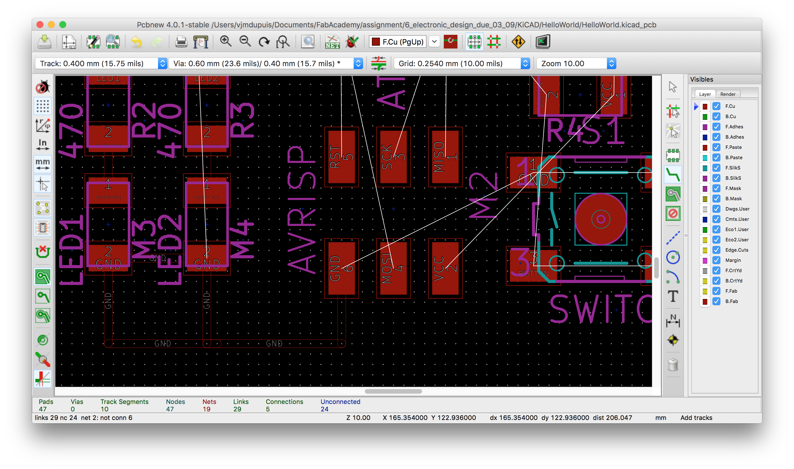
What is nice with KiCAD is that you can see the netnames on the pads while routing.

Done !

And finally, the 3d view:
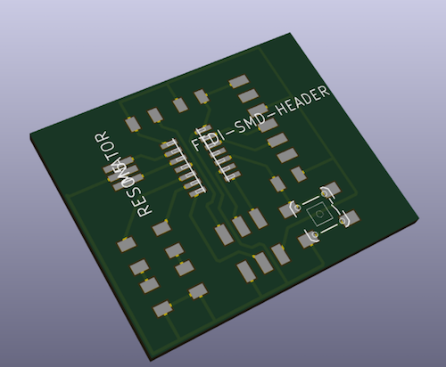
Of course, it would be better with the components in 3d but they are not yet implemented in the fab kicad library.
Changing the components to adapt our instructor's order mistake
Unfortunately, our instructor made a mistake when ordering the components from digikeys.
| Quantity | Reference | Reference Fab. | Description | Unit price | Total price |
| 5 | 73-1001- ND | 506 | PCB COPPER CLAD 4X6 1/16" 1-SIDE | 5,43000 | 27,15 € |
| 15 | ATTINY44A- SSU-ND | ATTINY44A-SSU | IC MCU 8BIT 4KB FLASH 14SOIC | 1,19900 | 17,99 € |
| 15 | 644-1039-1- ND | NX5032GA-20.000000MHZ-LN-CD-1 | CRYSTAL 20.0000MHZ 8PF SMD | 0,46300 | 6,95 € |
| 15 | H2961CT- ND | UX60A-MB-5ST | CONN RECEPT MINI USB2.0 5POS | 0,81600 | 12,24 € |
| 15 | 609-3693-1- ND | 20021121-00006C4LF | CONN HEADER 6POS DL UNSHRD SMD | 0,43600 | 6,54 € |
| 50 | 490-6186-1- ND | GRM1555C1H100FA01D | CAP CER 10PF 50V NP0 0402 | 0,02060 | 1,03 € |
| 50 | 490-1320-1- ND | GRM155R60J105KE19D | CAP CER 1UF 6.3V X5R0402 | 0,02620 | 1,31 € |
| 50 | BZT52C3V3- FDICT-ND | BZT52C3V3-7-F | DIODE ZENER 3.3V 500MW SOD123 | 0,16600 | 8,30 € |
| 50 | 311- 1.0KGRCT- ND | RC0603JR-071KL | RES SMD 1K OHM 5% 1/10W 0603 | 0,00720 | 0,36 € |
| 50 | 311- 499LRCT- ND | RC0402FR-07499RL | RES SMD 499 OHM 1% 1/16W 0402 | 0,00840 | 0,42 € |
| 50 | 311- 100LRCT- ND | RC0402FR-07100RL | RES SMD 100 OHM 1% 1/16W 0402 | 0,00840 | 0,42 € |
| 50 | 10KJRCT- ND | RC0402JR-0710KL | RES SMD 10K OHM 5% 1/16W 0402 | 0,00720 | 0,36 € |
| 50 | 311- 0.0GRCT- ND | RC0603JR-070RL | RES SMD 0.0OHM JUMPER 1/10W 0603 | 0,00720 | 0,36 € |
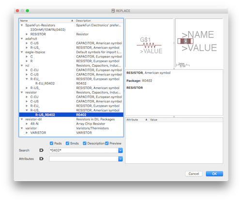
The mistake is clear, instead of 0603 SMD resistors and caps, the ordered ones have a 0402 package except for the 1k resistor and the jumper. This means I have to replace the wrong components by their equivalent with 0402 packages. I used EagleCAD. I created a new projet HelloWorld2 and copied the HelloWorld1 sch and brd file in it. After renaming them HelloWorld2.sch and HelloWorld2.brd, I opened HelloWorld2.sch in the HelloWorld2 EagleCAD project. The switch to board brought the HelloWorld2.brd so the association between the two renamed files worked. I right clicked on the 0603 components and used the Replace tool 
Eagle automatically modifies the board to take into account the change and adjust the traces.

Of course, soldering 0402 is not goind to be as easy as sodering 0603 components.
Milling the board with FabModule and Roland modela MDX40
To mill the board, I exported the .brd file to png and cropped it (using mac os x preview ) and created et contour using Gimp (import png, create a square zone that contains the traces and clear). The CNC at Fablab Digiscope is a Roland modela MDX40.
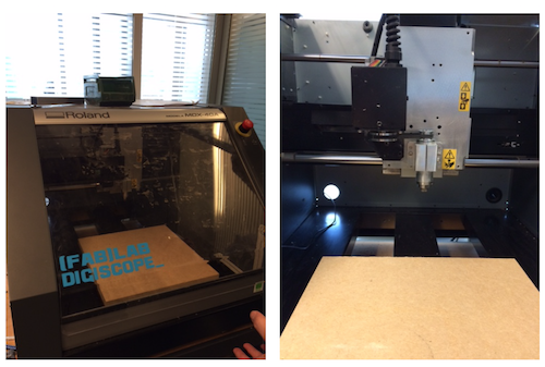
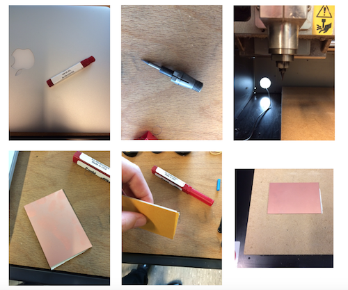
I first installed the 1/64'' (0.4mm) drill that will be used to mill the PCB and fixed the the FR1 laminate (thickness = 1.7 mm) with double sided tape on the MDX40 wood plateau.
I then used the Fab Modules and imported the HelloWorld.png.
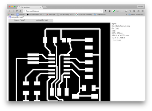
I chose rml in the output format list.

I then selected PCB traces 1/64 because I will be using a 1/64'' drill for traces 0.4mm wide. I set 15000 mm/s for the speed. The choice of the 1/64'' sets several parameters to some predefined values (tool diameter = 0.4 mm, cut depth = 0.1 mm, number of offsets = 4 (number of passes), offset overlap = 50%.)

Finally, I clicked on the 'caclulate' button to ask FabModules to calculate the tool path (black lines, red lines correspond to transport steps of the tool).
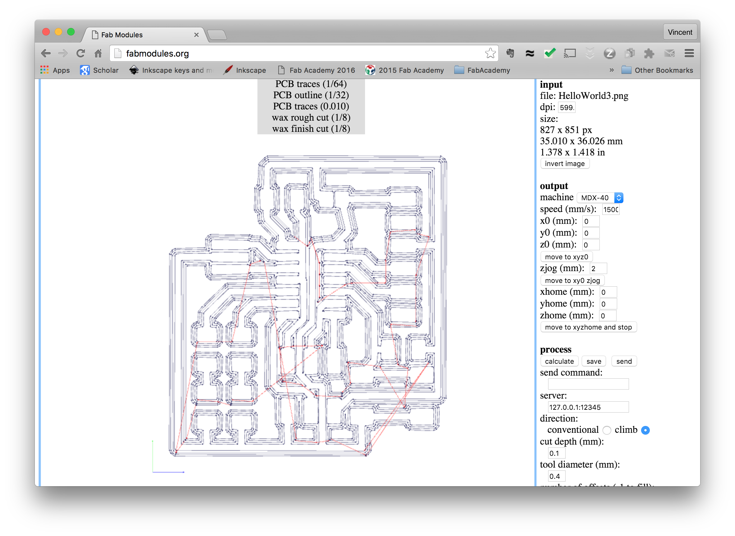
I finished by clicking on the 'save' button to produce a .rml file that I copied on a usb flash drive and plugged the flash drive on the PC so that it could be opened by VPanel the Roland MDX40 software. Before starting the milling, the operator has to set the XYZ origin, the Z origin being the most delicate setting.

The XYZ origin can be aduster by clicking on the red, green and blue arrows respectively. Different speeds can be used (high, low, 100, 10 and 1 Steps, 1 step is 10 um). I adjusted the drill speed to 15000 rpm but set the cutting speed to 10%. To set the Z origin, I made a slow approch towoard the FR1 laminates with the drill rotating (to avoid breaking the drill in case of strong contact with the laminate). When the tip touches the surface of the FR1 laminate, some chips are clearly visible. I then clicked on the 'Apply' button on the right of Set XYZ Origin. Another technique consist in unmounting the drill (with the rotation turned off) and letting it fall onto the surface of the laminate from a height of 1-2 mm, then will 1 or 2 10um steps, the chips are visible and the Z Origin can be set. Once everyhing is set, the milling process begins by clicking on the 'Cut...' button and selecting the proper .rml file.
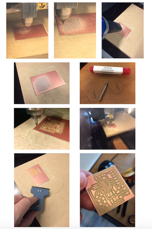
The process is repeated with the 1/32'' drill and the contour .rml file resulting from processing the contour png file with the FabModules (some parameters are changed such as the number of offsets that is set to 1). Once done (Quit cutting) pushing the button 'View' on the MDX40 moves the plateau towards the operature and the board can be removed.
Soldering the components
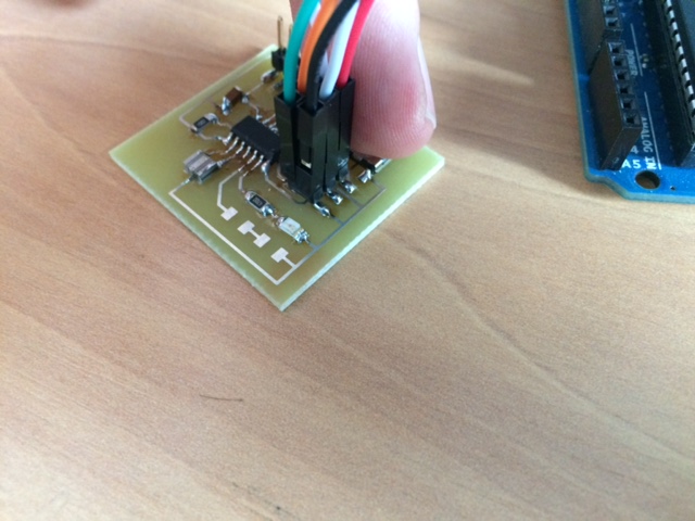
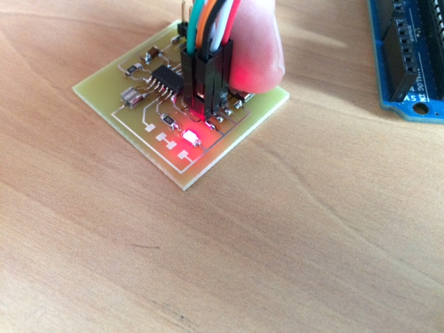
I still don't have all the component, in particular the LEDs and the button but I started to solder the ATTiny.
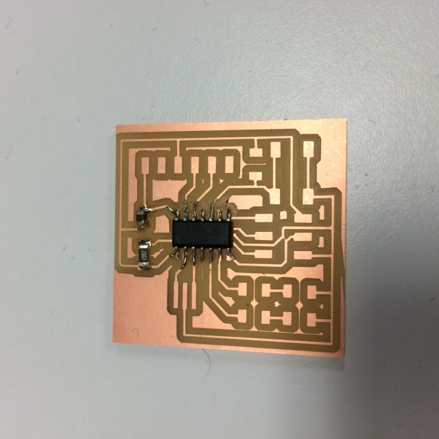
Later, the components arrived but the first prototype did not work. I etched a second board and soldered the component and could programm it (see Embedded programming).
Firmware upload succeeded and finally I could command the LED with the button.