
Electronics Design
To fulfill the assignment I decided to use Eagle to design the board. And for fabrication I used Rolland MDX40A machine along with fab modules to control it.
Current Limiting Resistor
Checking the datasheet of the microcontroller I found out that at VCC= 5v the voltage of the outpins is 4.3 V and the current is 10.0 mA and it can go up to 40.0 mA/ pin. Since Voltage is equal to current * resistance then the R=V/I. Current Limiting Resistor= 4.3/10mA= 430 ohm.
I used 499 ohm resistor as it's much easier to find and it's close enough.
Designing
First step was to check the datasheet for the microcontroller to know the connections so I could draw the Schematic.

Here are the things I decided to include in my design:
-Two input capacitors across VCC and GND to have more stable supply
-LED with current limiting resistor to indicate power On
-LED as an output of one of the digital pins of the Microcontroller
-A crystal with its capacitors to have better time precision
-Pins for all the pins of the microcontroller
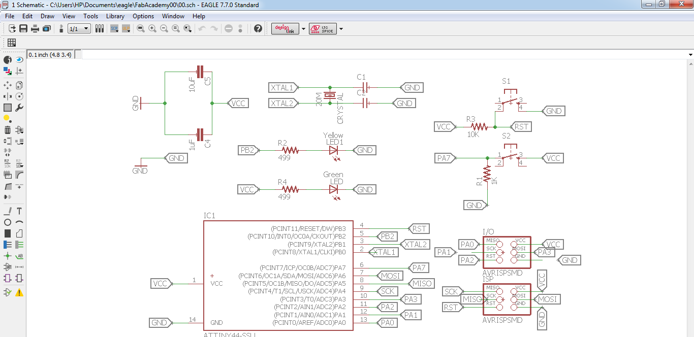
Schematic:
In this section I will be listing all the commands I used to draw the schematic.
-But before starting to draw the schematic I created a new project and then a new a new schematic by going to File-->New-->Project. Then I right clicked the project and clicked -->New-->Schematic.


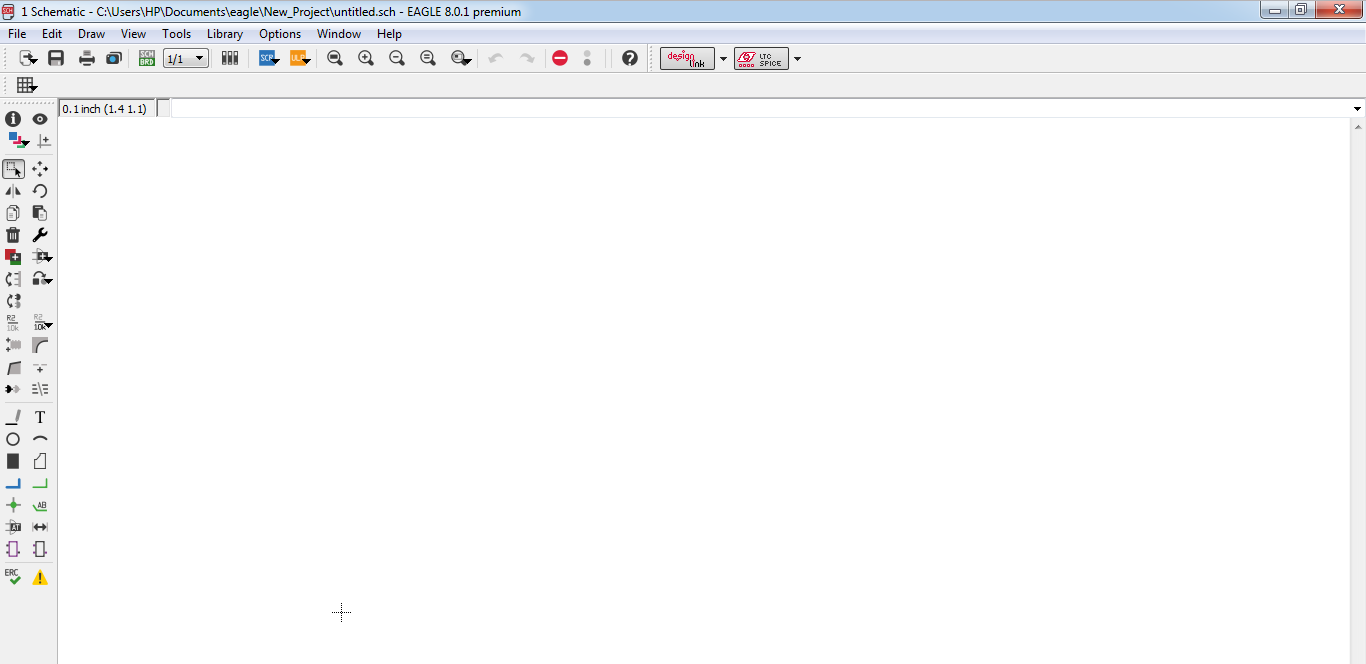
-This is how the working space of the schematic looks like.
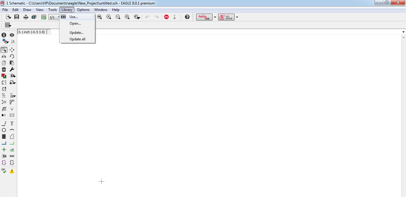
-I started by adding the library of the componenets that I needed I downloaded the .lib file from FabAcademy archive. Then clicked on -->library-->Use.Finally I selected the file and clicked Open

-Next thing I did was to add the components. I clicked on Add tool in the tool bar on the left side of the screen. I scrolled down to fab library expanded it and chose ATiny 44 with package of SOIC14.

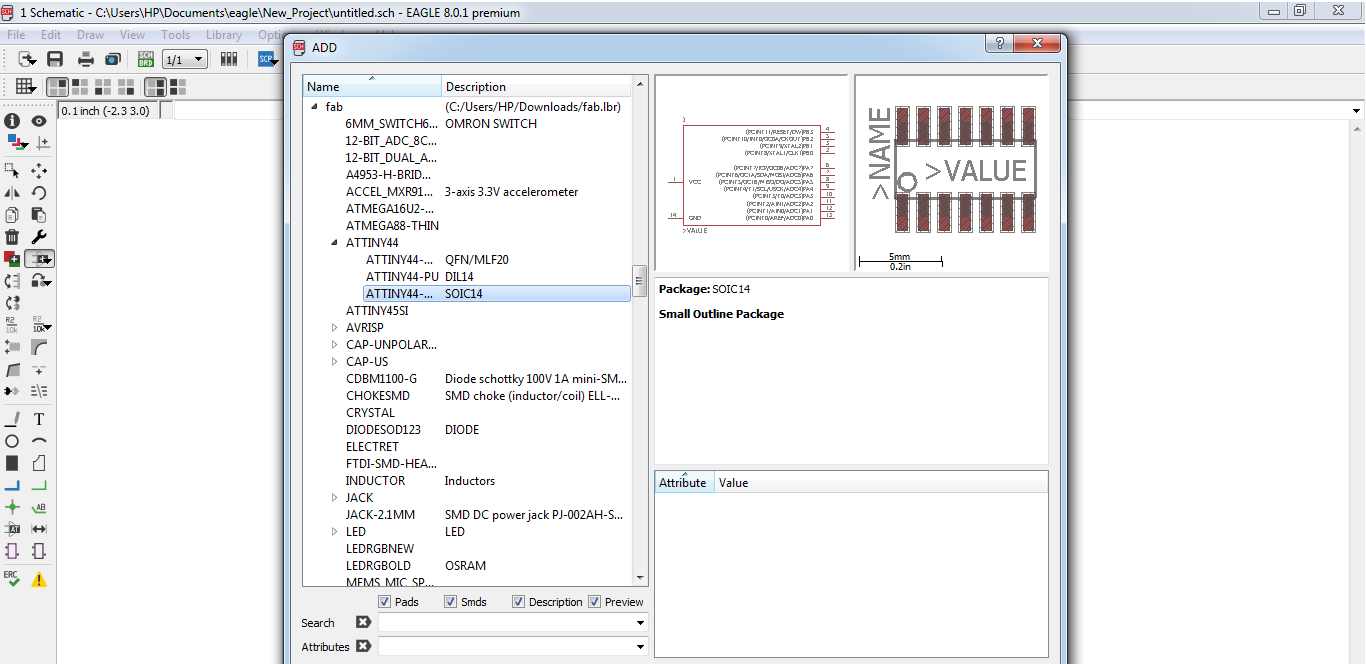
-Finally I pressed Ok and placed it.

-After placing the microcontroller I pressed ESC and went back to the add menu and I added the following components from their libraries:
GND-->Supply1
VCC-->Supply1
6MM_SWITCH-->fab
Capacitor 1206-->fab-->Cap-Unpolarized1206
Led -->fab-->Led 1206
Resistance-->fab-->RES-US1206
20 MHZ Crystal-->fab-->Crystal 2-SMD-5X3MM
SMD Pinheaders-->fab-->AVRISP-->AVRISP 2*03SMD
-To move a component. I chose the move tool from the tool bar, selected the component from its cross and moved it. Other way would be to right click the component and chossing move.

-To change the name of a component I right clicked it and chose Name.
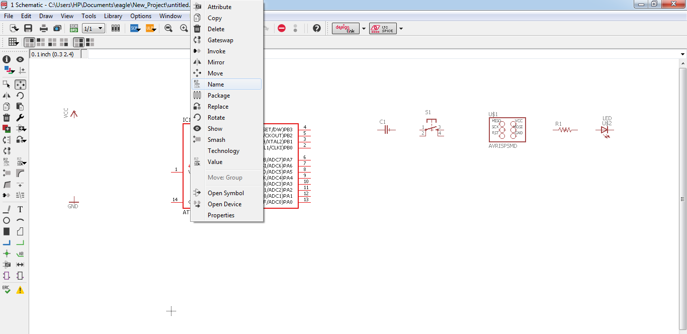
-To change the value of a component. I chose the Value tool from the tool bar, selected the component from its cross and entered the correct value. Other way would be to right click the component and chossing value.

-To copy a component. I chose the Copy tool from the tool bar, selected the component from its cross and placed the copy where I wanted.

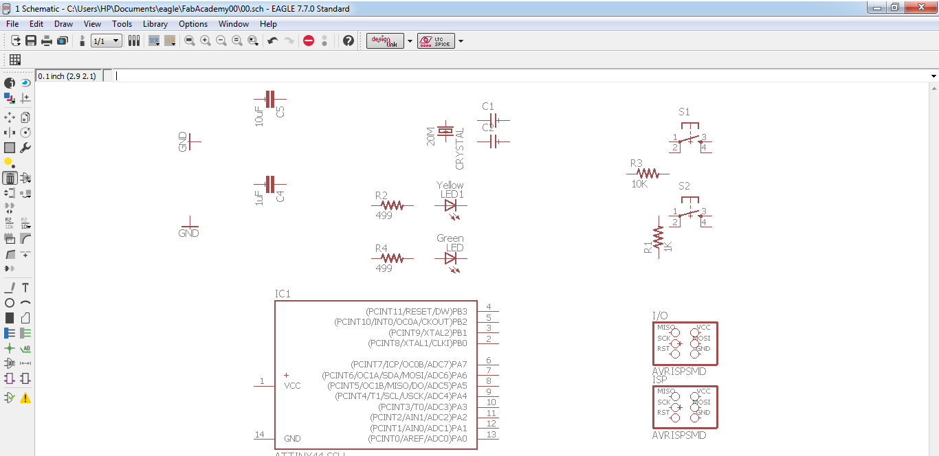
-I kept using those commands until I reached the stage of having all the components of the correct Values and more or less placement.
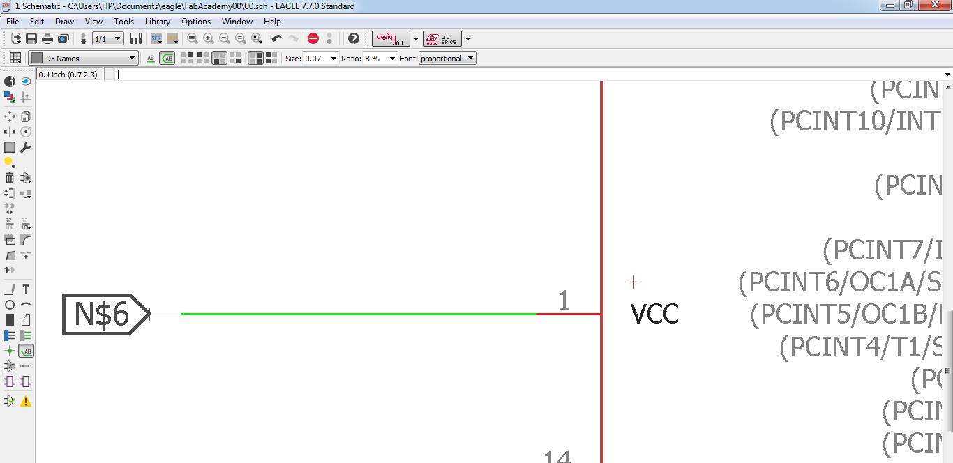
-To connect the components I used the Net command from the tool bar. As some of the components were far from others they should be connected to it's not wise to use only the Net.

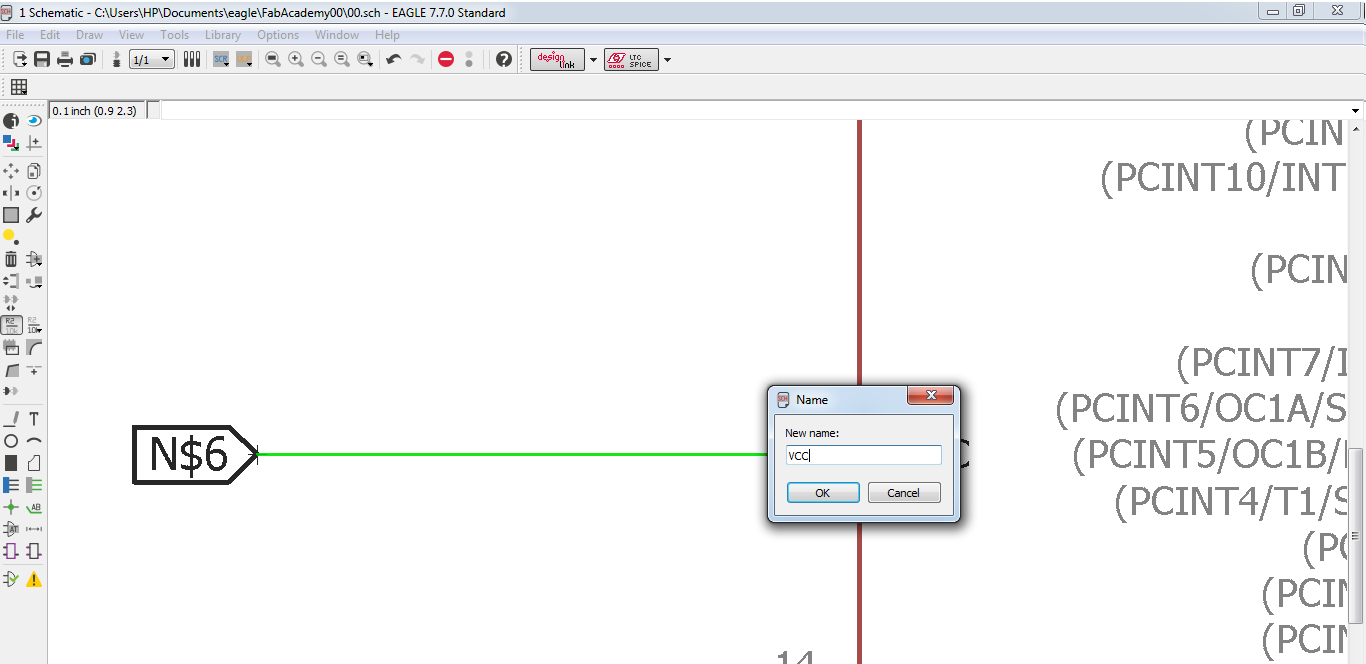
-I used Label tool along with the Net. The idea is to connect a small wire using net to one node and to the same thing to the other node to be connected to it and add a label to both of them with the same name using the name tool
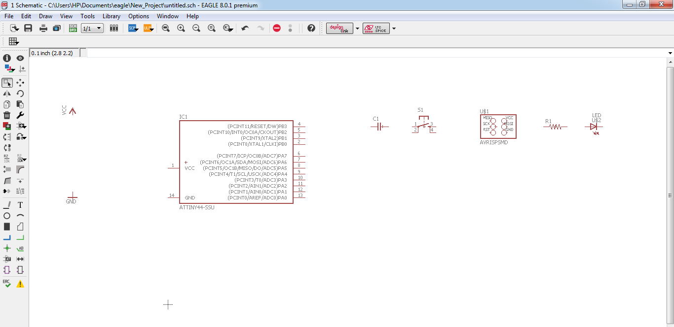
-I used the same strategy to connect everything and this is how it finally looked like.
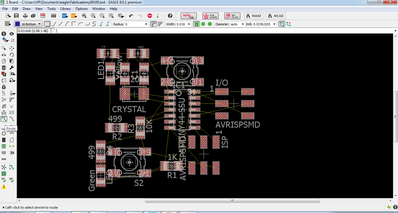
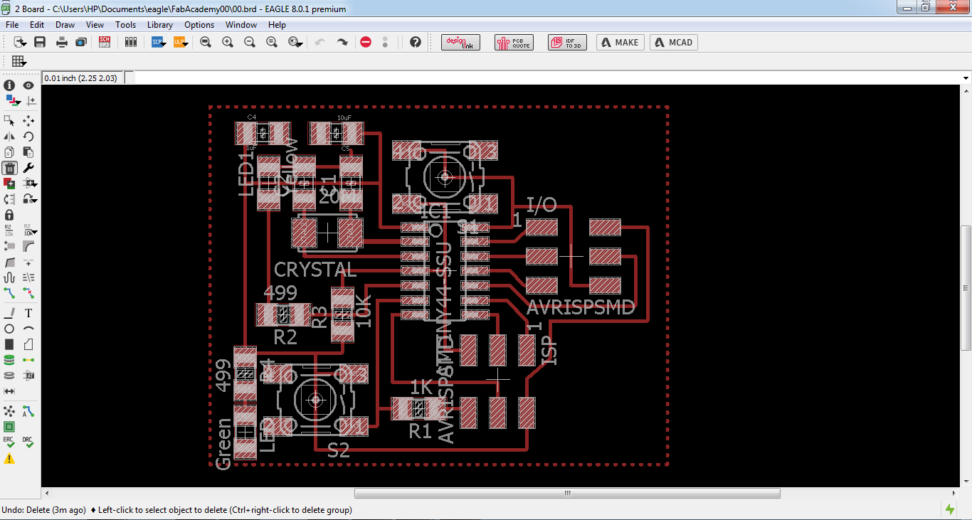
Routing:
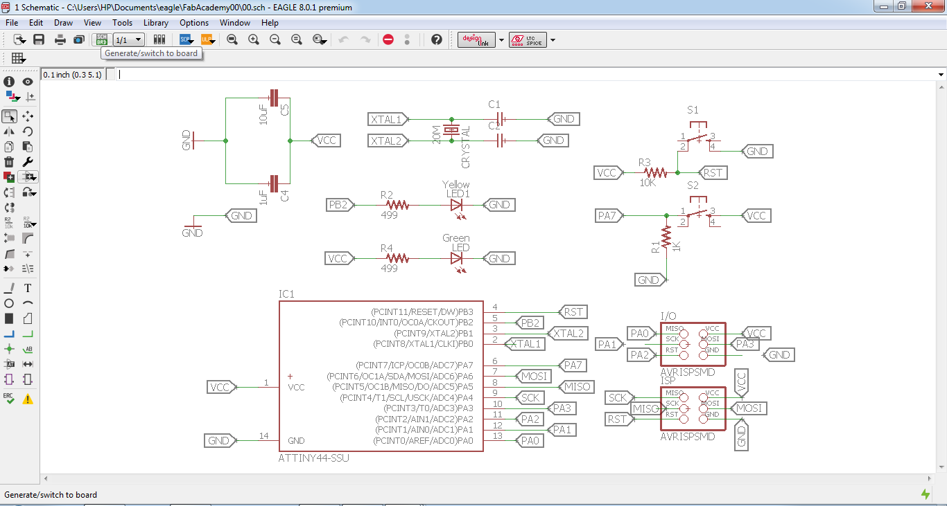
-First step was to generate the board from the schematic by pessing on Switch To Board Button.

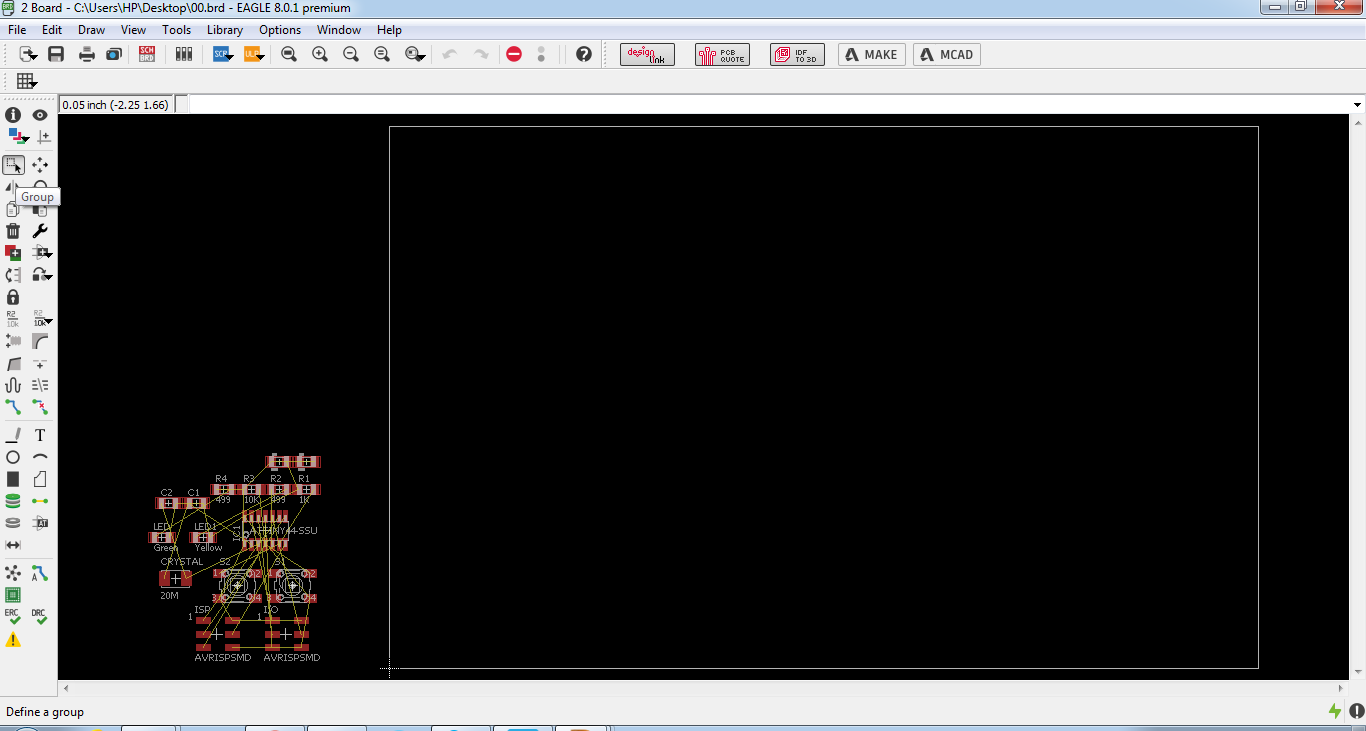
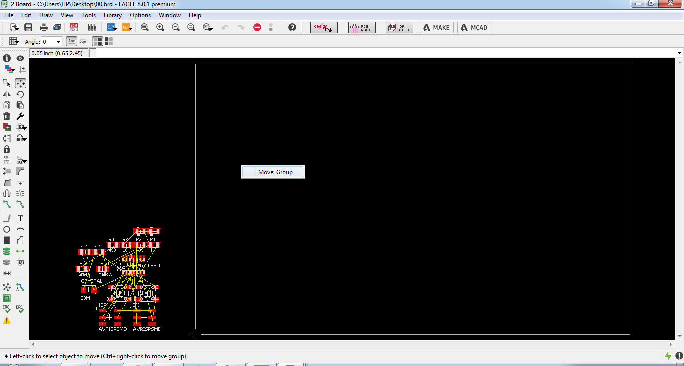
-I used group tool along with the move tool to place all the components in the working area. First I slelected the group tool and selected everything then selected the move tool, right clicked and chose move group.
-I used the move tool to place the components in a way that can help make the routing easier.

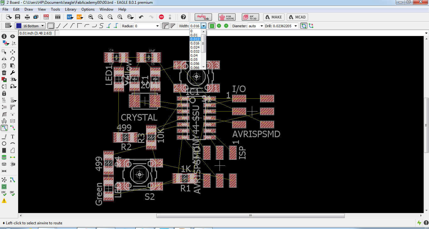
-After this I did the routing of the traces using Route tool. I selected 0.012 as the width for the traces.
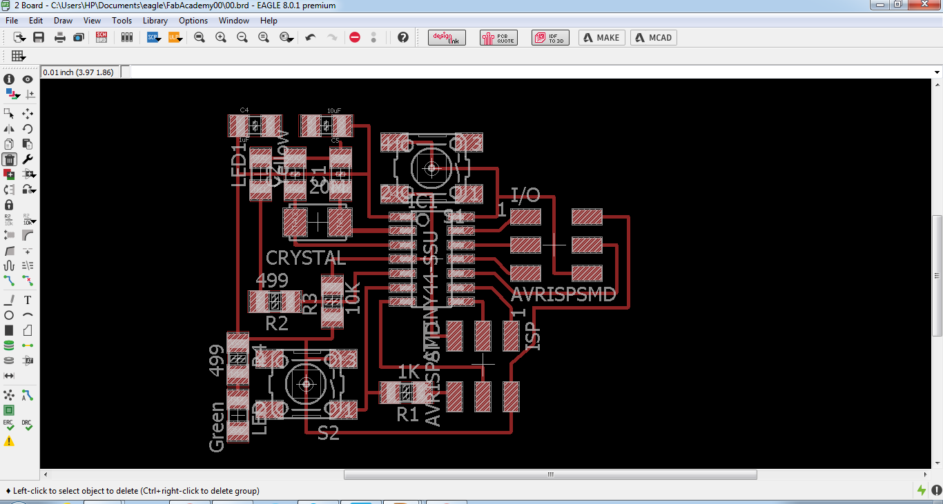
-I connected all the points together and this is how it looked after I was done.
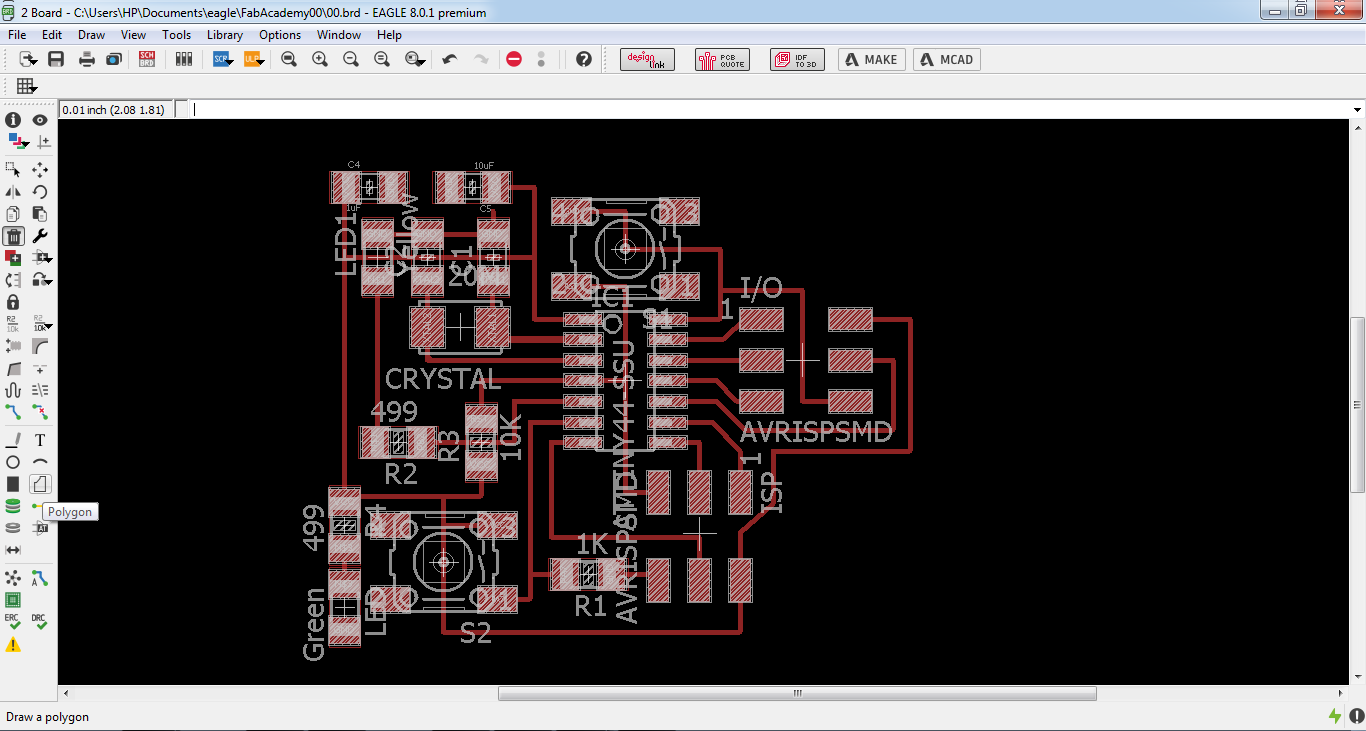
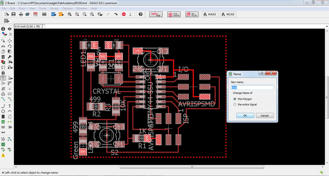
-I added a polygon around my traces as I wanted to have a ground plan. I started by selecting the Polygon tool
-To make this polygon as ground I right clicked one of its edges and chose Name and etered GND and pressed Ok.

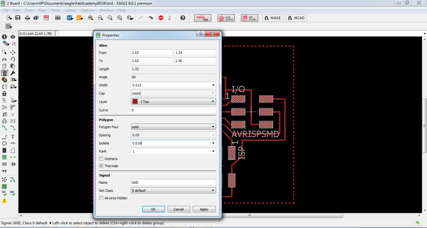
-I added isolation between traces and ground inorder to make the soldering easier. I right clicked one edge of the polygon, selected properties and changed the isolation to 0.019.

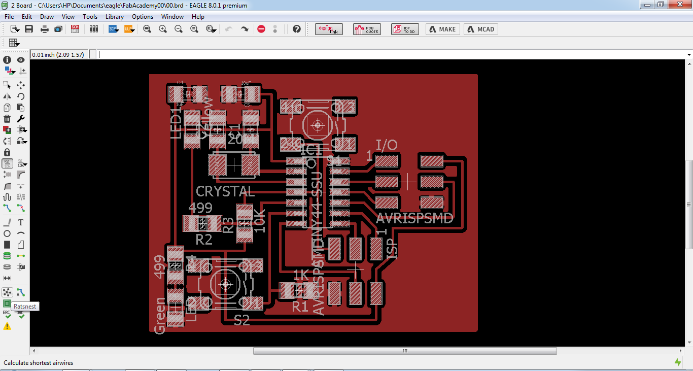
-Finally I pressed Ratnest to apply this ground filling to the polygon.
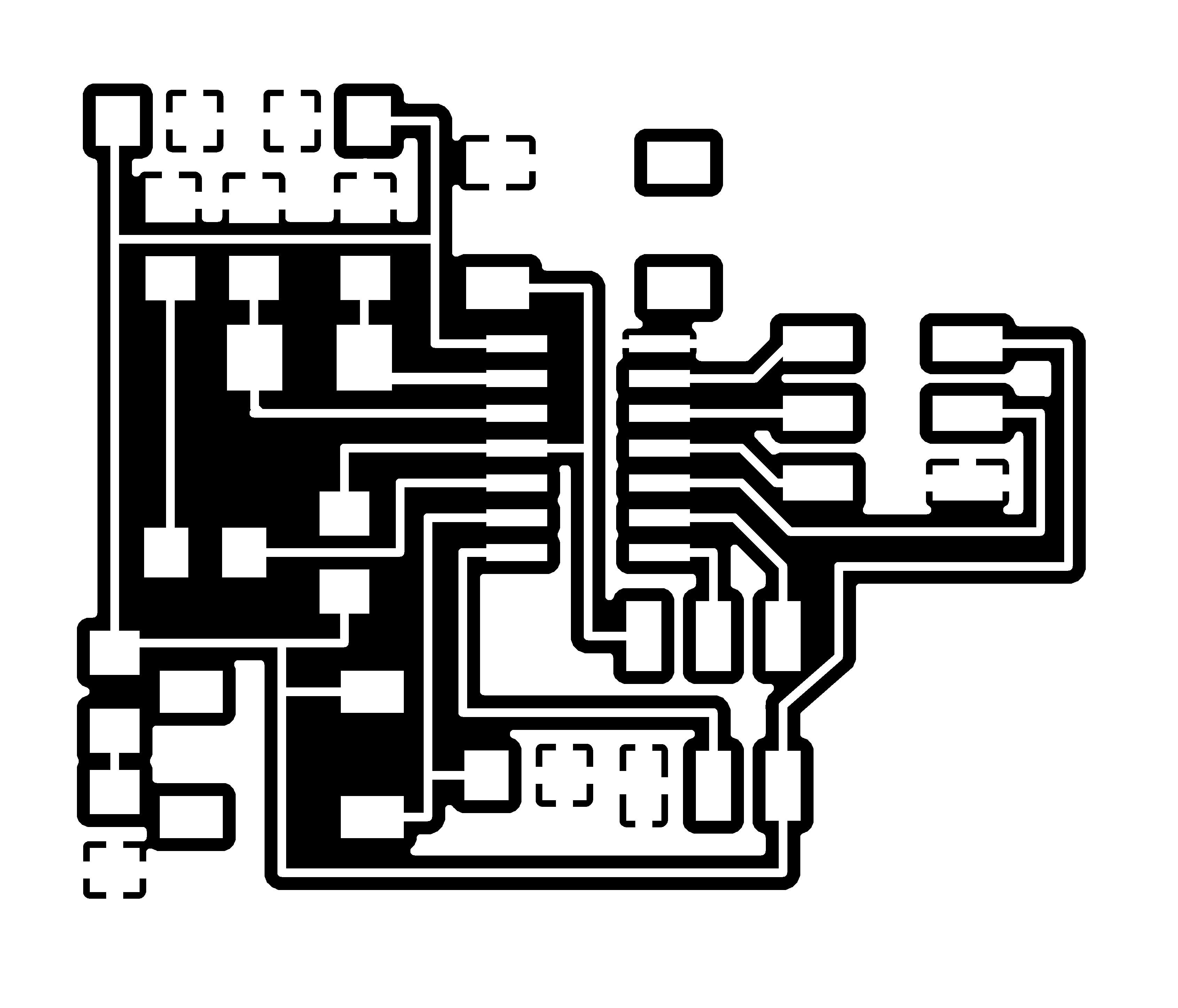
-I exported the board file as an image by going to File-->Export-->Image

-I selected Monochrom, 1500 dpi and Window.

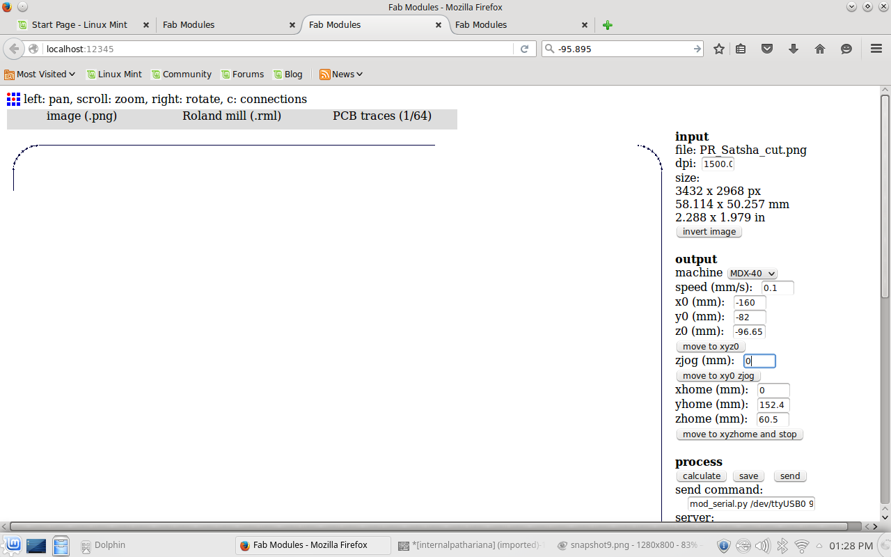
Milling
-First of all I connected to FabModules using the IP address of 127.0.0.1:12345 and then imported the image to it.
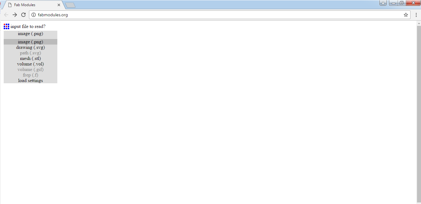
-I chose my Image and pressed Ok.
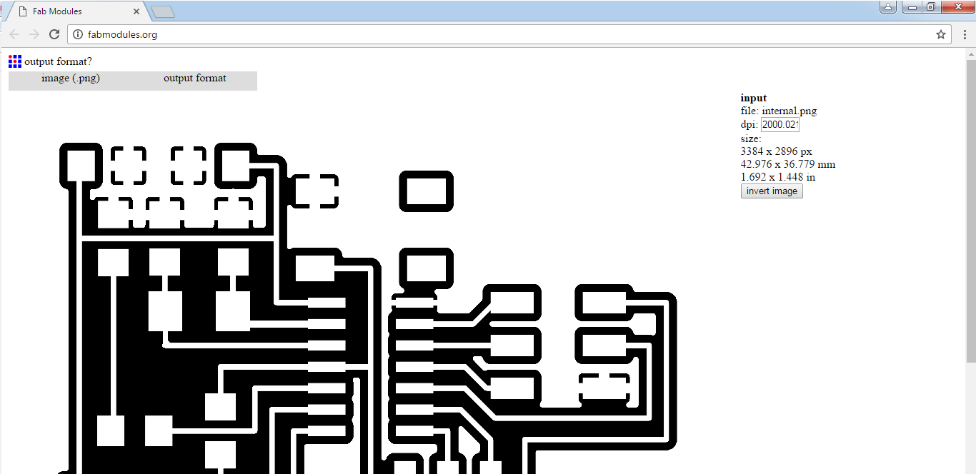
-Next thing to to is to choose the machine type by setting the output format, I chose Roland mill.
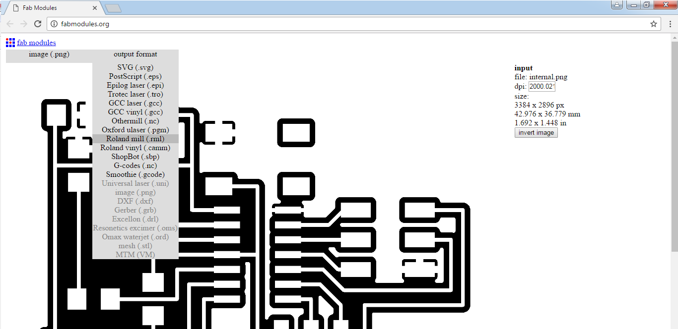
-I then choose the process type of 1/64 for PCB traces.
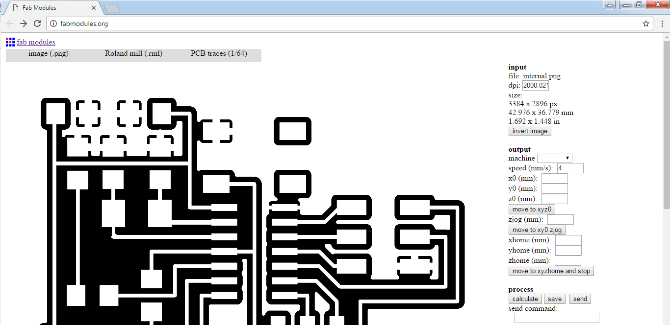
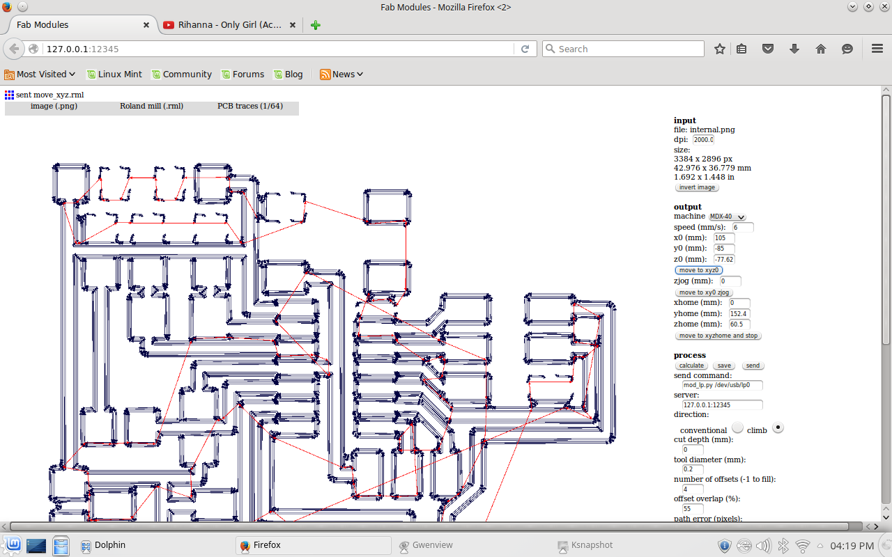
-Here are the settings I used for the internal paths:
-Machine: MDX40
-Speed: 6
-X0: 105
-Y0: -85
-Z0: -77.62
-ZJog: 0 (This has to be set to zero everytime the Z position is changed before moving the machine otherwise it is going to make the machine unresponsive)
-Send command: mod_lp.py /dev/usb/lp0
-Server: 127.0.0.1:12345
-Cut depth: 0.0
-Tool diameter: 0.2
-Number of offsets: 4
-Offset overlap: 60
Finally I pressed Calculate and that's what I got
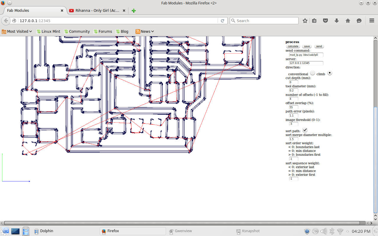
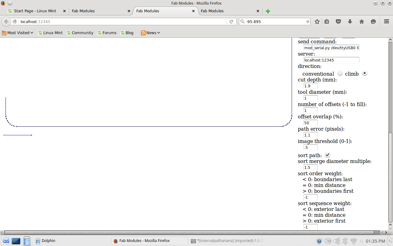
-I sent the job to the machine and after the traces were done and Next I had to launch the other job of cutting the board out.
-First I uploaded the image for the cut
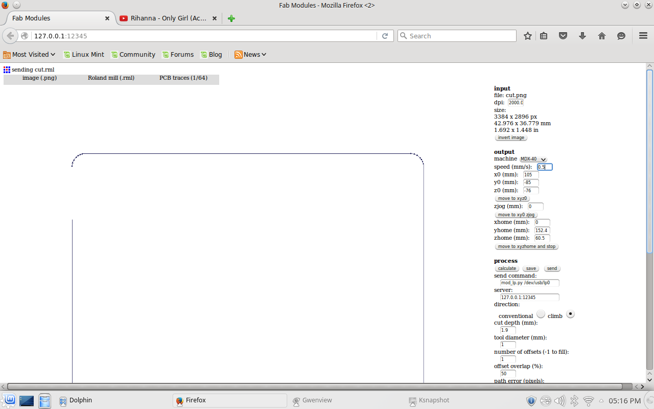
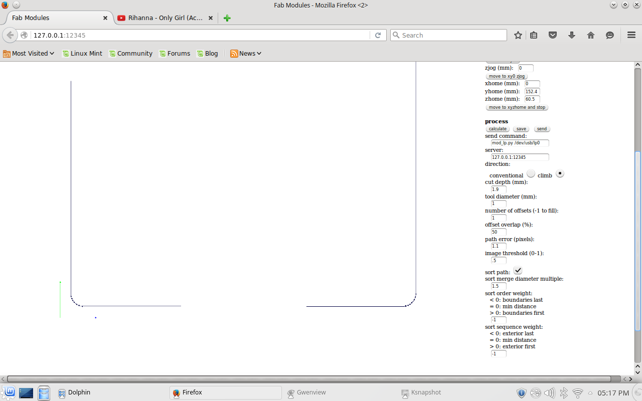
-Here are the settings for the cut:
-Machine: MDX40
-Speed: 0.5
-X0: 105
-Y0: -85
-Z0: -76
-ZJog: 0 (Again this has to be set to zero everytime the Z position is changed before moving the machine otherwise it is going to make the machine unresponsive)
-Send command: mod_lp.py /dev/usb/lp0
-Server: 127.0.0.1:12345
-Cut depth: 1.9
-Tool diameter: 1
-Number of offsets: 1
Finally I pressed Calculate and then sent the job to the machine
-The board is ready for the SMD components to be soldered on it.
Components:
ATtiny44 SOIC
20MHZ Crystal
2* MM Switch
2*10K 1206 Resistance
2*10Pf 1206 Capacitor
1μf 1206 Capacitor
10μf 1206 Capacitor
2*499 1206 Capacitor
2* 2*3SMD Headers
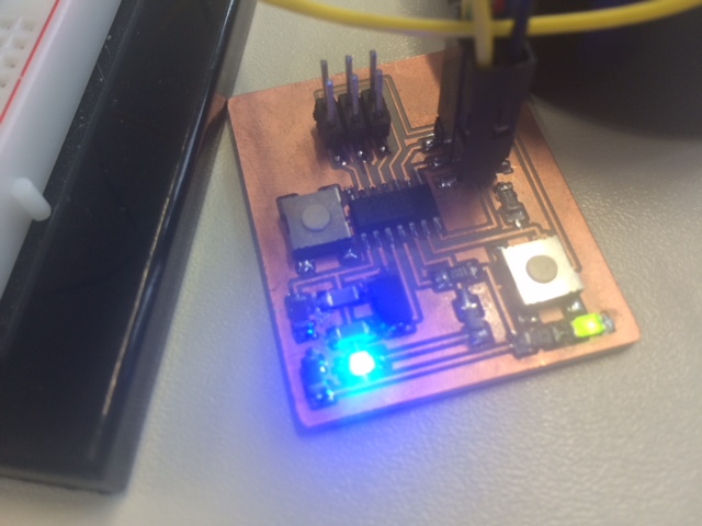
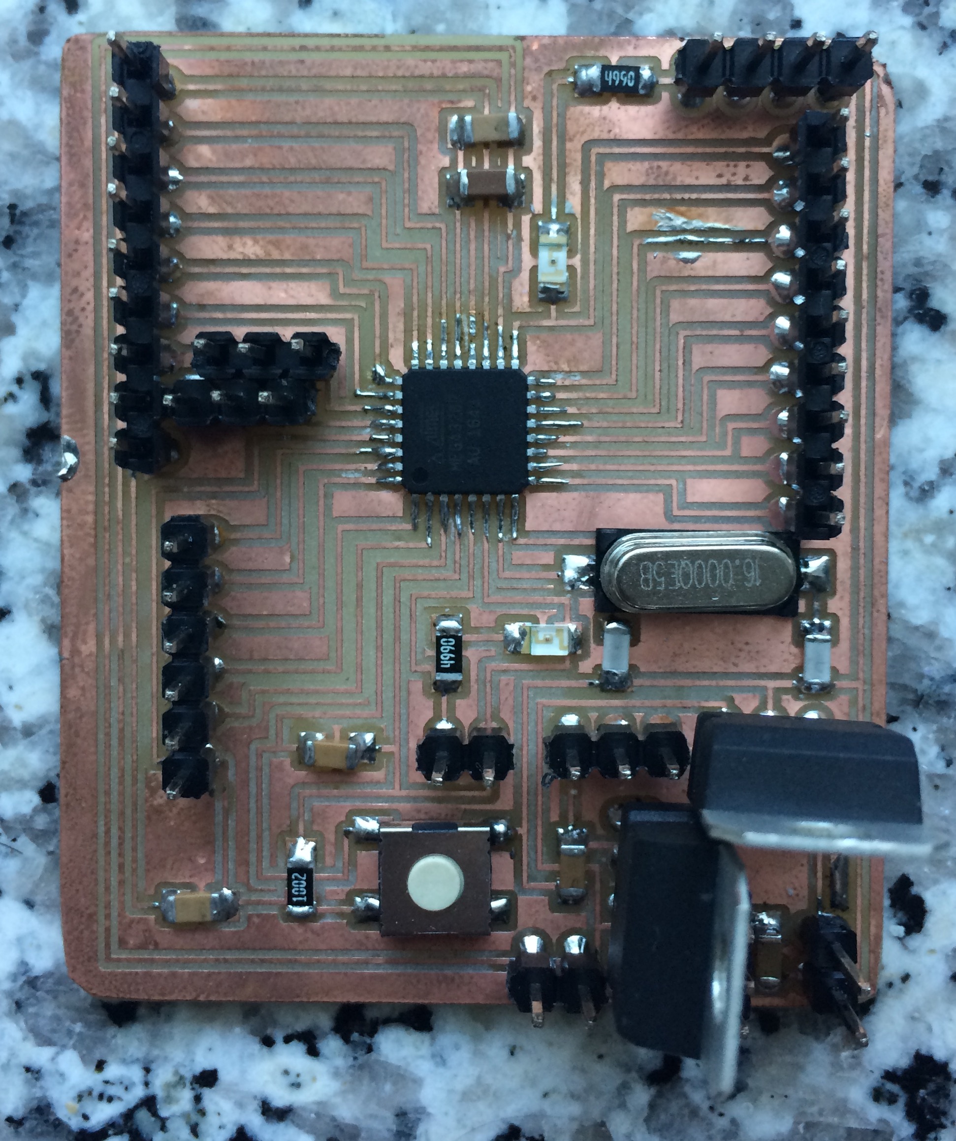
Final product:
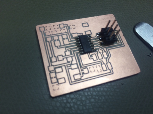
-This is how the board looked like after soldering the microcontroller
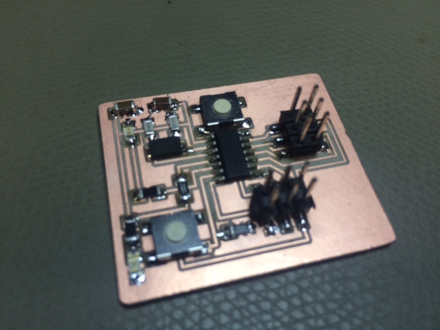
-This is how it looked after soldering the rest of the components
Testing
I used Arduino IDE along with an arduino Uno board to burn the bootloader to my board and try to upload simple blink sketch to make sure it's working
-I connected the Arduino, chose the right port from tools and Uploaded the ArduinoISP sketch to it

-I diconnected the Arduino, and connected my board to it as follows:
ATtiny44 Pin 1 to Vcc.
ATtiny44 Pin 14 to ground.
ATtiny44 Pin 4 (Reset) to Arduino Pin 10.
ATtiny44 Pin 7 (MOSI) to Arduino Pin 11.
ATtiny44 Pin 8 (MISO)to Arduino Pin 12.
ATTiny44 Pin 9 (SCK) to Arduino Pin 13.
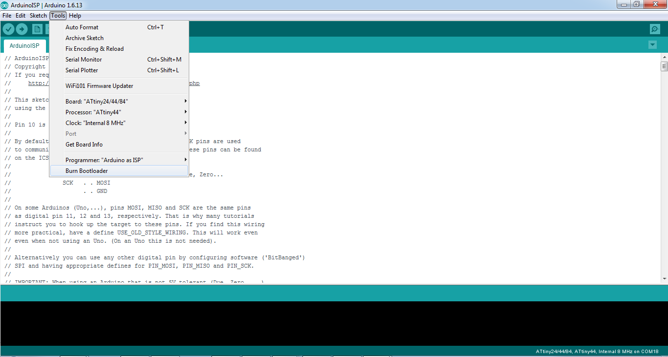
-I chose the right settings for burning the bootloader:
Board ATtiny25/45/85
Processor ATtiny45
internal clock to 8MHz
Programmer ArduinoISP.
Finally I pressed Burn bootloader.
-After this was done I went to File-->Examples--> 01.Basics and chose Blink. I modified the LED pin to 8 as that was the one I connected the LED to. Finally I uploaded the sketch using programmer.

Another PCB Design Task
As part of the Fundamentals of Digital fabrication course that took place in the FabLab of Kamp-Lintfort I had an assignment which was to make some modifications on a PCB called satshakit made by The greatest Daniele Ingrassia . The design is for a micro controlled board using Atmel ATmega328p chip and it is capable of doing what an Arduino Uno can do.
I used Eagle also to design the board.
Modifying the design
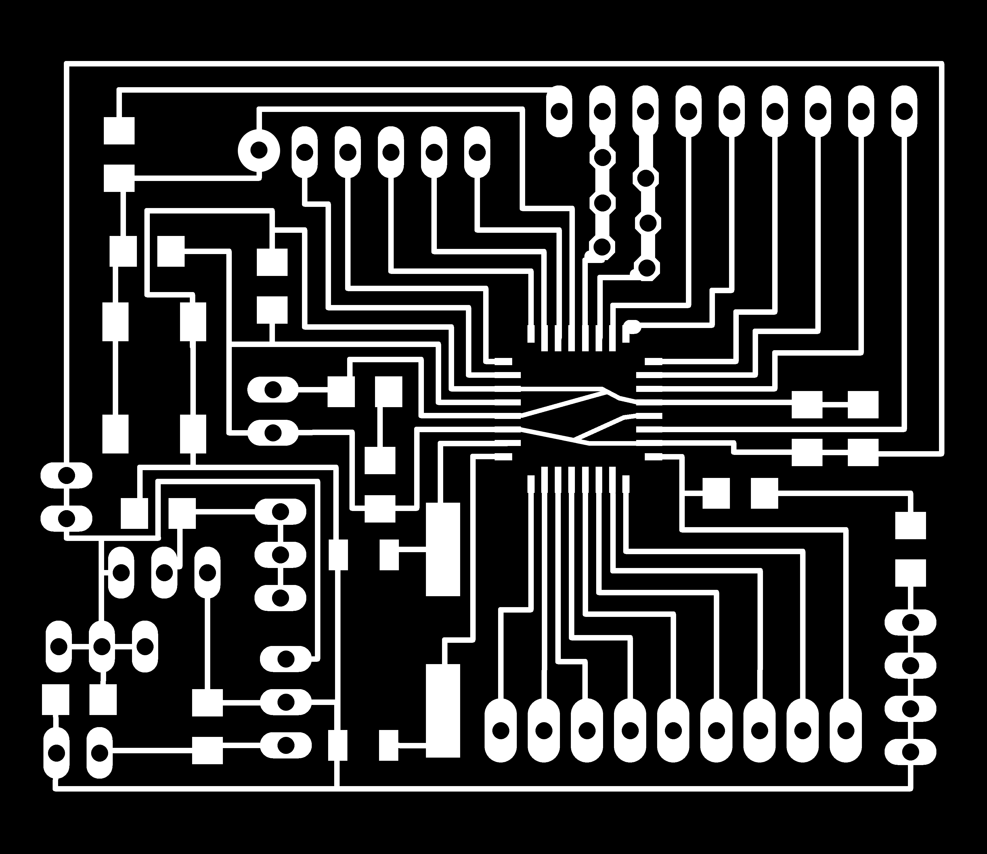
This is how the original design looks like.
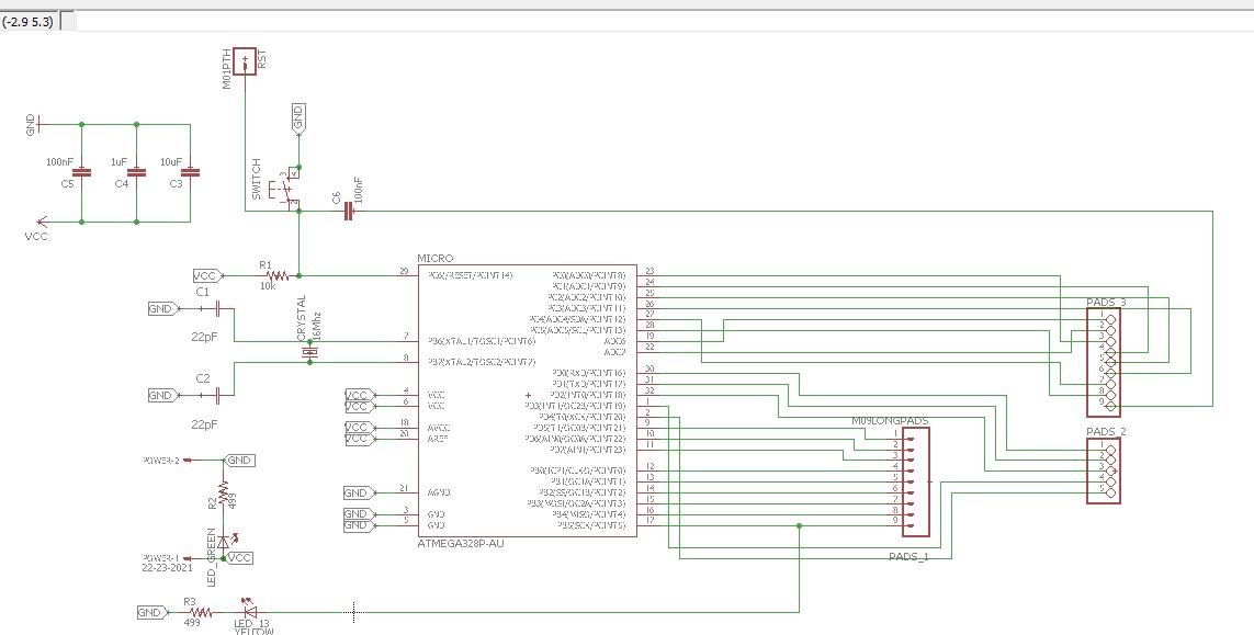
First step was to download the original schematic file and open it to add my modifications. I decided to make four as follows:
-First to add extra pins for I2c to be able to connect more than one sensor to the board .
-Second to add extra pins for Ground, VCC 5volts and 3.3 Volts .
-Third to add a 3.3v regulator circuit to be able to take 3.3v from the board.
-Fourth to add a 5v regulator to be able to connect the board directly to a 9v battery.
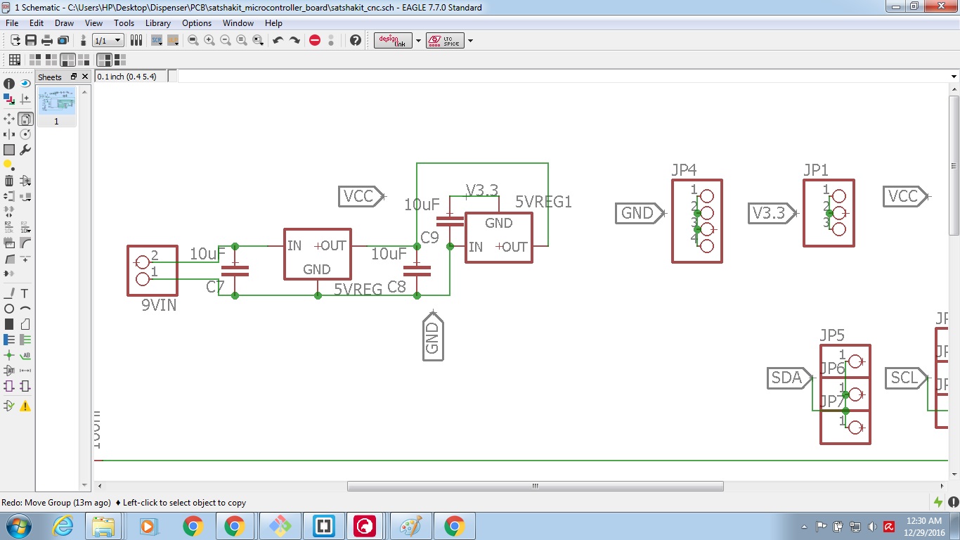
First Modification:
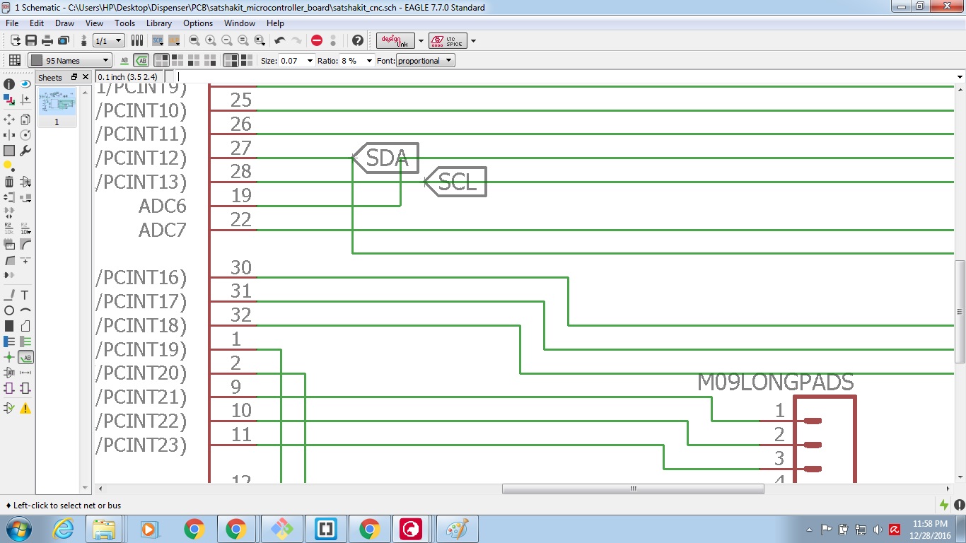
Right click the wire connected to pin 27 of the IC and click on name.
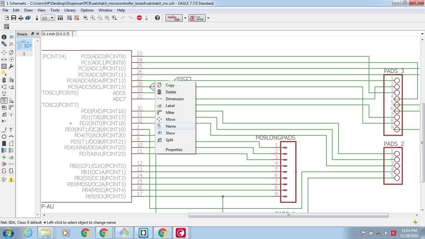
Type SDA and click OK.

To add a label to the wire with its name Click on Label-->check bottom left corner of the image.

I like to use the Xref -->check upper left corner of the image.

Click on the same wire you named SDA, This is how it should look.
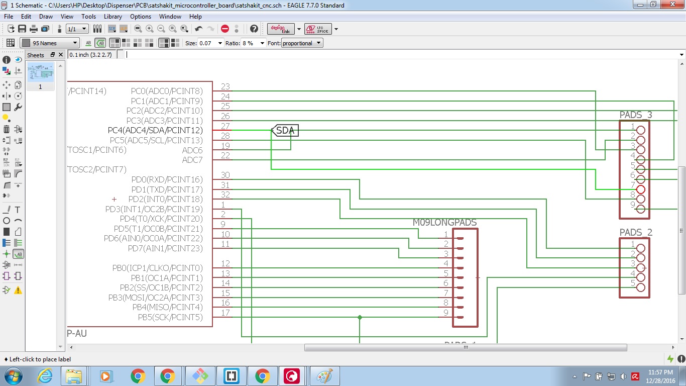
Do the same for the other pin of the IC naming it SCL.
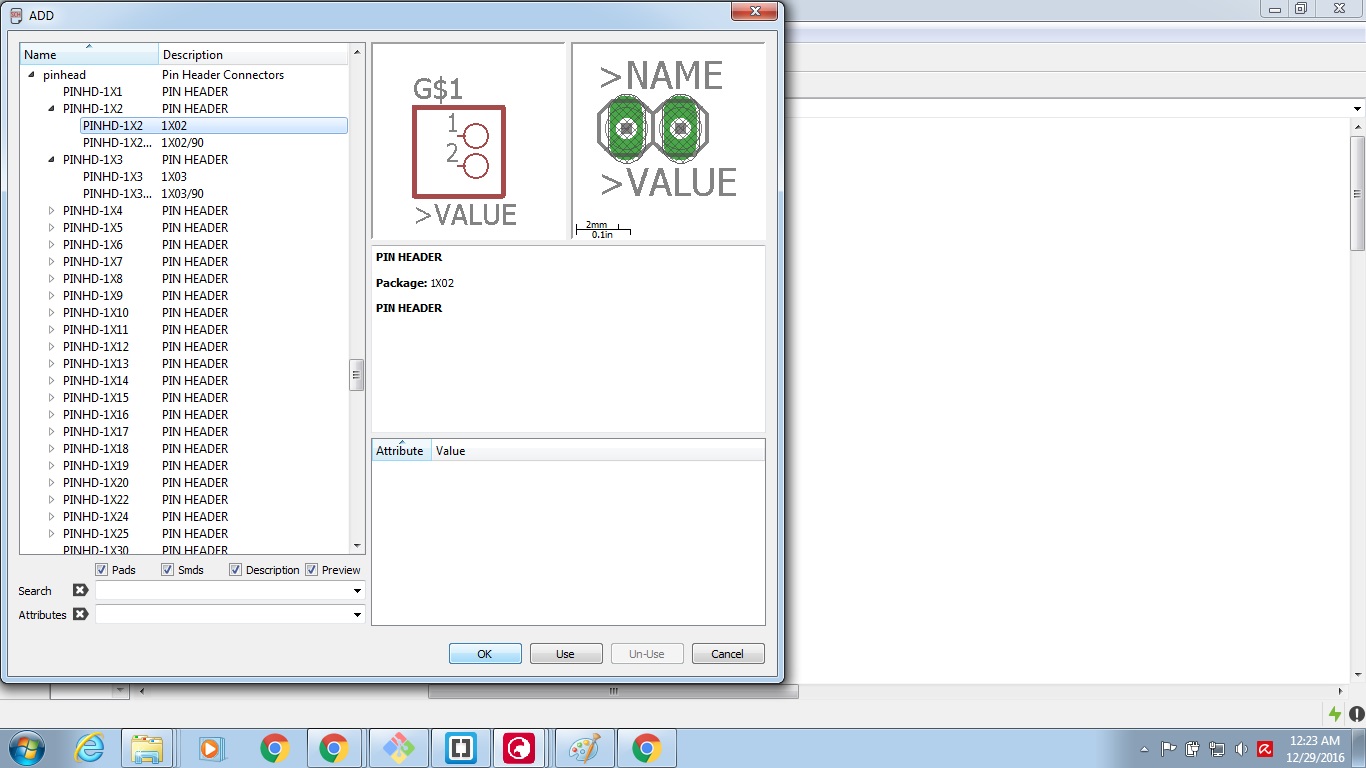
Now add the extra pins, Click on add button -->check upper left corner of the image.

Scroll down to Pinhead. And since I chose to add 3 extra I chose the third one and then the first one. Then press OK.

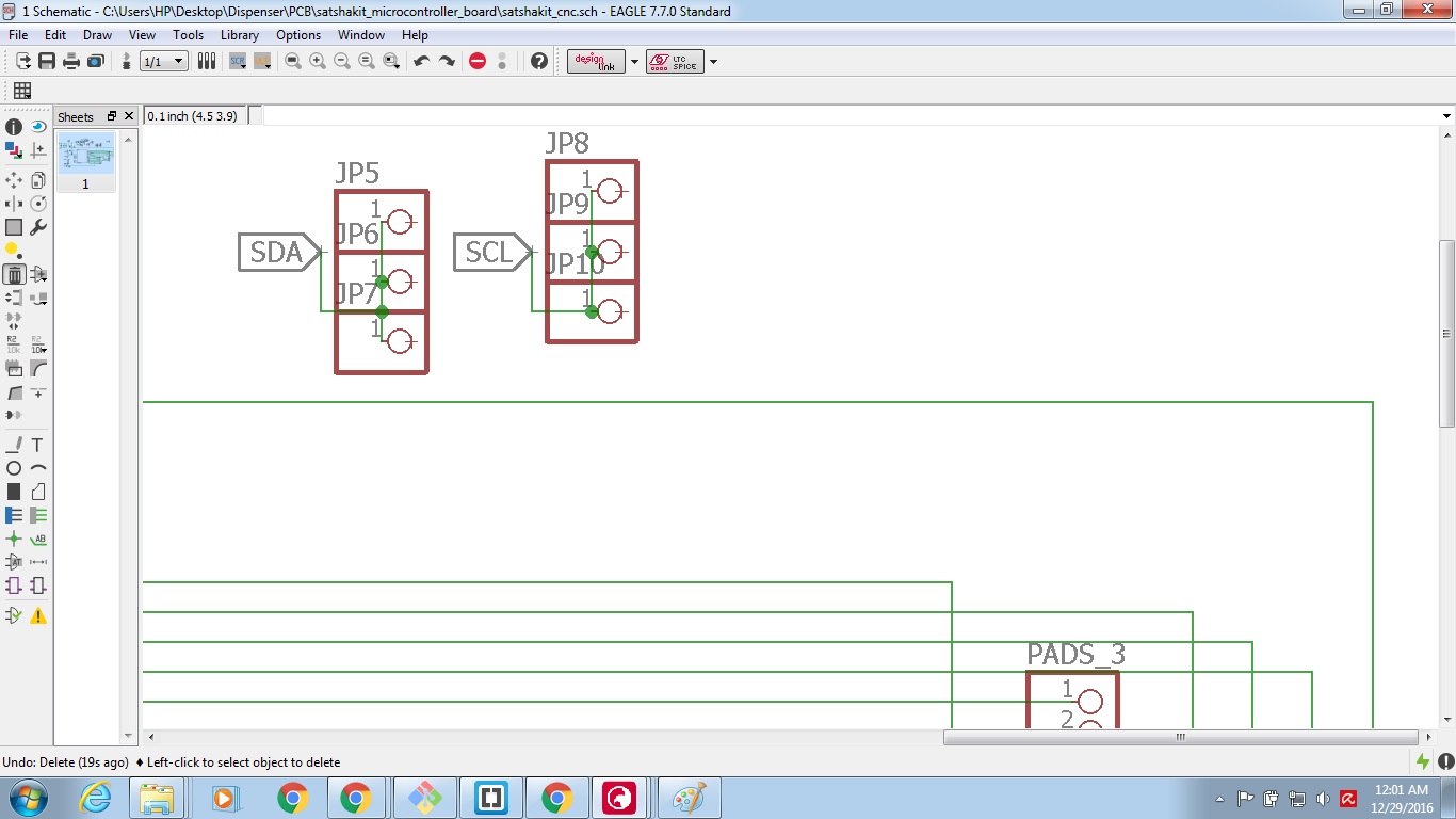
Click in the place you want add the part, Add 2 of these. And then click on Net -->check lower left corner of the image.
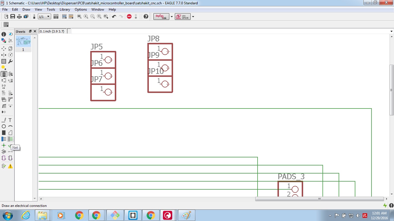
Connect the pins as shown and then name the wires and add labels same as before.
Second Modification:
Add some pin header groups for VCC, Ground and 3.3V using the ADD button. Connect them using Net button, name them and add the labels as shown.

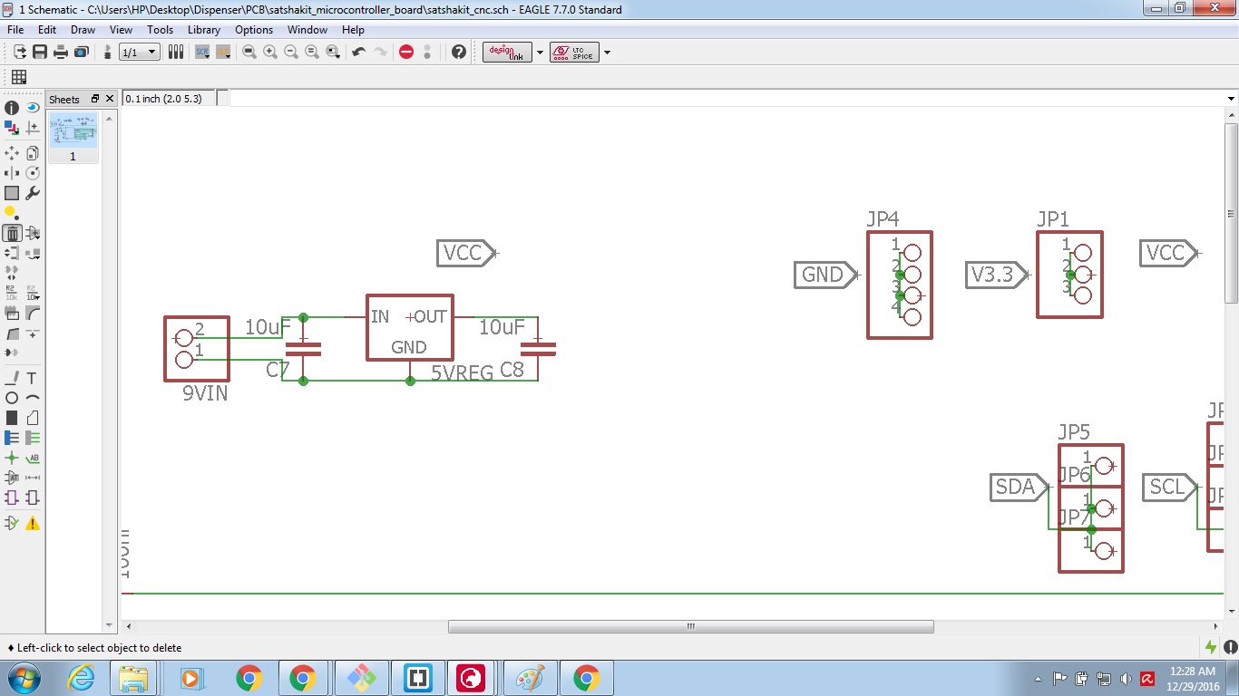
Third Modification:
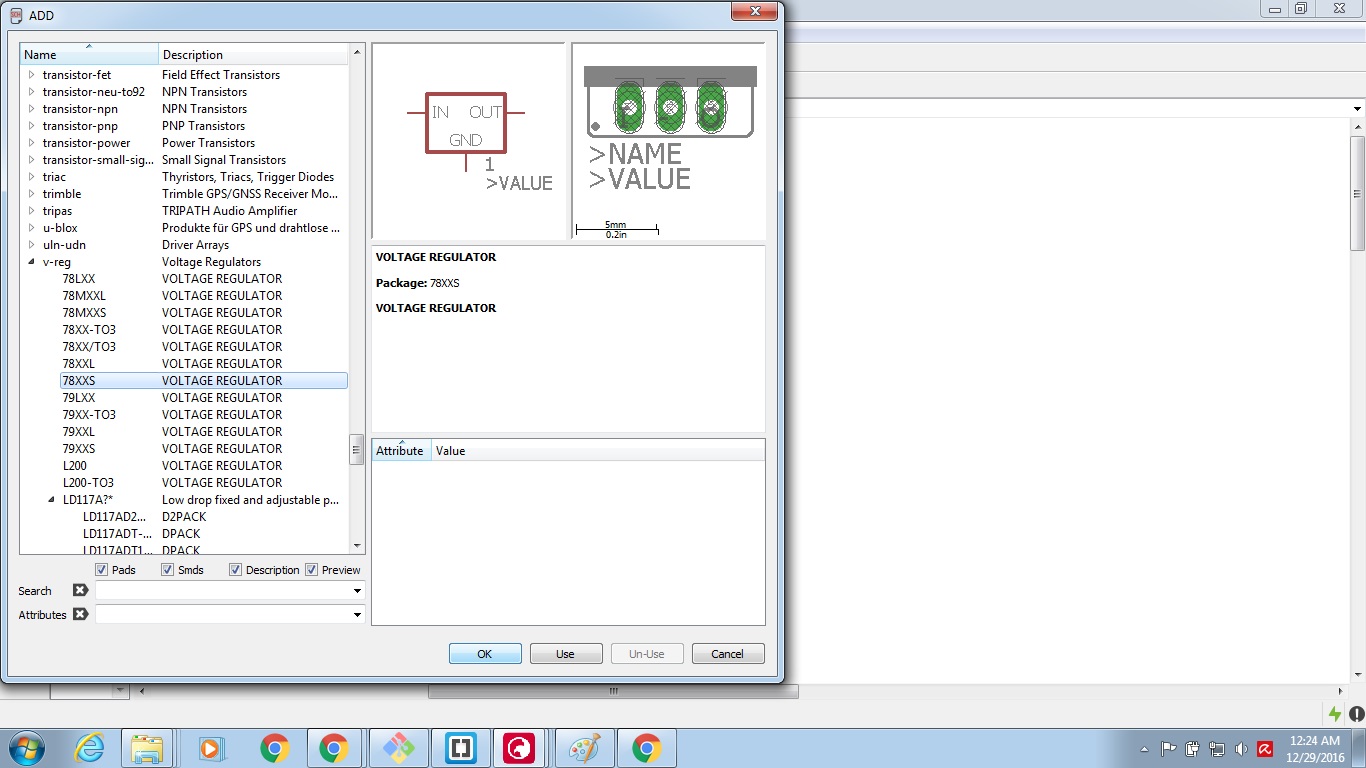
We need to add pin headres to connect the battery, voltage regulator and capacitors.
First place the pinheaders .
Scroll to find vreg and choose the one shown in the picture.
As we need to add 10uF capacitors the easiest way would be to copy the one we need from the design.
Click on the copy icon and use it to copy the part you want -->check upper left corner of the image.

Add them as shown.

Connect them using Net button as shown.
Fourth Modification:
Add another Vreg and a capacitor as before.
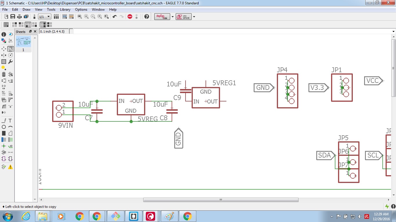
Connect them as shown. The reason the connection is like this is because I used the same Vreg as in modification three although the Pinout of the 3.3Vreg is not the same as the 5V but I couldn't find it in eagle.
Time to edit the Board file .
Click on switch to board button .

My Idea was to free some space in the lower left corner of the board.
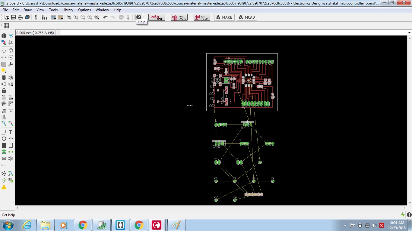
Click on Ripup and remove all wires connecting the crystal and then right click on it and move it to the right.

Now connect the wires back using the Route button next to Ripup.
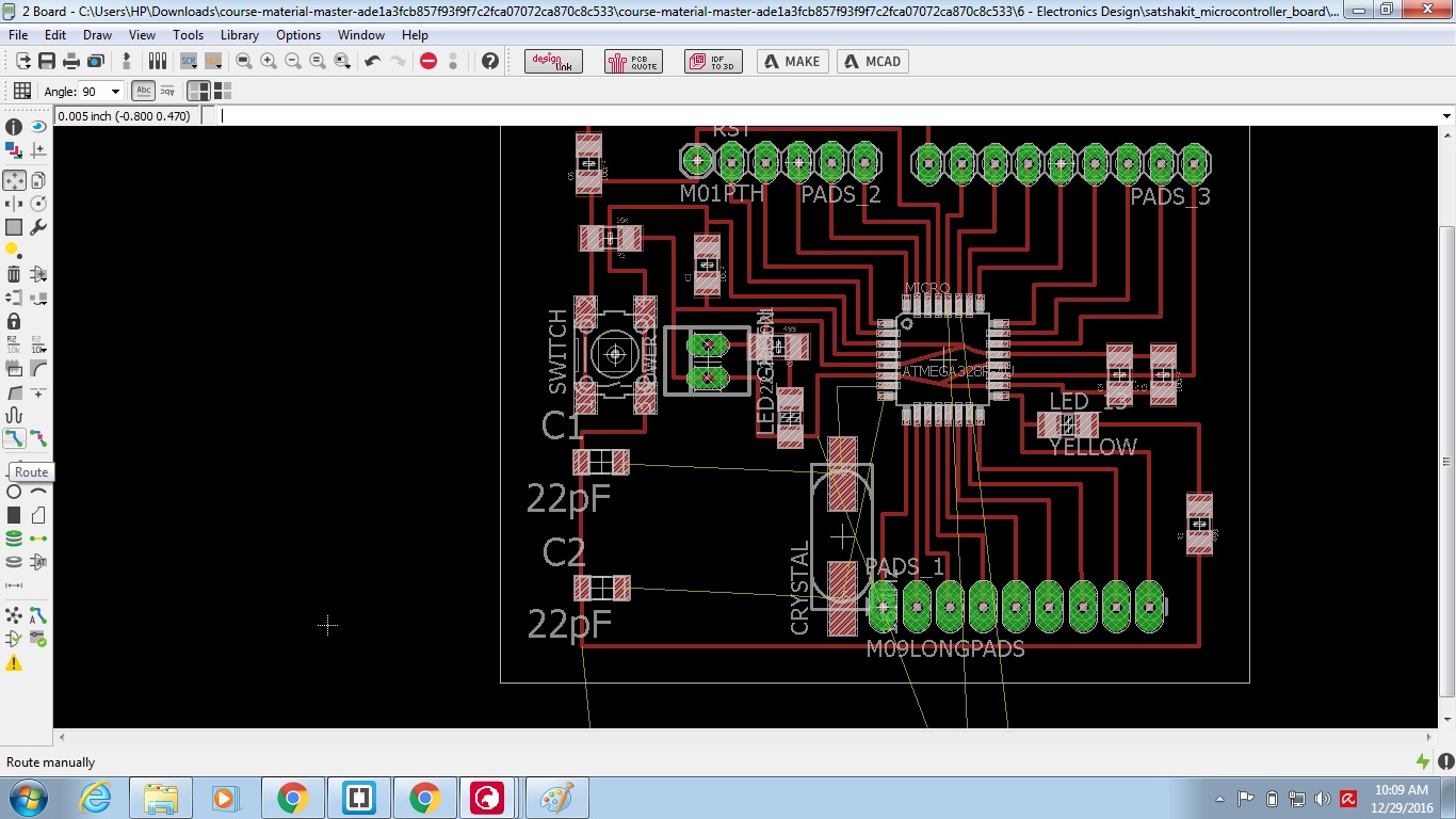
Use the width of 0.012 and make sure you are on the top layer all the wires should be red.

Now We have the place we wanted.

Using the same commands Move, Route and Ripup try to arrange all the components in the area. This is how my version looks like.
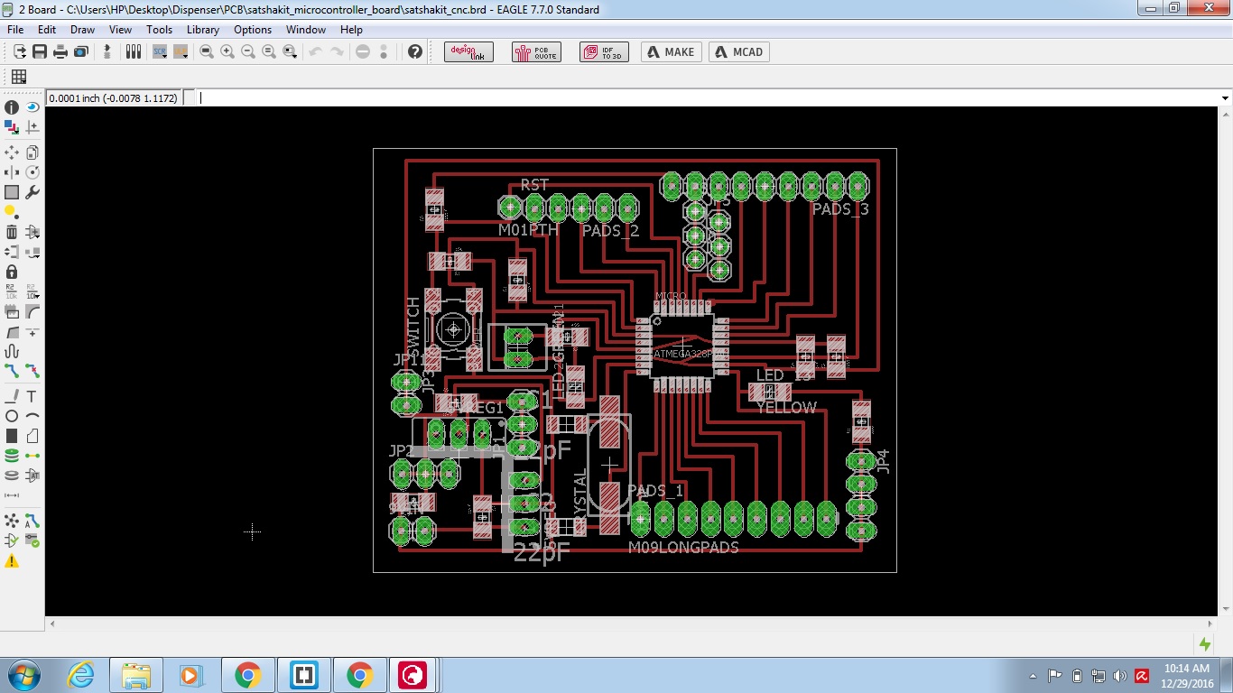
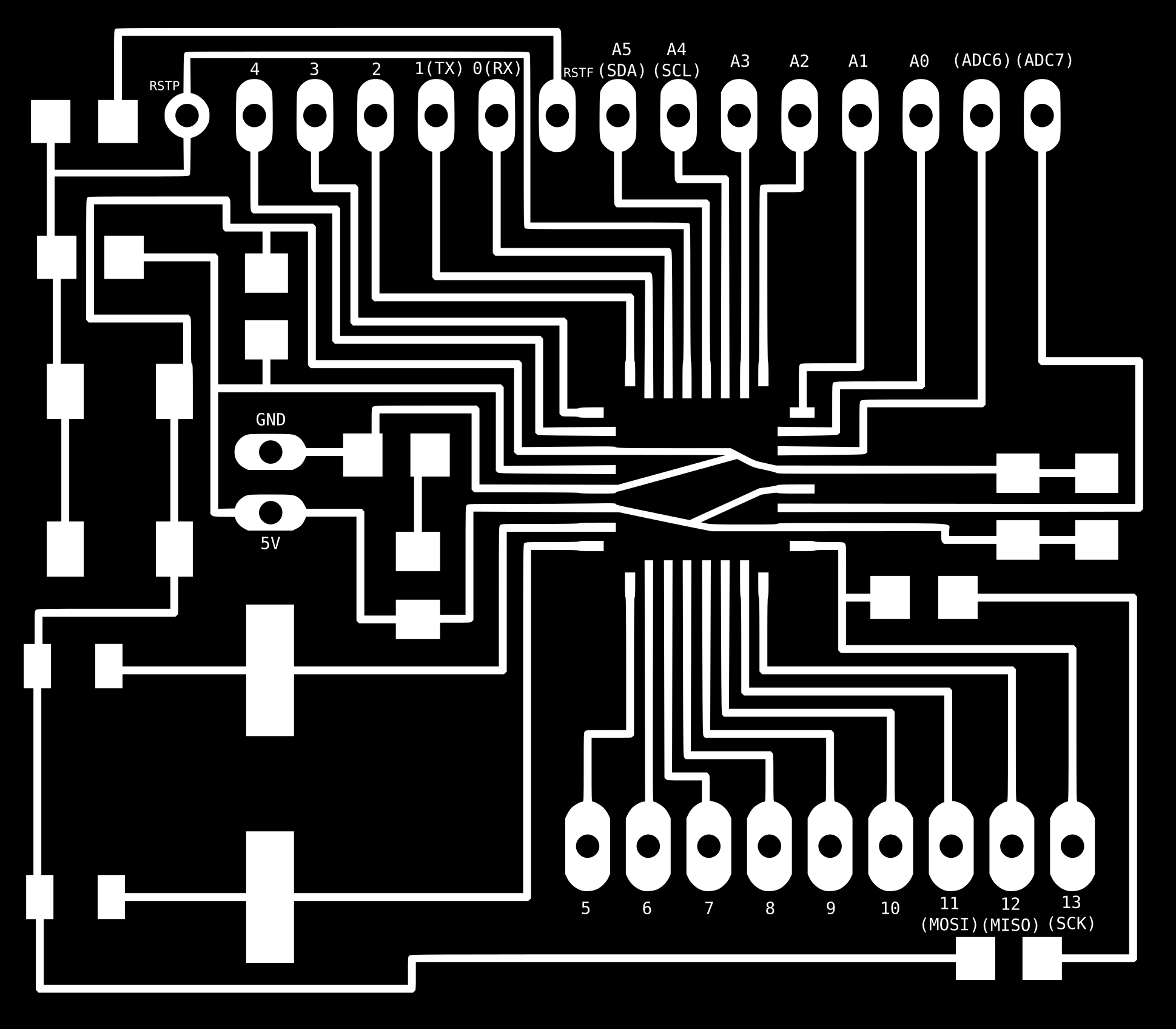
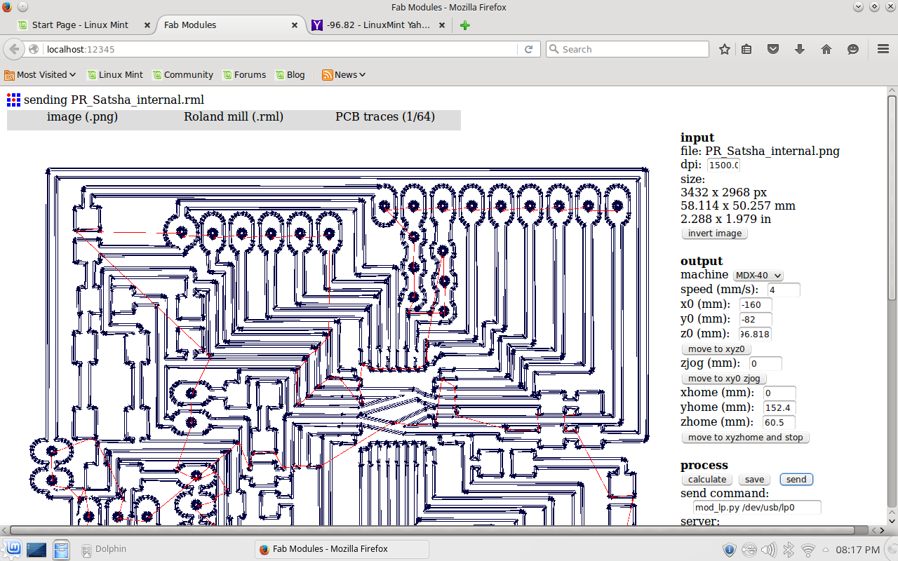
Finally I exported the design as shown above.

Here are the 2 images to be used for the CNC machine. You can see that i have edited the image of internal path to enhance the final product. This is just an extra step for better quality you can do this using any photo editor.

Milling the PCB
For this assignment I used Roland MDX40A CNC machine and Fab Modules To control it.
This time I used the server computer connected to the CNC machine directly.
The import step is already shown in the previous documentation.
Here are the settings:
Machine: MDX-40
Speed: 4
Send Command: mod_lp.py/dev/usb/lp0
Server: Localhost:12345
Cut depth: 0
Tool diameter: 0.2mm
Number of offsets: 5
Offsets Overlap: 55

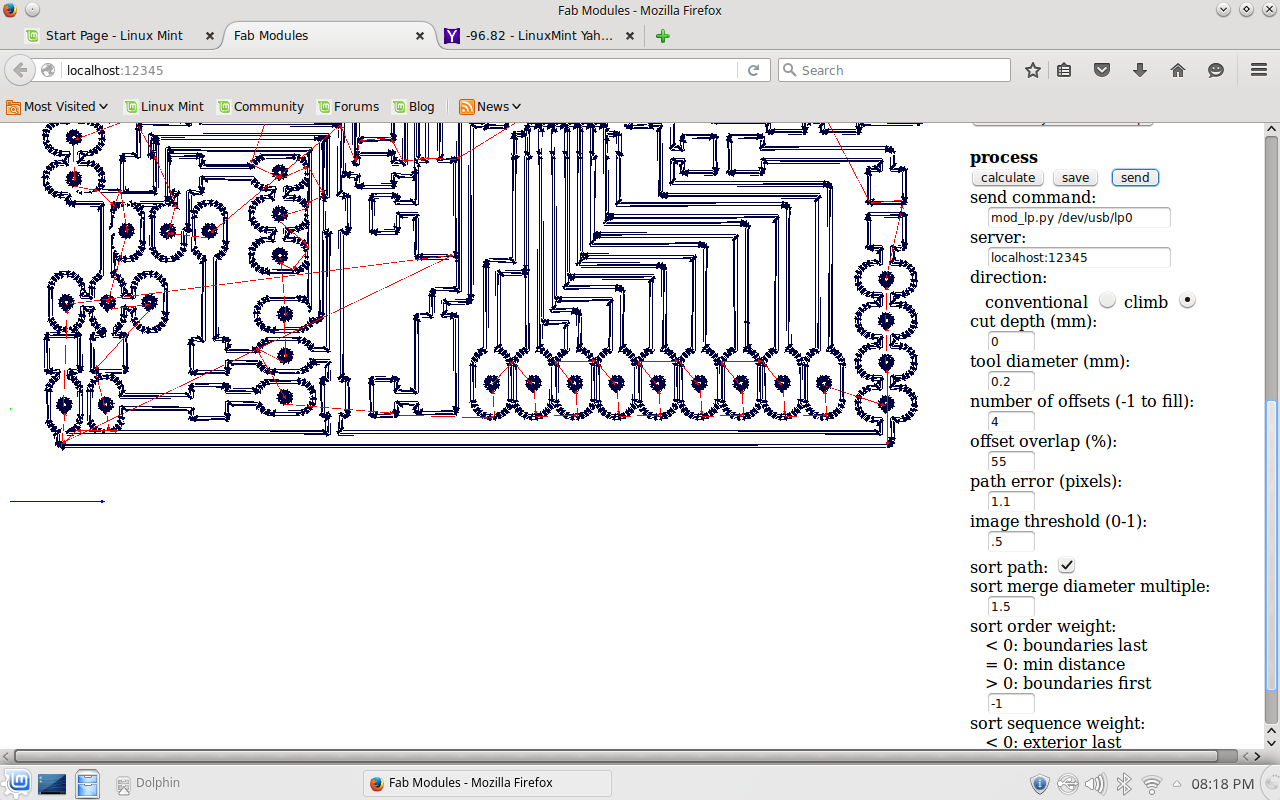
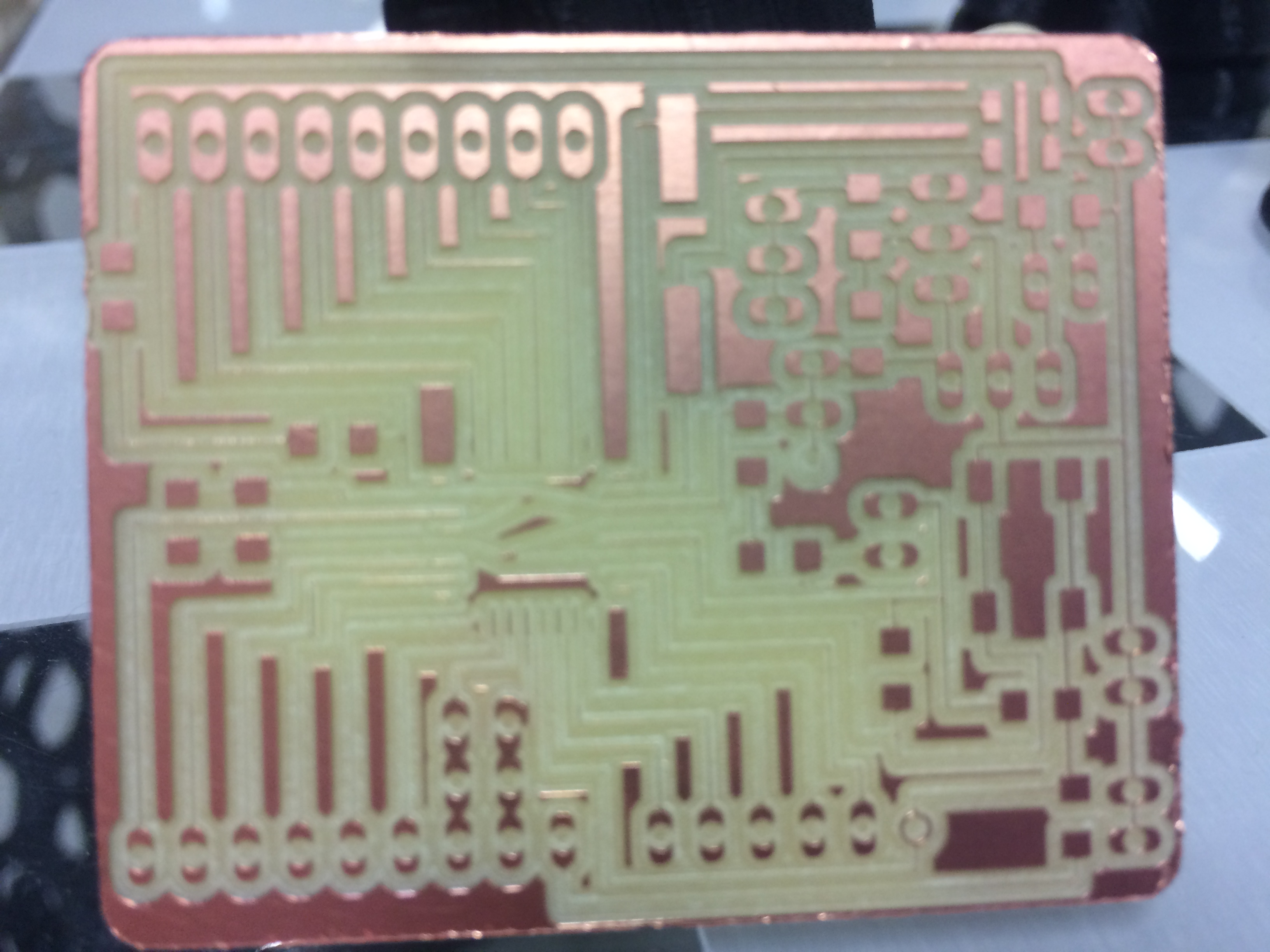
This Trial was a faluire because I went too deep into the material so I lost some of the copper traces.
I changed the settings as follows and went for a second try.

Time to cut the successful board out.
Final product