<-- Week 5
WEEK 6
[ELECTRONICS DESIGN]
Week 7 -->
WEEK'S GOALS:
IDEAS THIS WEEK:
ACHIEVEMENTS THIS WEEK:
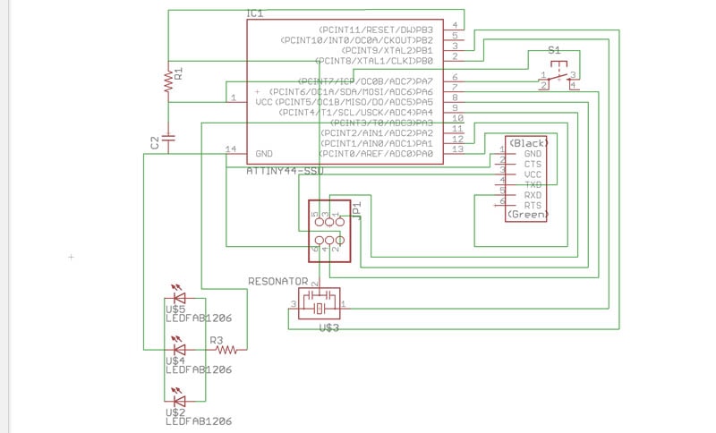
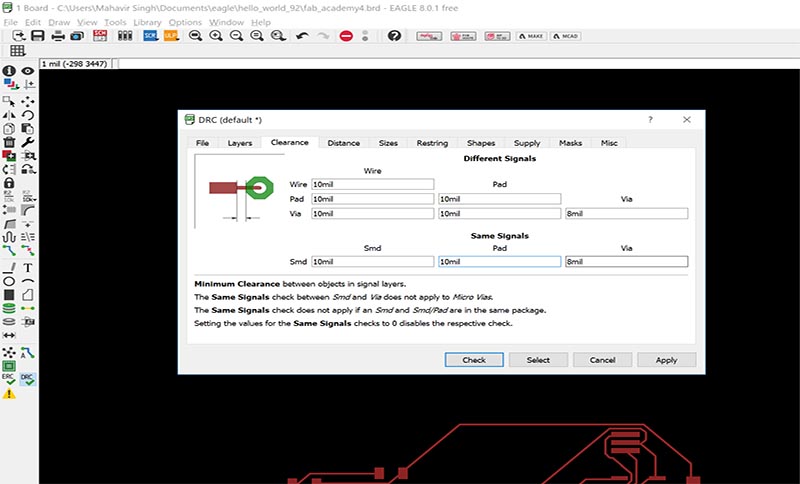
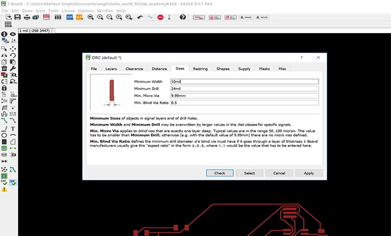
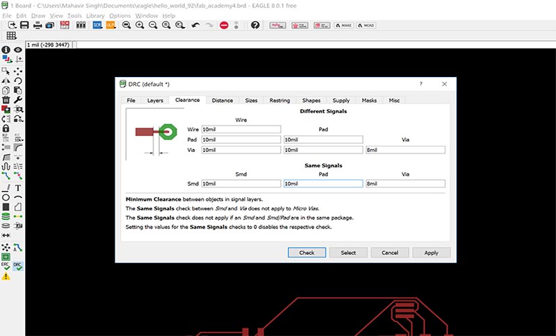
Electronics:1. Circuit Design
- Got refreshed with data on diodes, Leds, Capacitors, Resistors, ICs, Zeners etc. by our instructor
- Got familiarised with Autodesk Eagle by our instructor
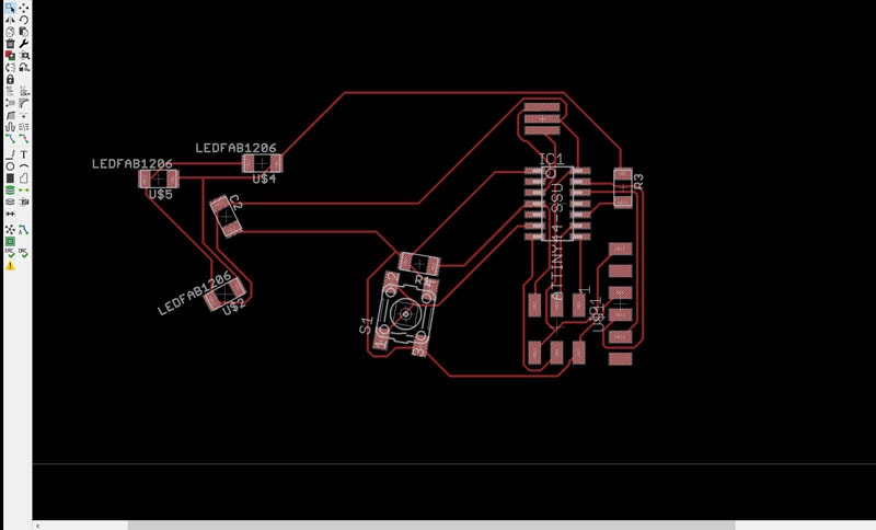
4. Board Routing
5. Populating of board
6. Try for Programming
TASKS AT HAND:
<-- Weeks Overview
Day 36
[ Preparing Files ]
Day 37 -->
1. Troubleshooting Laptops of my peers installing Ubuntu
2. Editing my Website
After a very informative Recitation with Dr. Neil, I sat for an hour or two to think of ideas regarding my assignment and how i plan to go about it. Went through softwares suggested by other fabbers like 123D Circuits and EAGLE and also different types of customised circuits online.
<-- Day 36
Day 37
[ Parallel Designing ]
Day 38 -->
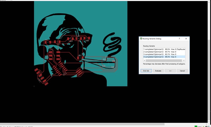
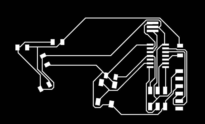
1. Autorouted with different orientations keeping the customised board shape in mind.

<-- Day 37
Day 38
[ Photoshop Routing ]
Day 39 -->
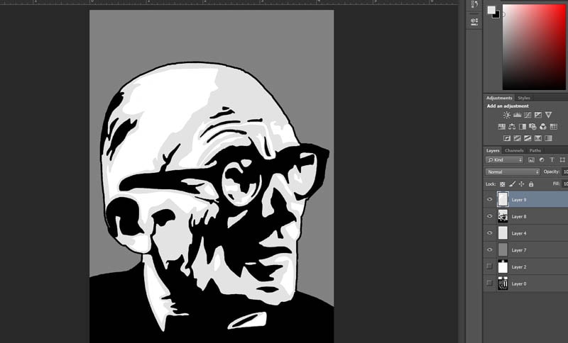
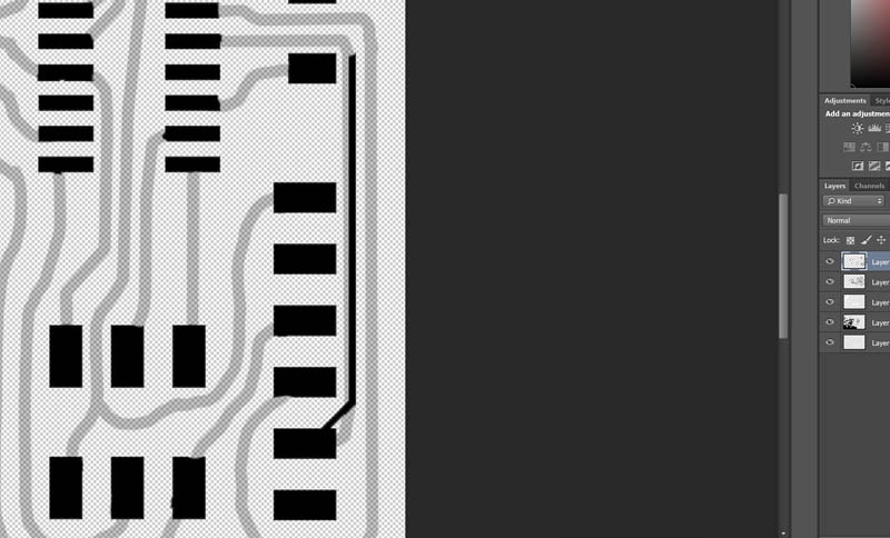
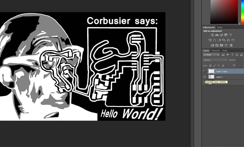
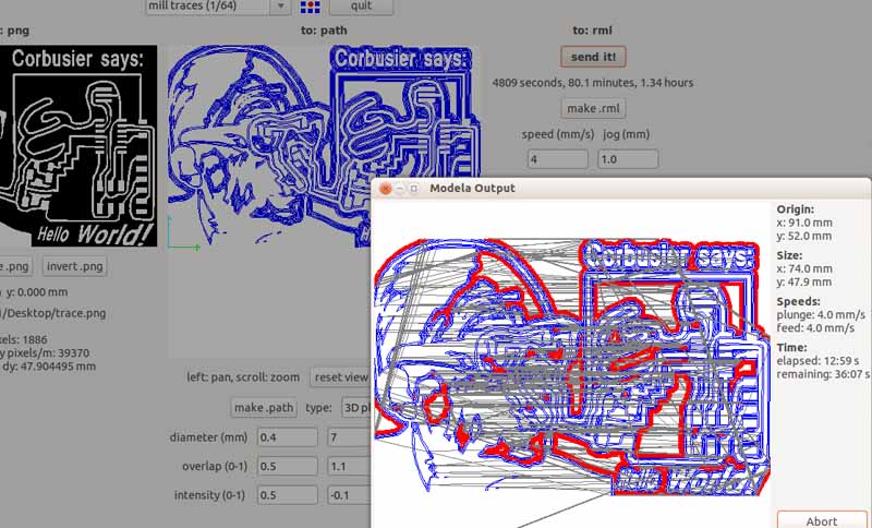
1. Imported Indexed PNG to Photoshop for Routing
2. Developed 3 layer routing image-Trace | Shine | Cut (Cut wasnt needed-file size just fit in the FR board)
3. Manual routing according to shape.

<-- Day 38
Day 39
[ Routing Time ]
Day 40 -->
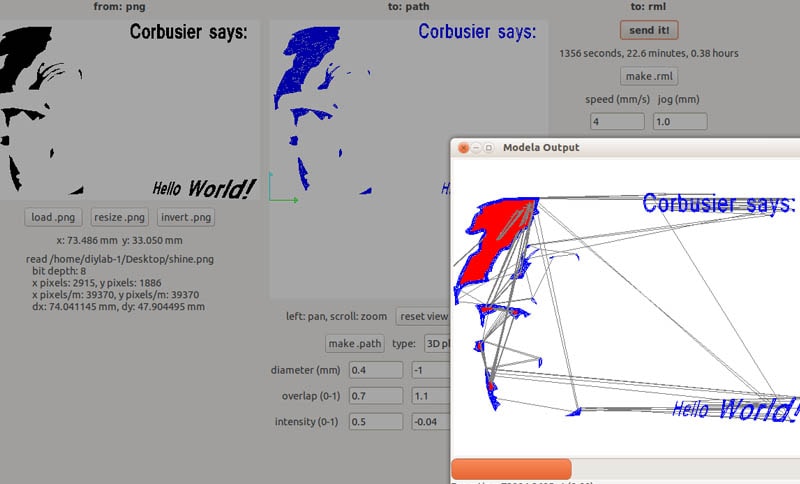
- 1.Tested my Shine Layer with 0.02 mm cut depth.
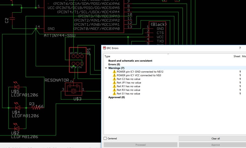
2. Went through the test board scanning for possible shorts and correctinng my trace file accordingly
3. Check list for routing-> bed leveling + more
So the order to achieve this shine layer and integrate it within your board is as follows:
1. We route the shine layer first (just in case so we know we will get it on our board without mistakes and copper coming out) @ 0.02mm cut depth
2. We then route the trace file @0.06 mm cut depth
3. Then the cut file @1.7 mm cut depth.

<-- Day 39
Day 40
[Populating time]
Day 41 -->
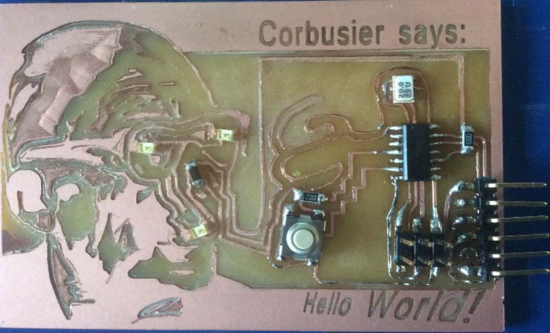
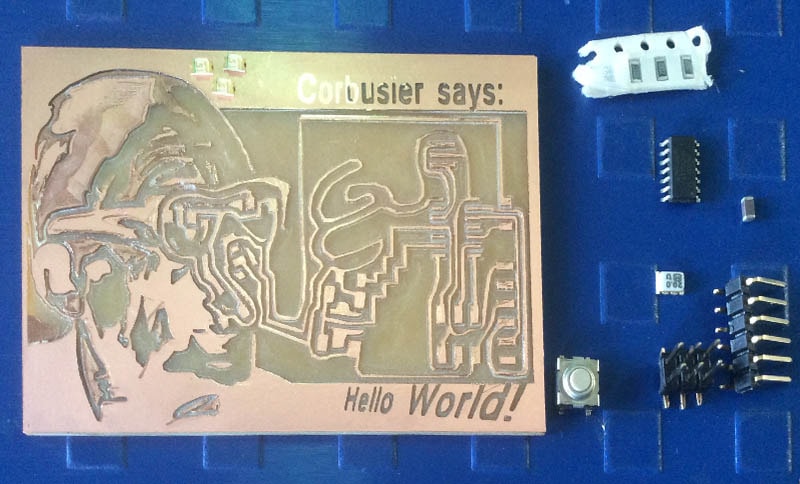
- 1.Gathered all components
2. learnt how to stuff it and solder
3. Learnt importance of Flux and how to add and remove solder
4. Loved arranging the components while soldering
I liked this week as it forced me to not sit on laptop whole day designing and working but also do hands on work . I discussed with Yogesh ji my final project and how i plan to improvise it with time and use Shopbot before the given week so that i am able to figure out ideas to improve my final project.
<-- Day 40
Day 41
[ Ready for Programming]
Day 42 -->
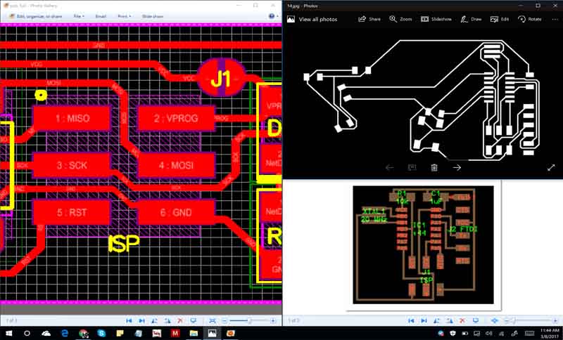
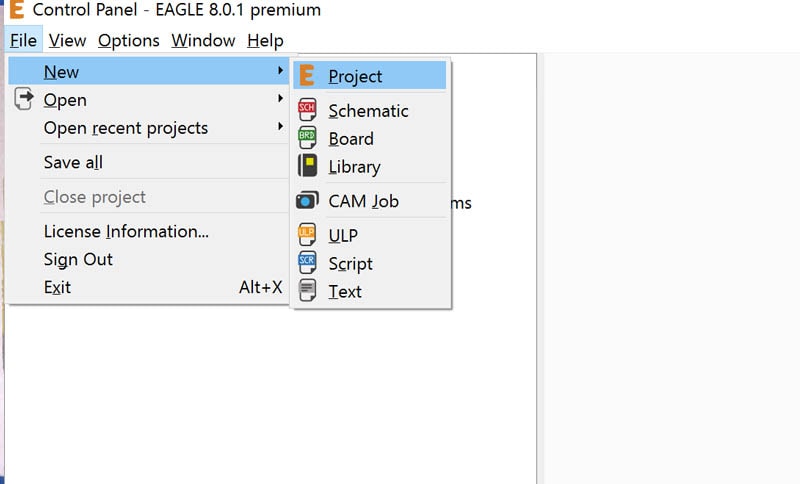
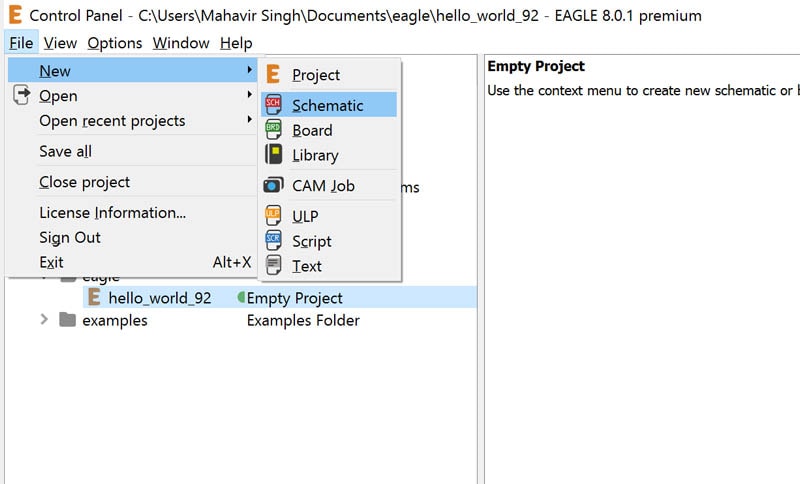
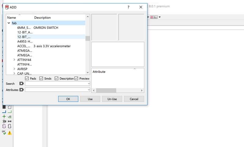
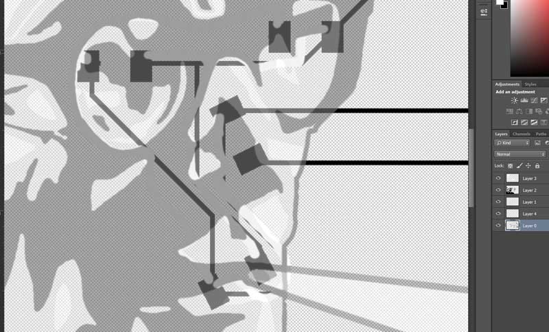
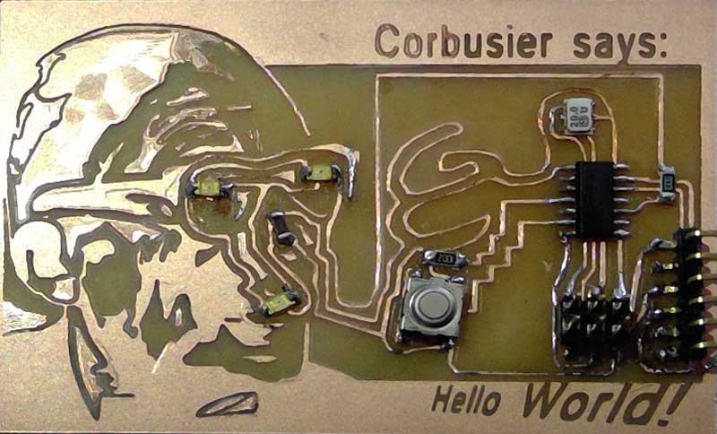
To help myself with connections, I put all three images i need to do the wiring together as a single pic.
Project Files for Week 6
