Week 8: Embedded Programming
Assignment:
- Read a microcontroller data sheet .
- Program your board to do something, with as many different programming languages and programming environments as possible.
- Optionally, experiment with other architectures
This week I have to read the datasheet of ATtiny44 and program the microcontroller using usbtiny.
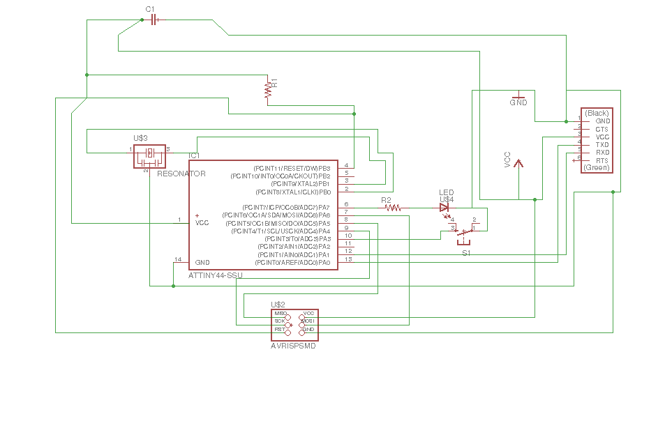
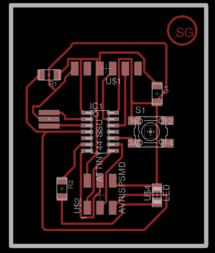
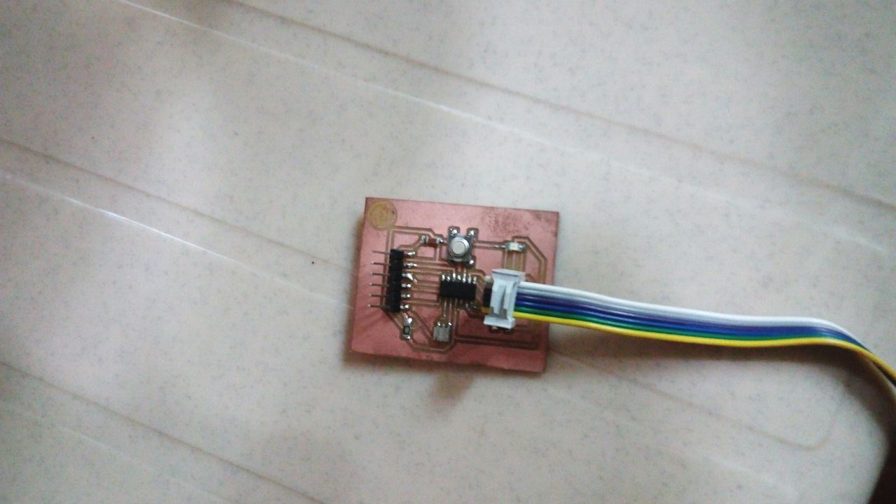
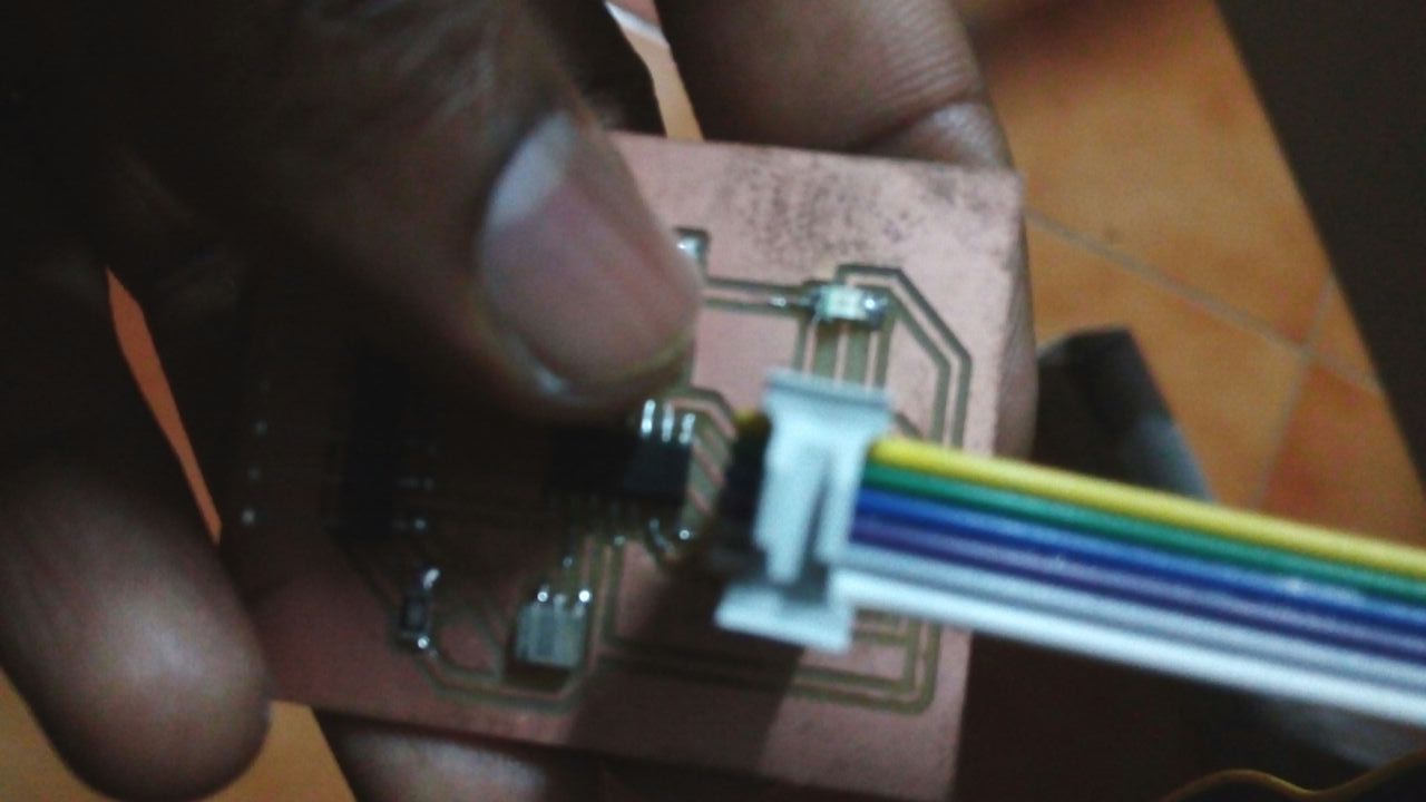
ATtiny44 circuit
In my circuit LED is connected to the pA7 pin and switch is connected to pA3 pin.This can be noticed from the schematic shown below.
|
|
|---|
Programming of ATtiny44
I have a programming experiance with PIC and arduino,with AVR it is my first experiance . As thought by our instructors I came to know that we can use atom as the IDE.In order to compile and flash to the ATtiny44 using compflash which is developed by our instructer, which provides an user interface developed in python where compiling and flash options are available. Actually inside the UI compile option is done using AVR-GCC and flashing is done using avrdude.
Download complash from here.
In addition we have to install avr-gcc and avrdude for that in the terminal run the following commands,
sudo apt-get install gcc-avr
sudo apt-get install avr-libc
sudo apt-get install binutils-avr
sudo apt-get install avrdude
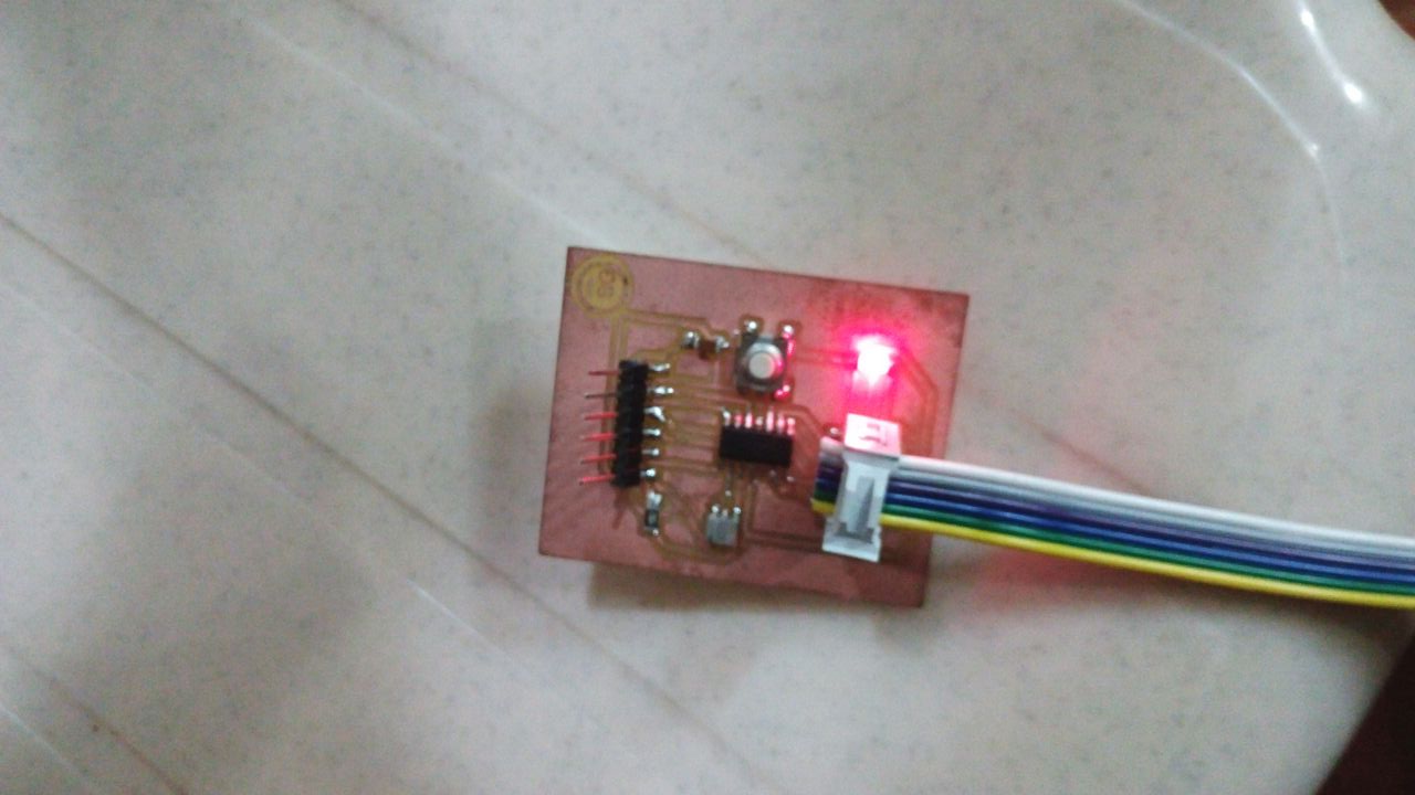
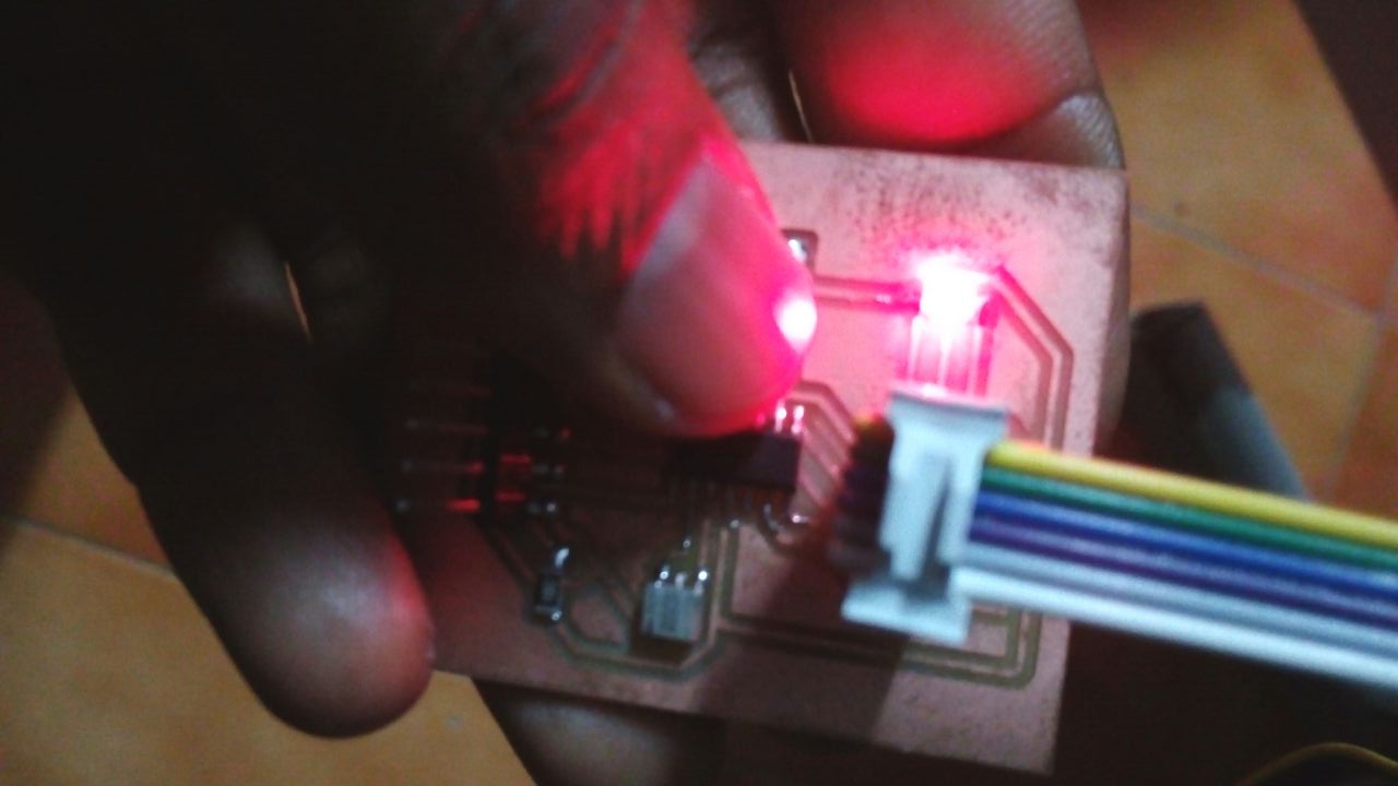
Blink the LED
A program to blink the Led continuesly with time gap of 1 second

in order to compile and flash the program go inside the folder compflash and open the terminal and type
python compflash.py

the User interface will be opened

click on compile after selecting the appropriate file ,controller,programmer

click flash inorder to burn the program into the microcontroller
Note:But we have to cross check the fuse setting ,by clicking the fuse and then click read and I noticed that low fuse value is 5e

In addition to this I noticed that the led is blinking slowly ,ie it is not one second so I concluded that 20Mhz is not being used , it is clear from the low fuse value ,I rectified the problem by writing df

so finally LED blink with a time gapof one second
OUTPUT
|
|
|---|
Download the Program file blink.c
LED ON when KEY pressed
In this program led will blink when the key is being pressed

OUTPUT
|
|
|---|
Download the Program file switch.c
LED ON when KEY pressed a multiple of three times
This is a program where the led will be on only after a certain number of press,here I used 3
I feel there is demerit in this program ,ie we have to press with a slow speed otherwise we may not get correct count.I think this can be rectified if we are using interrupt based programming instead of depending on the software based programing.

OUTPUT
Download the Program file led_3press.c
ATtiny44 Datasheet Review
8-Bit Microcontroller with RISC Architecture with Most Single Clock Cycle Execution
– 32 x 8 General Purpose Working Registers
– 4K Bytes of In-System Programmable Program Memory Flash
–56 Bytes of In-System Programmable EEPROM
–256 Bytes of Internal SRAM
Peripheral Features
– One 8-Bit and One 16-Bit Timer/Counter with Two PWM Channels, Each
– 10-bit ADC
– Programmable Watchdog Timer with Separate On-chip Oscillator
– On-chip Analog Comparator
– Universal Serial Interface
Special Microcontroller Features
– debugWIRE On-chip Debug System
– In-System Programmable via SPI Port
– Internal and External Interrupt Sources
– Enhanced Power-on Reset Circuit
– Programmable Brown-out Detection Circuit
– Internal Calibrated Oscillator
Interrupts
Interrupt mechanism is an important concept while working with microcontroller,so lets have a breif introduction.Figure given below shows the pin diagram of ATtiny44.

The External Interrupts are triggered by the INT0 pin or any of the PCINT11:0 pins even if the INT0 or PCINT11:0 pins are configured as outputs,thus provides a way for generating software Interrupts. Pin change 0 interrupts PCI0 will trigger if any enabled PCINT7:0 pin toggles. Pin change 1 interrupts PCI1 will trigger if any enabled PCINT11:8 pin toggles.

The INT0 interrupts can be triggered by a falling or rising edge or a low level.A low level interrupt on INT0 is detected asynchronously. This means that the interrupt source can be used for waking the part also from sleep modes other than Idle
Registers used for Interrupt handling
SREG – AVR Status Register

Bit 7 – I: Global Interrupt Enable The Global Interrupt Enable bit must be set for the interrupts to be enabled. The individual inter- rupt enable control is then performed in separate control registers. If the Global Interrupt Enable Register is cleared, none of the interrupts are enabled independent of the individual interrupt enable settings. The I-bit is cleared by hardware after an interrupt has occurred, and is set by the RETI instruction to enable subsequent interrupts. The I-bit can also be set and cleared by the application with the SEI and CLI instruction.,/p>
The interrupt execution response for all the enabled AVR interrupts is four clock cycles mini- mum. After four clock cycles the Program Vector address for the actual interrupt handling routine is executed. During this four clock cycle period, the Program Counter is pushed onto the Stack. The vector is normally a jump to the interrupt routine, and this jump takes three clock cycles. If an interrupt occurs during execution of a multi-cycle instruction, this instruction is completed before the interrupt is served. If an interrupt occurs when the MCU is in sleep mode, the interrupt execution response time is increased by four clock cycles. This increase comes in addition to the start-up time from the selected sleep mode. A return from an interrupt handling routine takes four clock cycles. During these four clock cycles, the Program Counter (two bytes) is popped back from the Stack, the Stack Pointer is incremented by two, and the I-bit in SREG is set.
GIMSK – General Interrupt Mask Register

Bit 6 – INT0: External Interrupt Request 0 Enable
When the INT0 bit is set (one) and the I-bit in the Status Register (SREG) is set (one), the exter-
nal pin interrupt is enabled. The Interrupt Sense Control bits (ISC01 and ISC00) in the External
Interrupt Control Register A (EICRA) define whether the external interrupt is activated on rising
and/or falling edge of the INT0 pin or level sensed. Activity on the pin will cause an interrupt
request even if INT0 is configured as an output. The corresponding interrupt of External Interrupt
Request 0 is executed from the INT0 Interrupt Vector.
Bit 5 – PCIE1: Pin Change Interrupt Enable 1 When the PCIE1 bit is set (one) and the I-bit in the Status Register (SREG) is set (one), pin change interrupt 1 is enabled. Any change on any enabled PCINT11:8 pin will cause an inter- rupt. The corresponding interrupt of Pin Change Interrupt Request is executed from the PCI1 Interrupt Vector. PCINT11:8 pins are enabled individually by the PCMSK1 Register.
Bit 4 – PCIE0: Pin Change Interrupt Enable 0 When the PCIE0 bit is set (one) and the I-bit in the Status Register (SREG) is set (one), pin change interrupt 0 is enabled. Any change on any enabled PCINT7:0 pin will cause an interrupt. The corresponding interrupt of Pin Change Interrupt Request is executed from the PCI0 Inter- rupt Vector. PCINT7:0 pins are enabled individually by the PCMSK0 Register.
MCUCR – MCU Control Register

Bits 1:0 – ISC01, ISC00: Interrupt Sense Control 0 Bit 1 and Bit 0
The External Interrupt 0 is activated by the external pin INT0 if the SREG I-flag and the corre- sponding interrupt mask are set. The level and edges on the external INT0 pin that activate the interrupt are defined in Table given. The value on the INT0 pin is sampled before detecting edges. If edge or toggle interrupt is selected, pulses that last longer than one clock period will generate an interrupt. Shorter pulses are not guaranteed to generate an interrupt. If low level interrupt is selected, the low level must be held until the completion of the currently executing instruction to generate an interrupt.

PCMSK1 – Pin Change Mask Register 1
Bits 7:4 – Res: Reserved Bits and will always read as zero.
Bits 3:0 – PCINT11:8: Pin Change Enable Mask 11:8
Each PCINT11:8 bit selects whether pin change interrupt is enabled on the corresponding I/O
pin. If PCINT11:8 is set and the PCIE1 bit in GIMSK is set, pin change interrupt is enabled on
the corresponding I/O pin. If PCINT11:8 is cleared, pin change interrupt on the corresponding
I/O pin is disabled.

PCMSK0 – Pin Change Mask Register 0
Bits 7:0 – PCINT7:0: Pin Change Enable Mask 7:0 Each PCINT7:0 bit selects whether pin change interrupt is enabled on the corresponding I/O pin. If PCINT7:0 is set and the PCIE0 bit in GIMSK is set, pin change interrupt is enabled on the cor- responding I/O pin. If PCINT7:0 is cleared, pin change interrupt on the corresponding I/O pin is disabled.

GIFR – General Interrupt Flag Register

Bits 7, 3:0 – Res: Reserved Bits
These bits are reserved in the ATtiny24/44/84 and will always read as zero.
Bit 6 – INTF0: External Interrupt Flag 0
When an edge or logic change on the INT0 pin triggers an interrupt request, INTF0 becomes set
(one). If the I-bit in SREG and the INT0 bit in GIMSK are set (one), the MCU will jump to the cor-
responding Interrupt Vector. The flag is cleared when the interrupt routine is executed.
Alternatively, the flag can be cleared by writing a logical one to it. This flag is always cleared
when INT0 is configured as a level interrupt.
Bit 5 – PCIF1: Pin Change Interrupt Flag 1
When a logic change on any PCINT11:8 pin triggers an interrupt request, PCIF1 becomes set
(one). If the I-bit in SREG and the PCIE1 bit in GIMSK are set (one), the MCU will jump to the
corresponding Interrupt Vector. The flag is cleared when the interrupt routine is executed. Alter-
natively, the flag can be cleared by writing a logical one to it.
Bit 4 – PCIF0: Pin Change Interrupt Flag 0
When a logic change on any PCINT7:0 pin triggers an interrupt request, PCIF becomes set
(one). If the I-bit in SREG and the PCIE0 bit in GIMSK are set (one), the MCU will jump to the
corresponding Interrupt Vector. The flag is cleared when the interrupt routine is executed. Alter-
natively, the flag can be cleared by writing a logical one to it.
KEY PRESS using Interrupt mechanism

This program is same as the previous,key press only difference is Pin change interrupt request is being used.
The response is quick compared to previous one
Download the Program file intc.c