Week 4: Electronics Production
Assignment:
- Make an in-circuit programmer by milling the PCB
- Optionally, trying other processes
This week my assignment is to make an in-circuit programmer using ATtiny45 microcontroller..
In-circuit Programmer
In-system programming (ISP), also called In-Circuit Serial Programming (ICSP), is the ability of some programmable logic devices, microcontrollers, and other embedded devices to be programmed while installed in a complete system, rather than requiring the chip to be programmed prior to installing it into the system. The need of in-circuit programmer is due to the fact that ,there are no programming sockets for small package chips and Its a pain to move chips in and out of the programmer during development,which is Impossible for surface mount parts. The Tiny AVR Programmer can directly program almost all AVR (including the ATmega328 and ATmega32U4) whether they are on Arduino boards or in a breadboard.
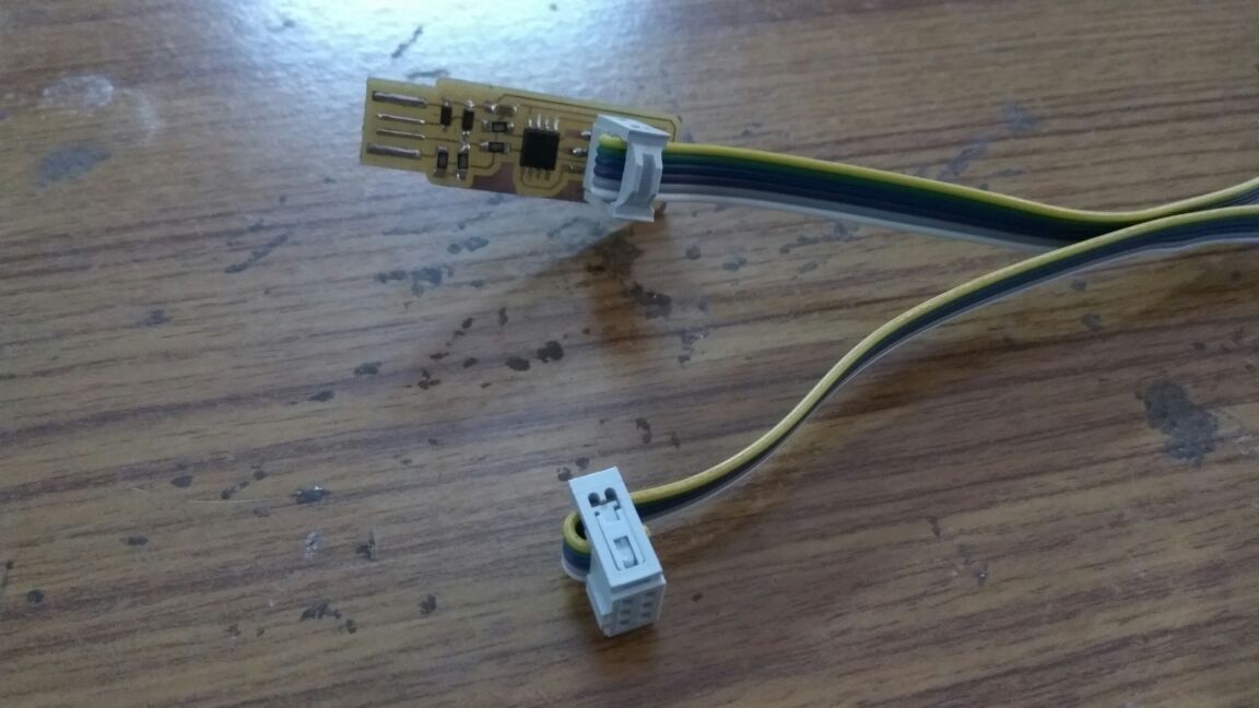
FabTinyISP
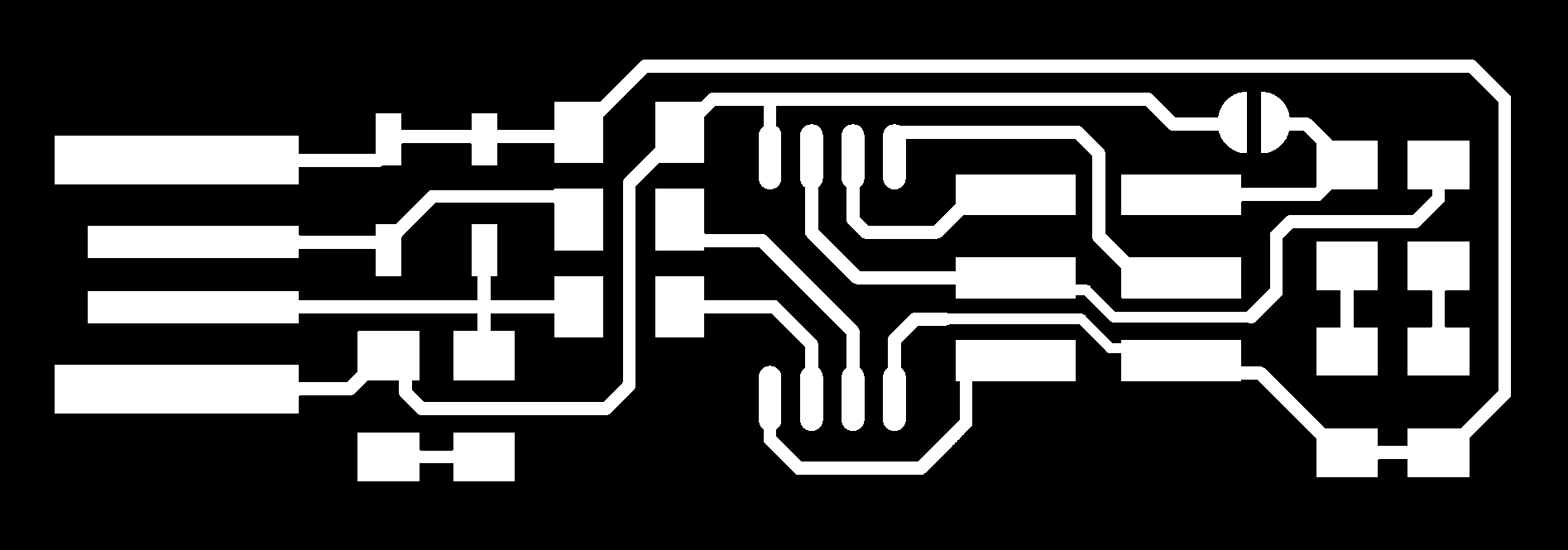
I selected Brians version of Fab ISP.The circuit diagram and the pcb design is given below.
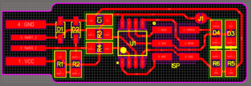
|
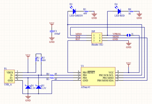
|
|---|---|
| Board image | schematic diagram |
ATtiny45
In our Fab ISP we are using ATtiny45 microcontroller.ATtiny45 is a low-power CMOS 8-bit microcontroller which is based on the AVR enhanced RISC architecture.
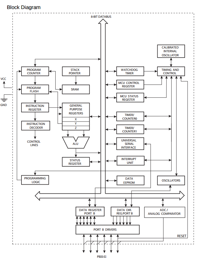
The AVR core combines a rich instruction set with 32 general purpose working registers. All 32 registers are directly connected to the Arithmetic Logic Unit (ALU), allowing two independent registers to be accessed in one single instruction executed in one clock cycle. The resulting architecture is more code efficient while achieving throughputs up to ten times faster than conventional CISC microcontrollers.
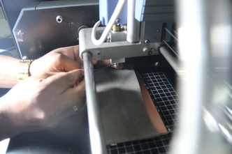
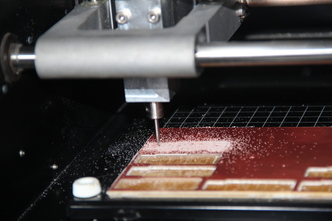
Milling with Roland Modella MDX-20
MODELA Player quickly imports our design which is in png format and prepares for milling. In order to start operation , set the model's scale and milling direction from the tool and material libraries in the software. Next, select the size and type of materials to be milled. MODELA Player automatically sets the best milling parameters based on the materials you choose. Then click start. our ideas are quickly transformed into reality.
|
|
|---|---|
| Work plate and Sacrificial Layer | PCB |
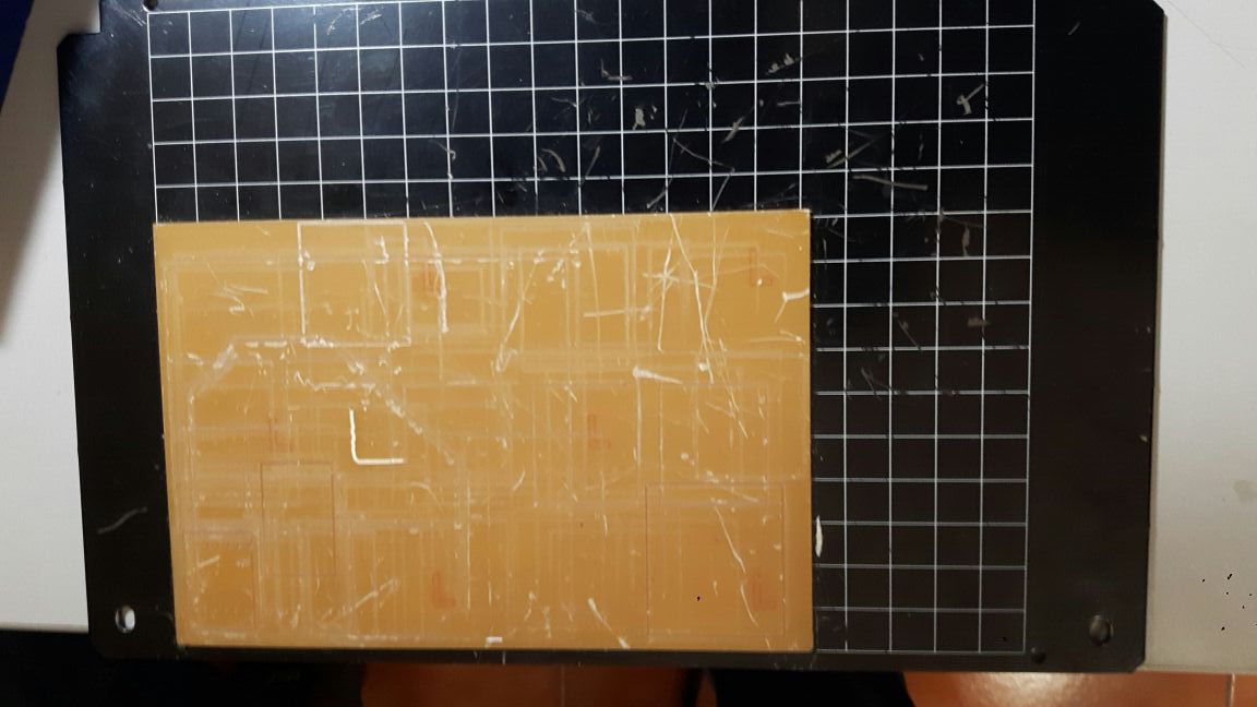
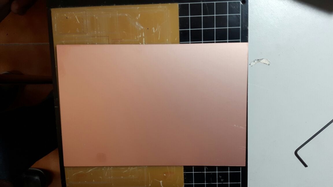
Before the process of milling,inorder to protect end mill it is mandatory to place the pcb over the Sacrificial Layer , which should be further kept on the work plate.
|
|
|
|---|
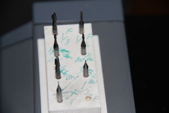
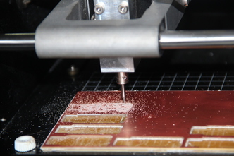
PCB milling is done using following two bits:
1/64 in- This end mill is used to remove the copper layer from the board.
1/32 in- This end mill is used to cut out the PCB from the mother board.
The most important procedure is to place the end mill in the tool head,it should be done with care.
In order to do that
first we have to go for the Fab module settings

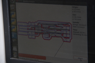
Type fab in command prompt and in the menu box select png image format and Roland MDX 20-mill and click on make_png_rmls

select mill traces(1/64) inorder to remove the copper layer.1/64 represents 0.4mm diameter of the end mill

load the image of the traces which had to milled .
Download my design file traces

click on make_path and we will get the vector diagrom of the image loaded

click on make.rml

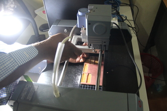
click on send it,but before doing so we must be sure about the position of the tool head ,for that we have to change the xmin and ymin value and click on move to xmin,ymin .now the machine will position our tool head to required point from where milling should begin.After we are sure about the position , send it button can be pressed.Now the control will be transfered to the machine and it starts the process of milling.A modela output window will appear , where the red lines represents the milling traces completed.


|
|
|
|---|
After milling process is over we have to click view mode in the machine so that we can take the milled pcb outside.
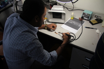
Soldering
This is the hardest part ,it requires so much patience and skill.I felt difficult while soldering, but i am so much intrested to study soldering , at last i could do it .I was very happy.
|
|
|---|
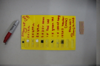
The components used are given in the above figure.In the case of soldering process,Tip maintenance is
an important step in keeping your Iron and tips in working order and maximizing the use of them, it is important to keep
it clean and when stored always keep a nice blob of solder on the working edges of the tip.
The steps I used while soldering is given below
Step 1 --> Place a small amount of solder on one of the two pads. Aprox. 0.5mm in height.
Step 2 -->Grab the electronic part(resistor,capacitor,microcontroller etc) with very fine tweezers. Bring the part overtop of
the pads, slight to one side so that the part can sit flat against the PCB.
Heat the pad already with solder and slide the part onto the pad so that it is centered between the pads. Remove heat.
Step 3--> Put a small force down on the part and re-heat the one pad to guarantee that the parts is flat against the PCB.
Step4-->Solder the other side of the part.
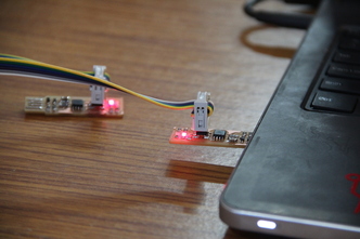
Fab ISP programming
|
|
|---|
My Fab ISP is programed using the link here

In order to confirm that my Fab ISP is functioning properly , I connected my device to pc and checked its connectivity ,using the command "lsusb" in command terminal.