Specific material and softwares used during this assignment
- CNC mill 0.1mm, 0.4mm and 2mm
- Components :
- 1 ATtiny44
- 1 FTDI 3.3-5V
- 1 6 pin header
- 1 Crystal 20 MHz (resonator)
- 1 Resistor 4.7K (standard value in case of doubt)
- 1 Resistor 330 ohm (red led)
- 1 Resistor 280 ohm (green led)
- 1 Capacitor 1 uF
- 1 Capacitor 27 pF (crystal)
- 1 Capacitor 27 pF (crystal)
- 1 LED Red
- 1 LED green
- 1 push button
- Software :
- FlatCam
- KiCad
- Electrodroid
Designing of the board
A friend of mine gave me a quick crash-course on Kicad so I will be using this software for the design
I have found a kicad library wit the fabacademy components here
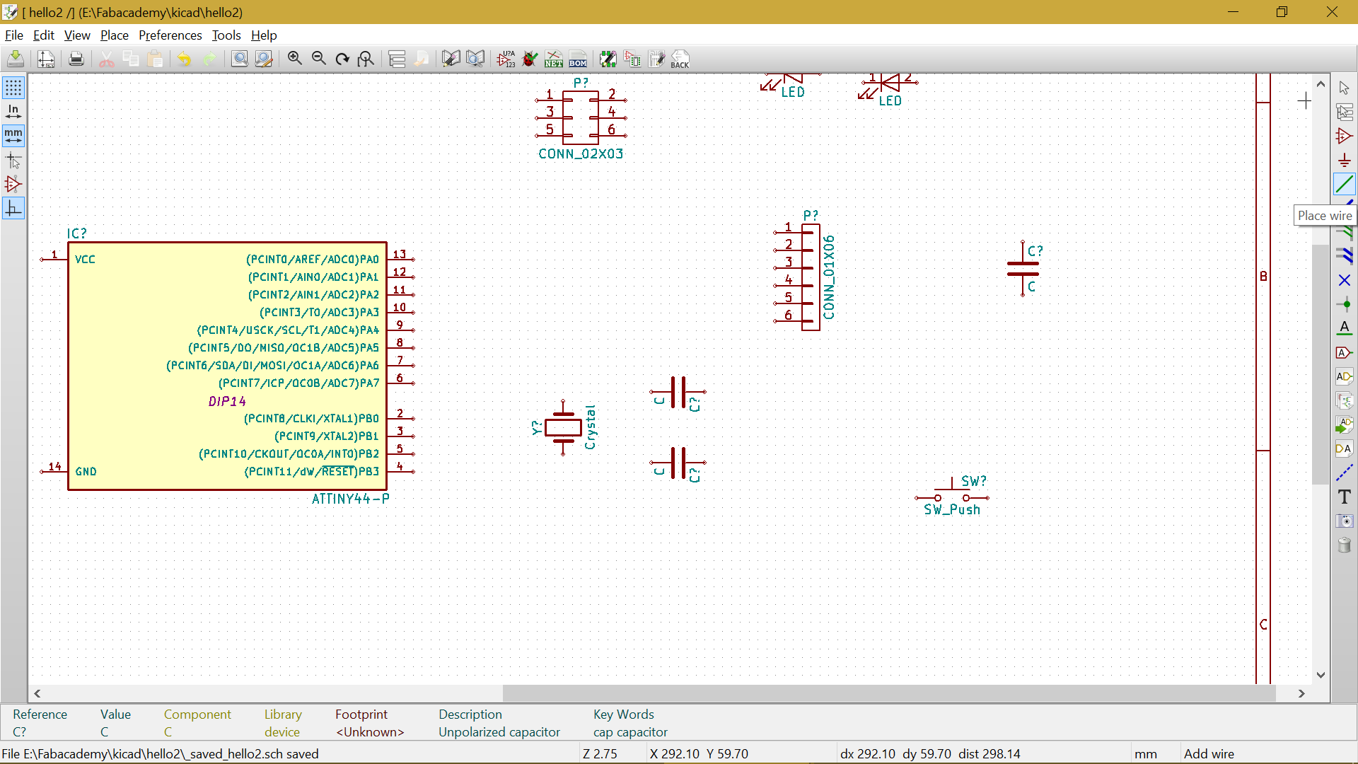
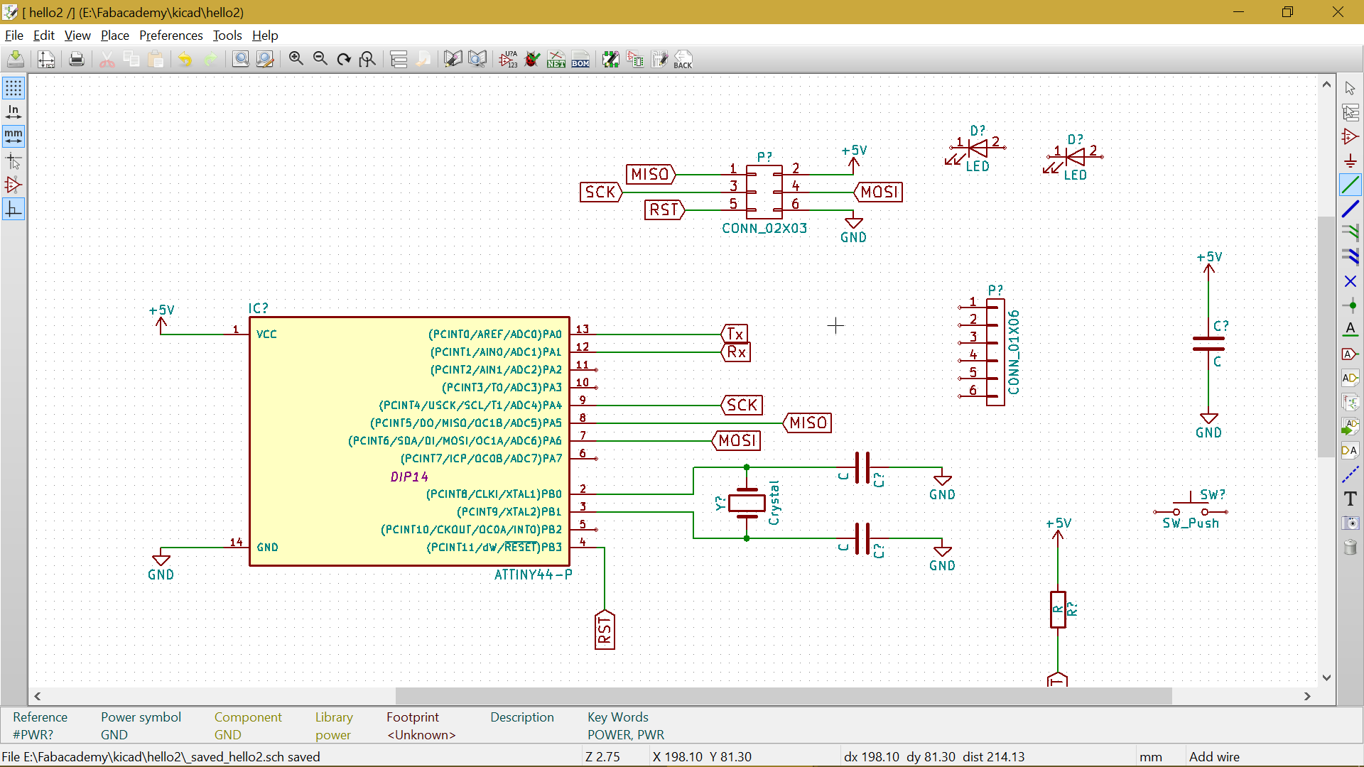
I have then attacked the schematic as you can see in the images below :
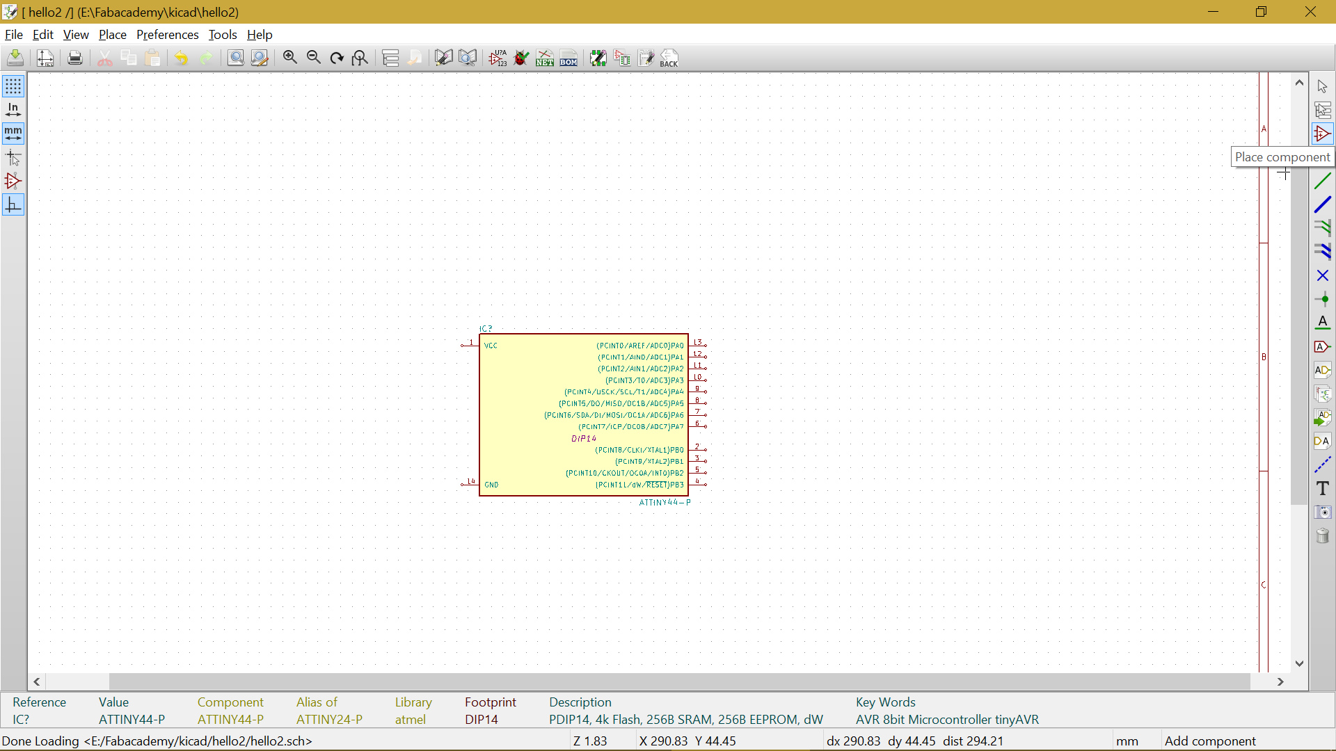
To place a component, you just need to push the "place component" button on the right panel and click into your schematic
A new window will pop-up will all the components available in Kicad and the loaded library. A simple search give me quickly my Attiny44-P. I have done the same operartion for all the components
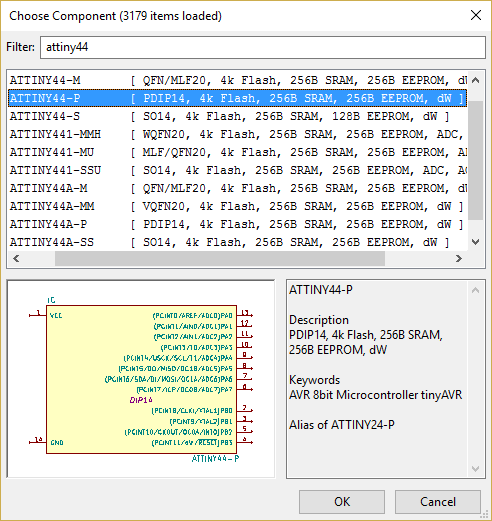
I have quickly discovered that the switch we need as push-button is not there by default. I have simply loaded the switch library to solve the issue
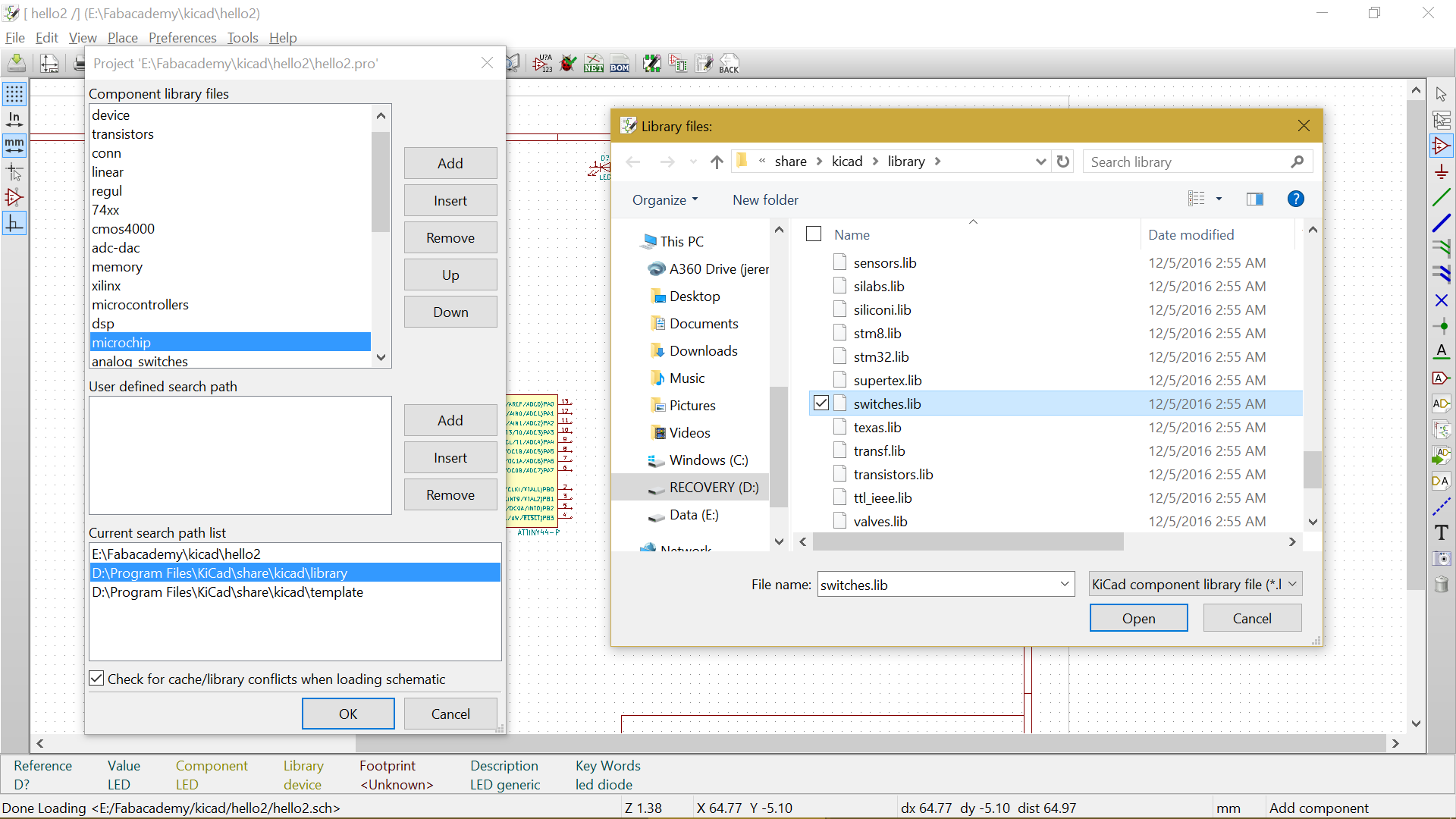
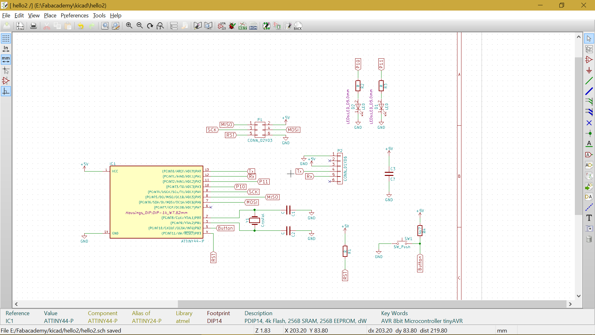
You can see almost all the components needed for this assignment before wiring
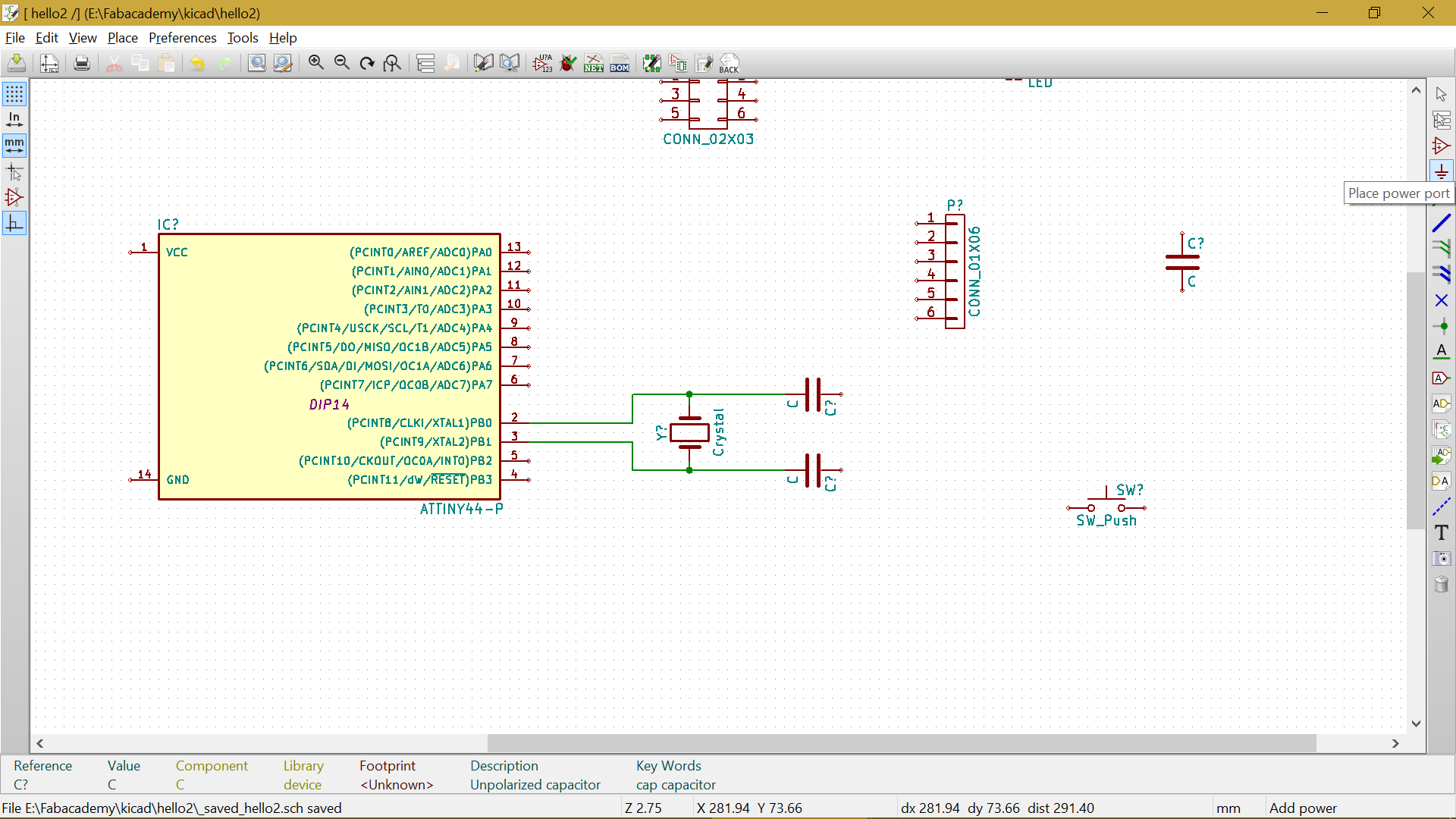
Now the real fun begins with the "place wire" button on the right panel and click into your schematic/component
I have started with the crystal, it need to be connected to the pin 2 and 3 of the Attiny44 and two capacitors must be added
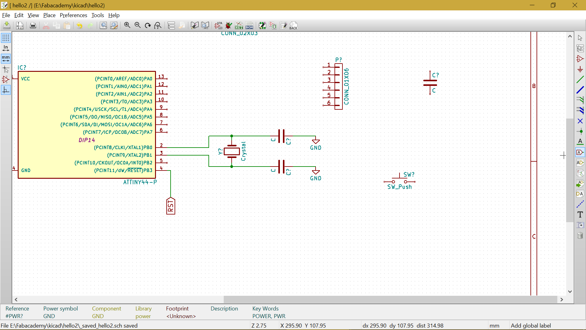
I moved next to the pin 4/reset and the use of Global Label. You can place them with the "place global labe" button on the righ panel. They are really useful as the allow you connect a component without apparent wires. Your schematic stays clear and you can easily read what is connected to a component
Thanks to the label "RST" I have connected the pin 4 to a resistor and the +5V without apparent wiring
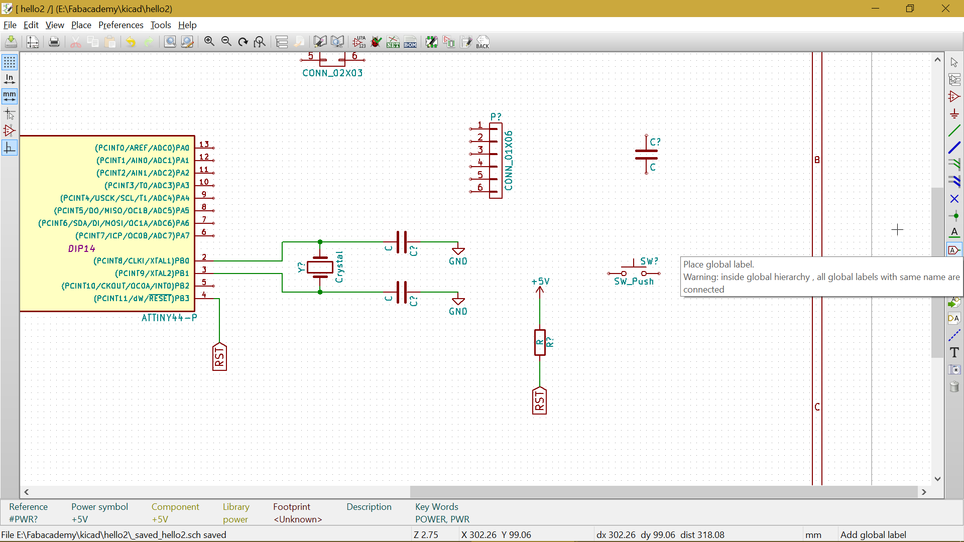
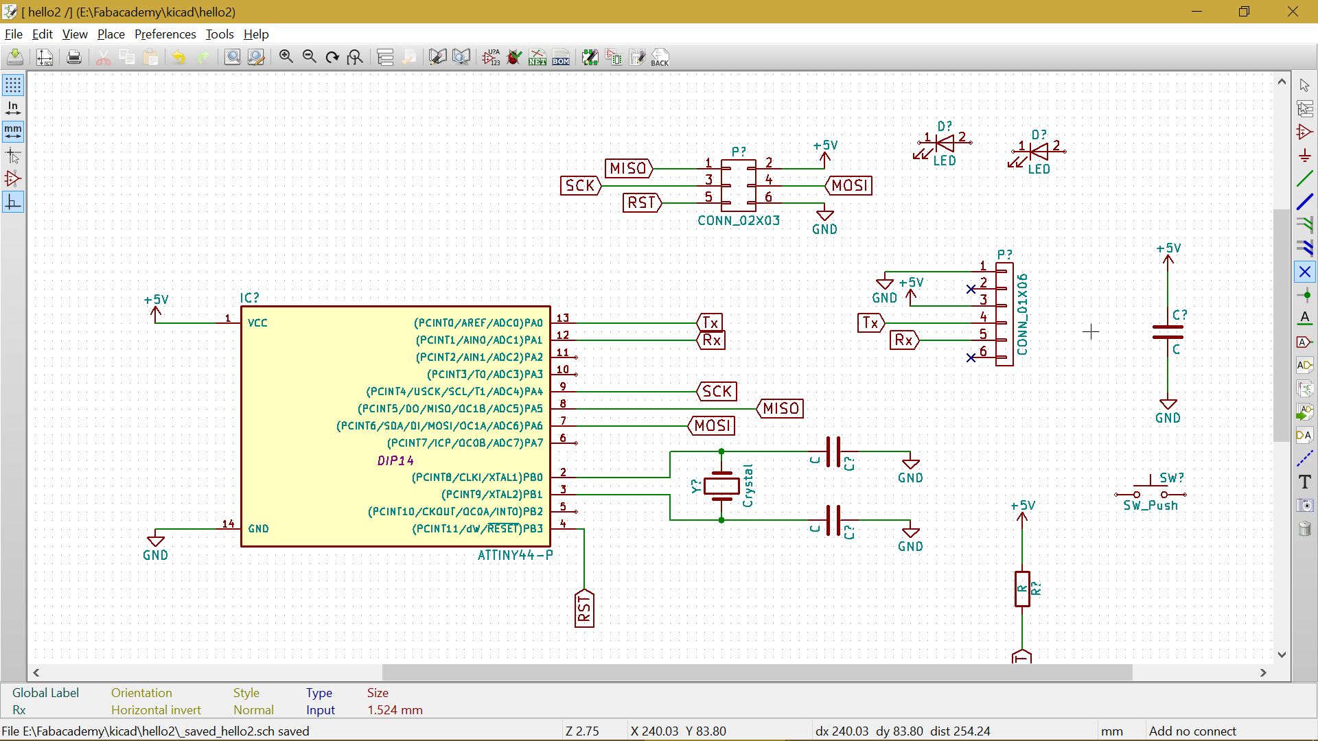
I have continued with the label to connect the right pins of the ATtiny to the connectors, all thanks to the pinouts found online
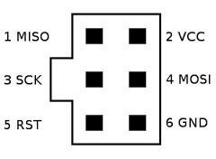
The ISP Pinouts
The two connectors are now linked via labels to the Attiny
The FTDI Pinouts
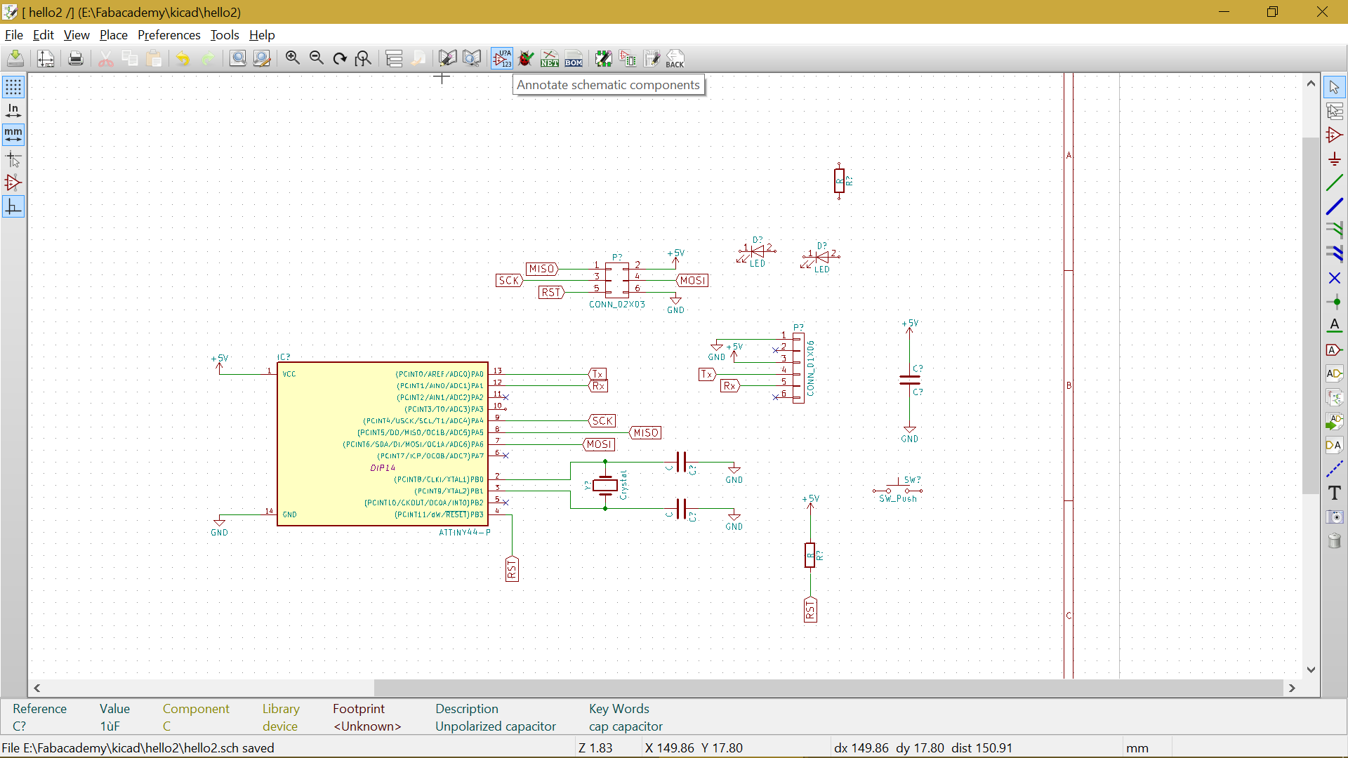
Almost done, time to make some checks and annotations
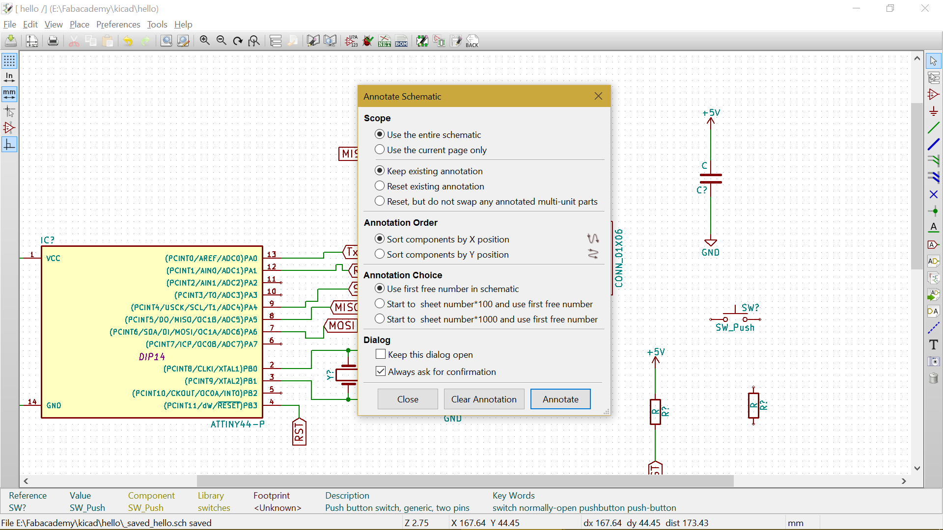
I have now annoted the schema thanks to the "annotate schematic components" button, located on the top bar. It means that every components will have a reference and number (all my resistors have now number R1,R2,...). Kicad needs to make all necessary checks and association
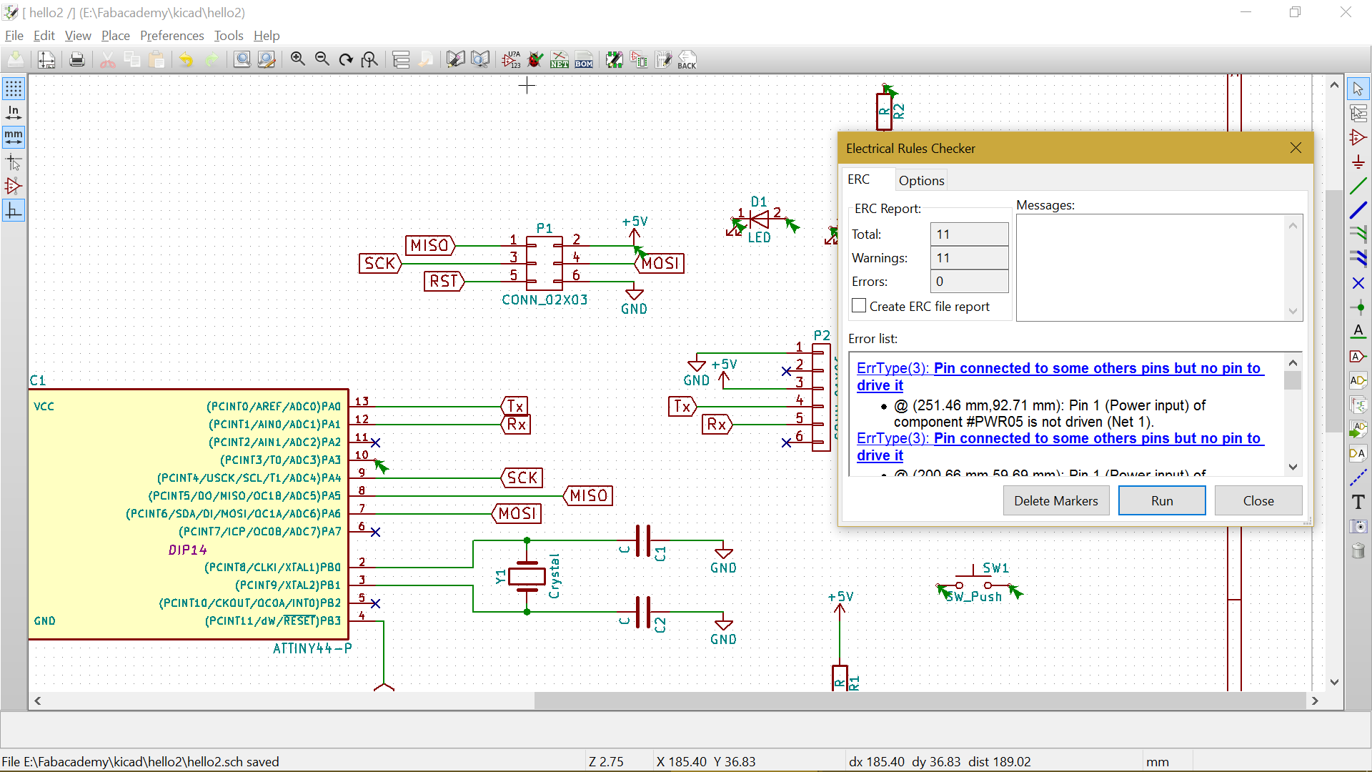
Once my components are annoted, i can make a quick electric rule check thanks to the "electrical rule check" button (on the top, look like a bug). It checks if all my connectors and components are correctly connected. Really useful to check your circuit. It place markers everywhere you have an issue and a simple click on the hyperlink in the window bring you to the issue (mine is not yet finished but stil useful to do it time to time)
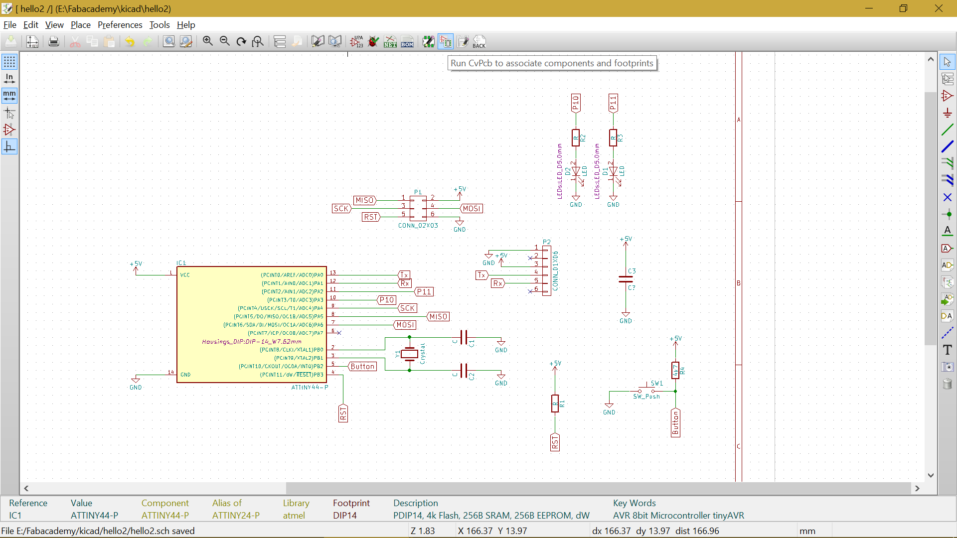
Everything I need is now on the schematic, time to link it to the right footprint
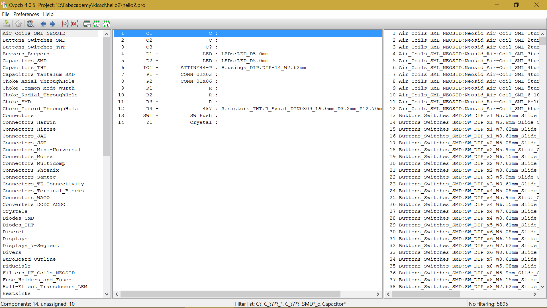
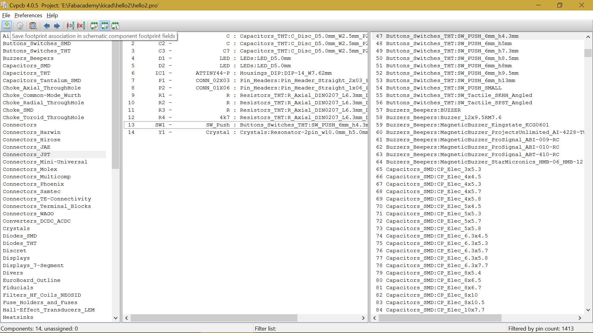
In order to do that, we will used the CvPCB button on the top and load the components libraries
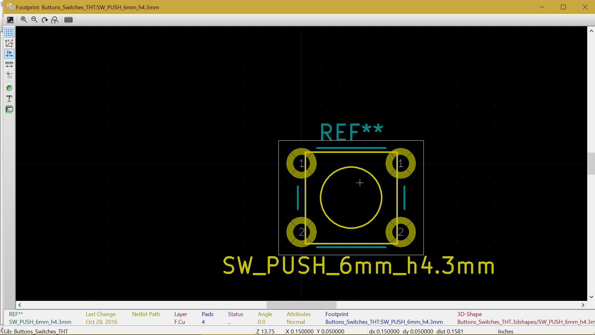
Some components are already recognized as I have indicated in their properties the correct value in the previous phase. You can see on the right the left the different categories of components, on the right the several flavours (physical) of each categories and on the middle, all the compoents of your schematic you need a physical footprint. We need to tell Kicad what kind of components we will use on the PCB(Pitch, diameter, packaging,...)
You can see for each component his physical representation for Kicad (and in reality)
I have choose all my components according to what I have here in the lab
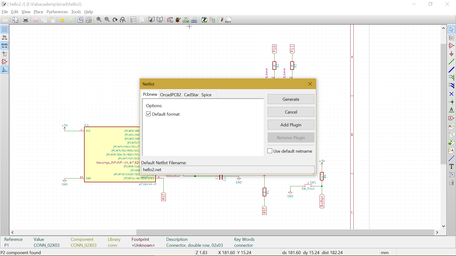
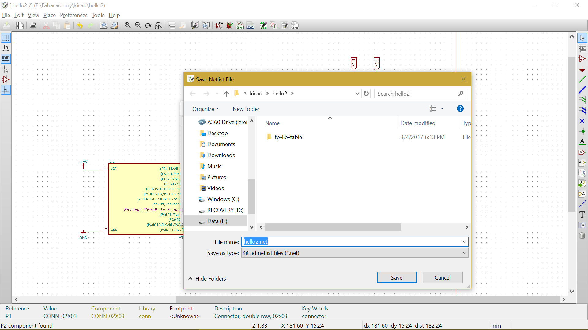
Now you need to come back in the schematic and generate the "netlist" via the button on the top bar. It will create the list with all components and their related footprints
We will save it for later in the folder. It's needed to create the correct PCB
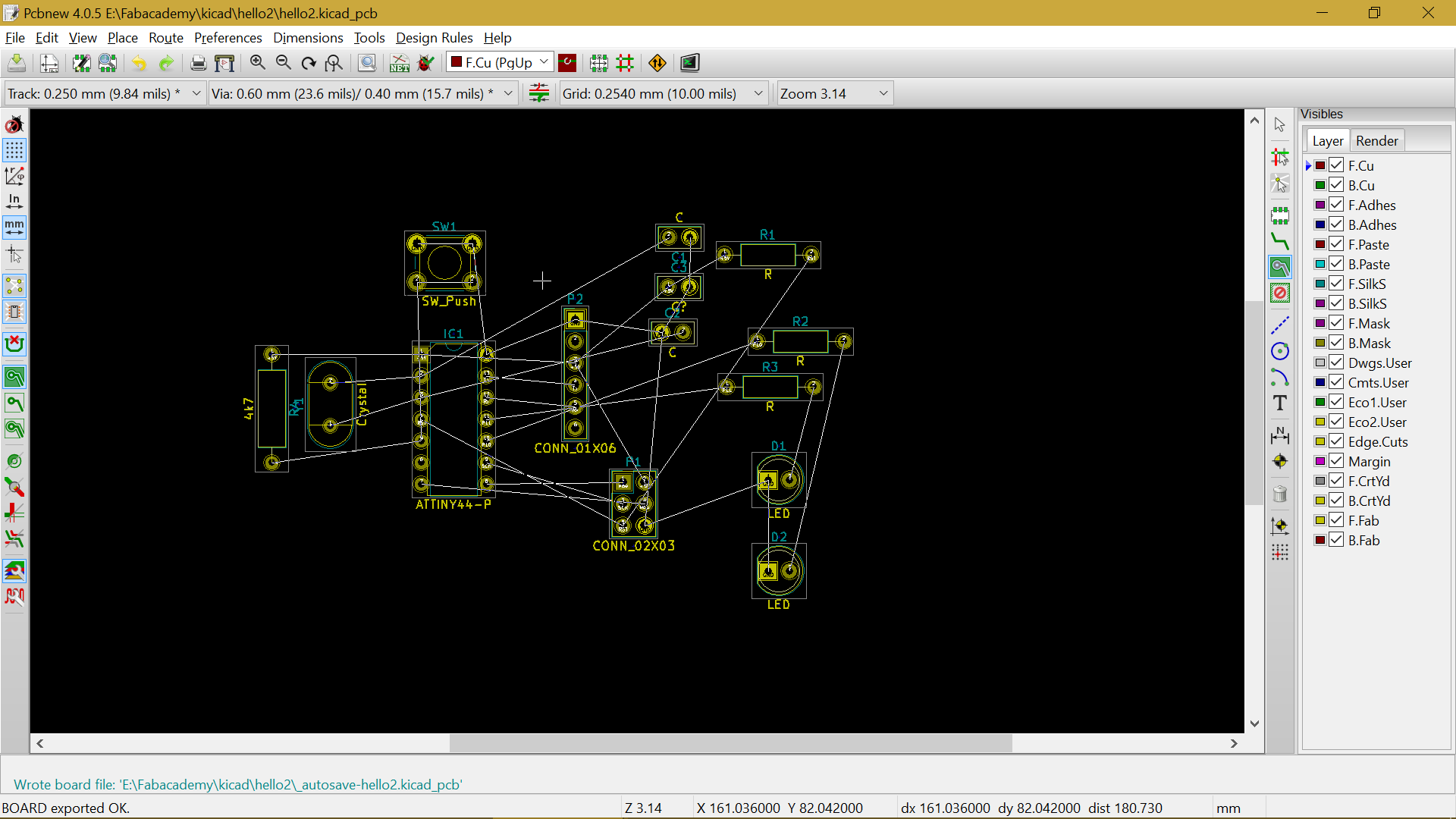
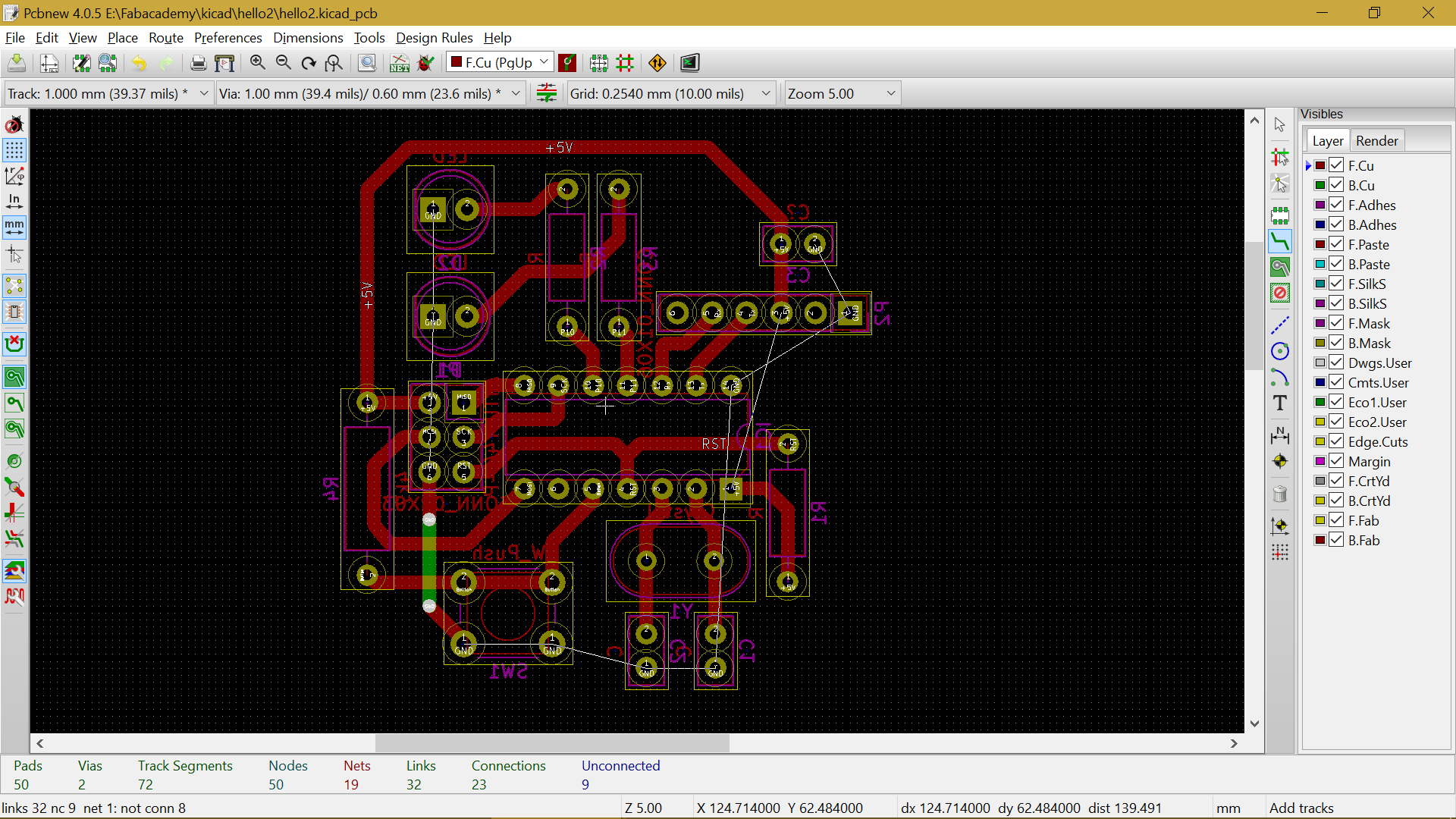
Now we need to open the .pcb created in the beginning by Kicad and import our netlist thanks the same button (but different function here). And Tadaaa! We have a wonderfull tangle of components and connections
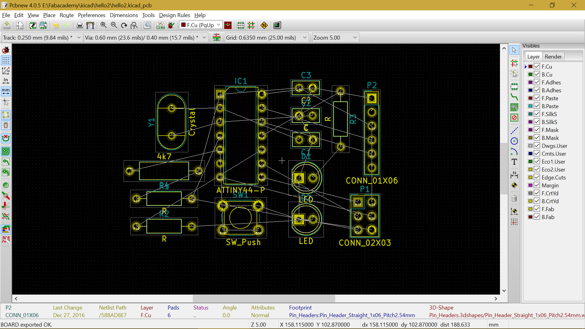
After a few moving around, it's a little better
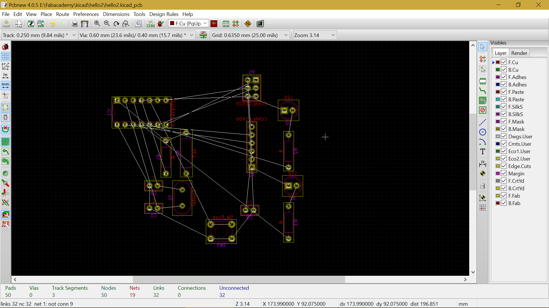
I need now to invert my components as I working with Pdip packaging and milling for the board (Select everything and hit the F letter)
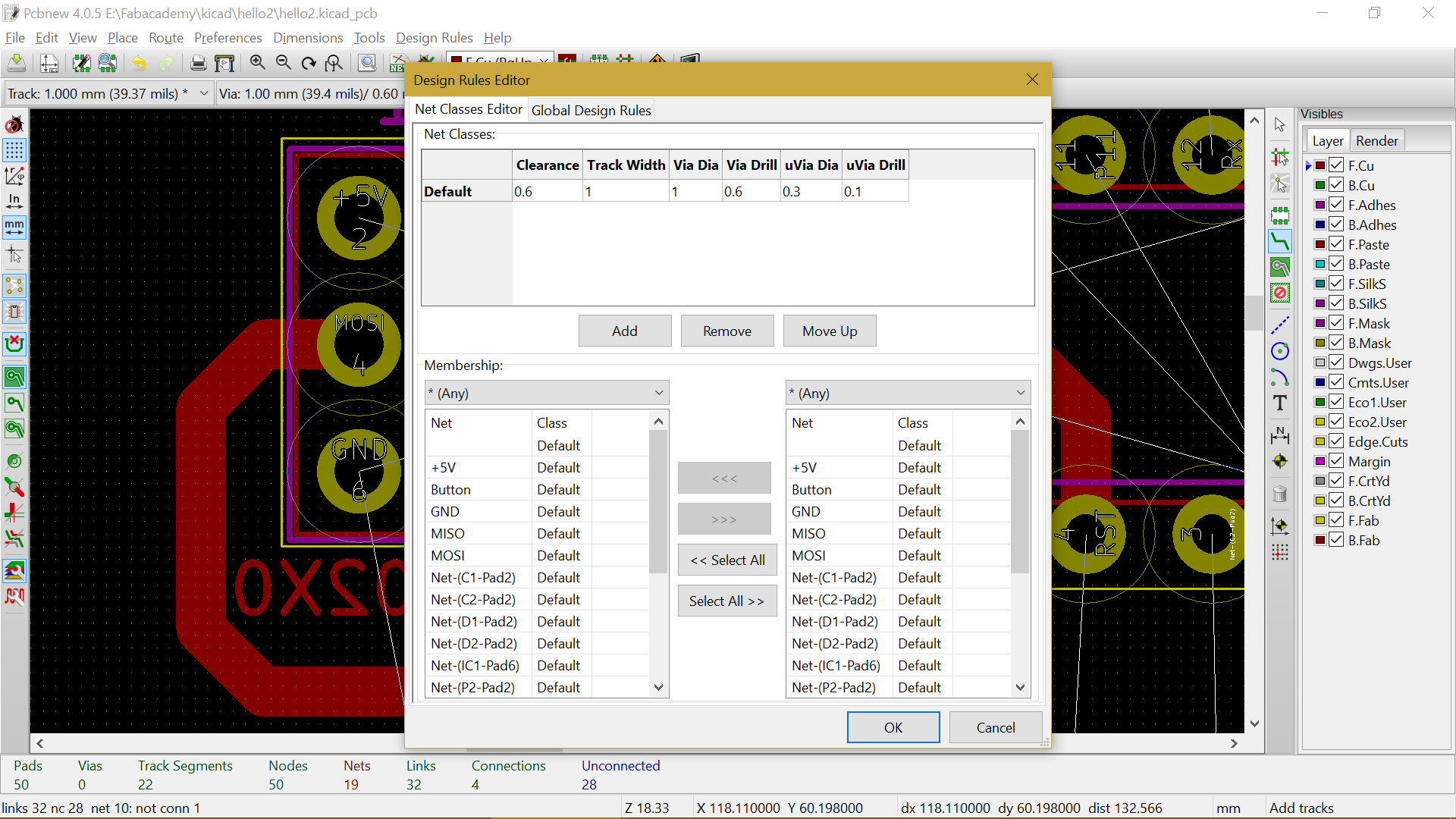
I will go in the design rules (in the top bar) so I can adjust the size of the trace for our CNC and drill bits
The board is looking good, I have simply connected the pads via the traces and my former schematic highlight the pads I need to connect, components by components. The placement is key and not so easy...
The two green traces will be wires, no way (yet) to connect them. I have filled the board with the ground (the copper here), it's easier to connect them all in once. Around it I have traced the Edge Cut, so my board cand be cut from the copper board
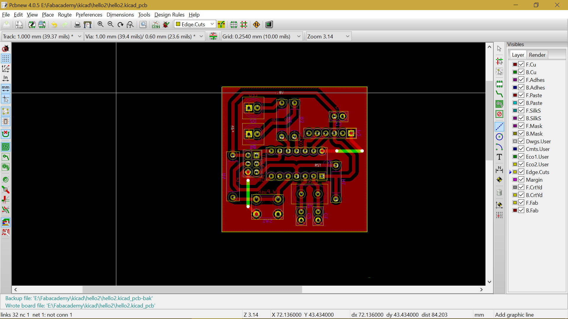
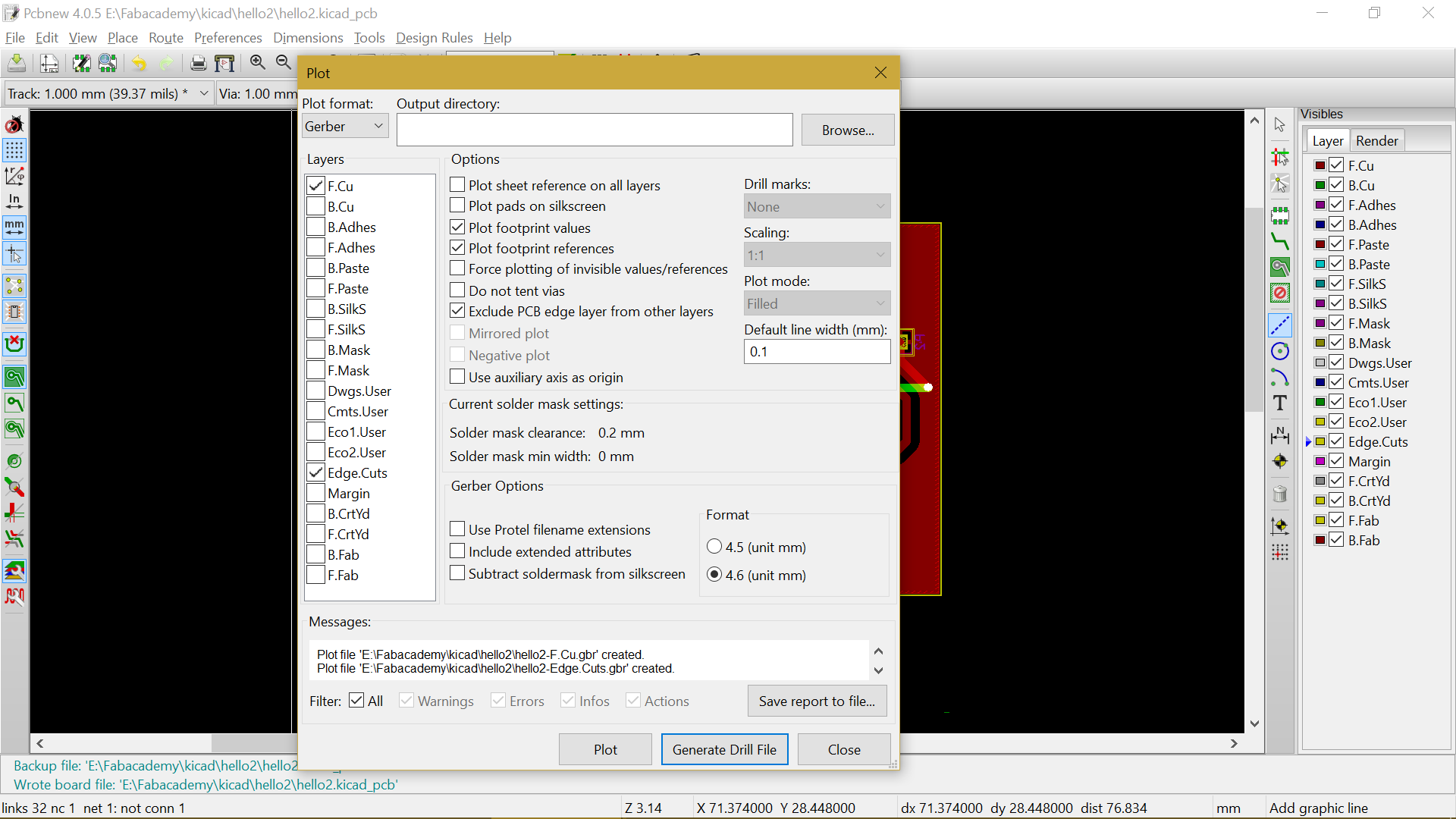
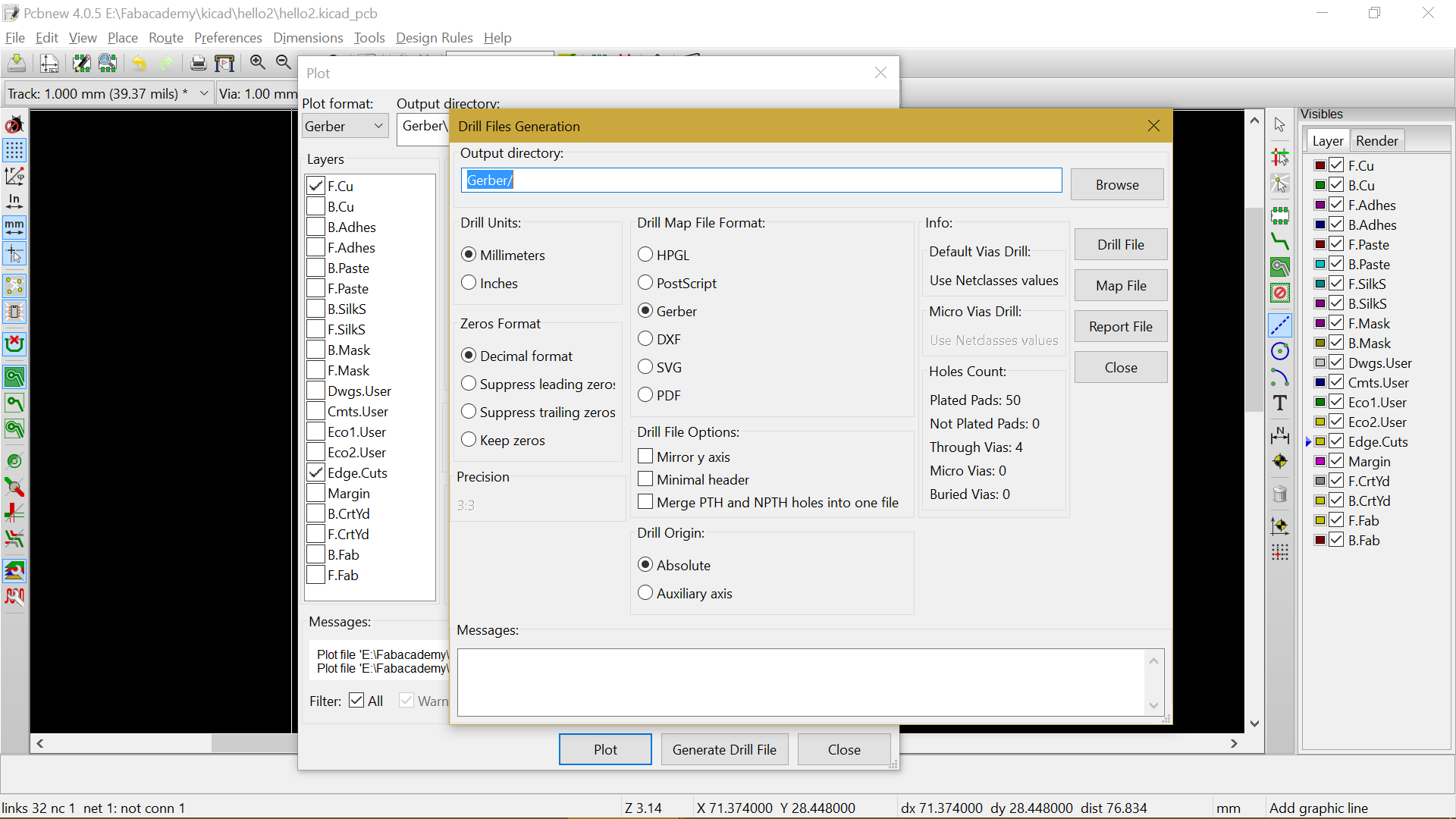
I will now "plot" (File and then the plot button) my PCB in order to mill it. I will need 3 files : the traces, the edge cut and the drill holes. The two first are generated via the plot button, the last one via generate drill file. We have now a correct PCB and the gerber files needed for milling
The screen for the generation of the drill holes file
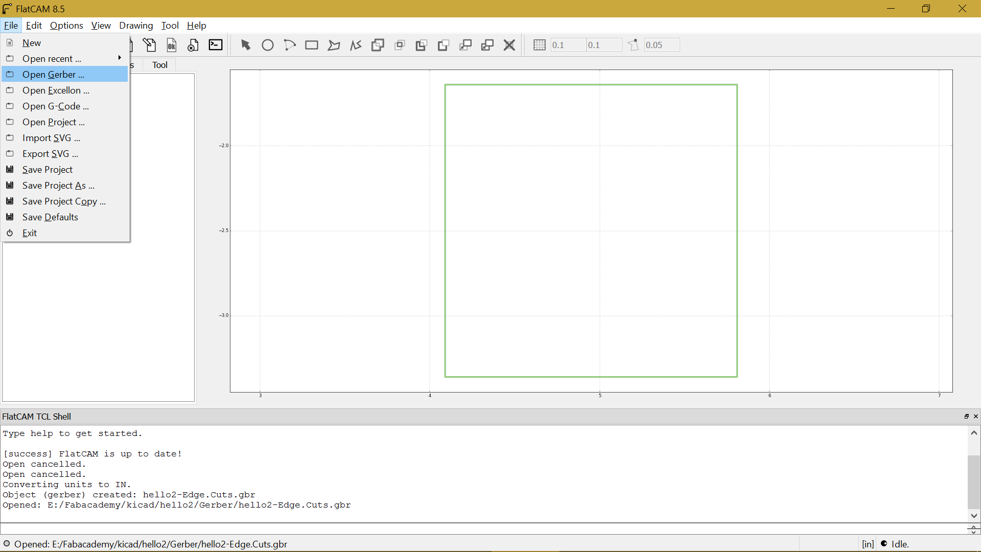
The gerber files generated are correct but I need to translate them and prepare them for our CNC. I will use Flacam for this. The files for the traces and the Edge Cuts are open as Gerber files
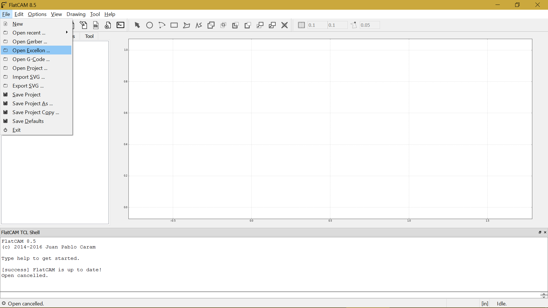
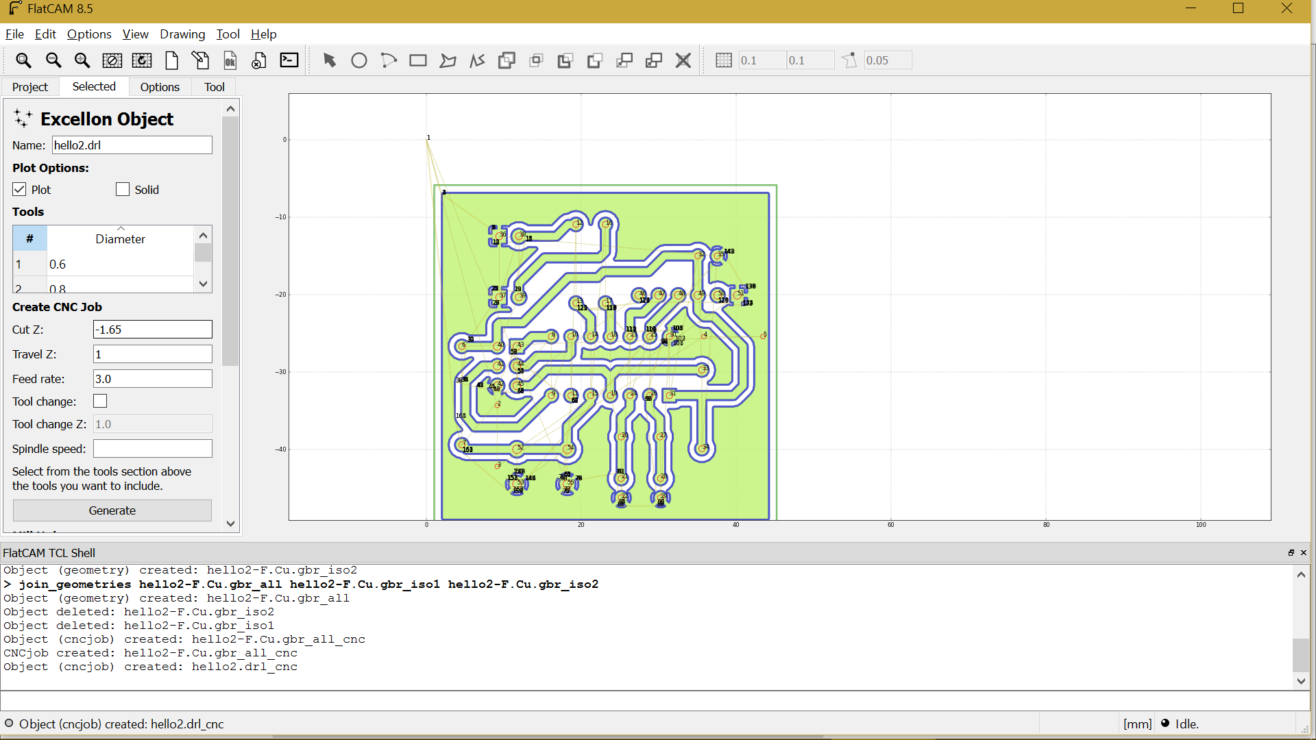
The file with the drill holes need to be open as Excellon
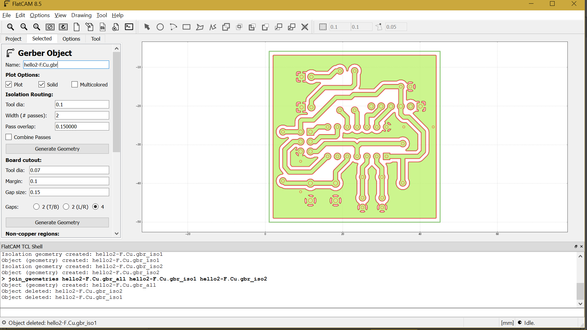
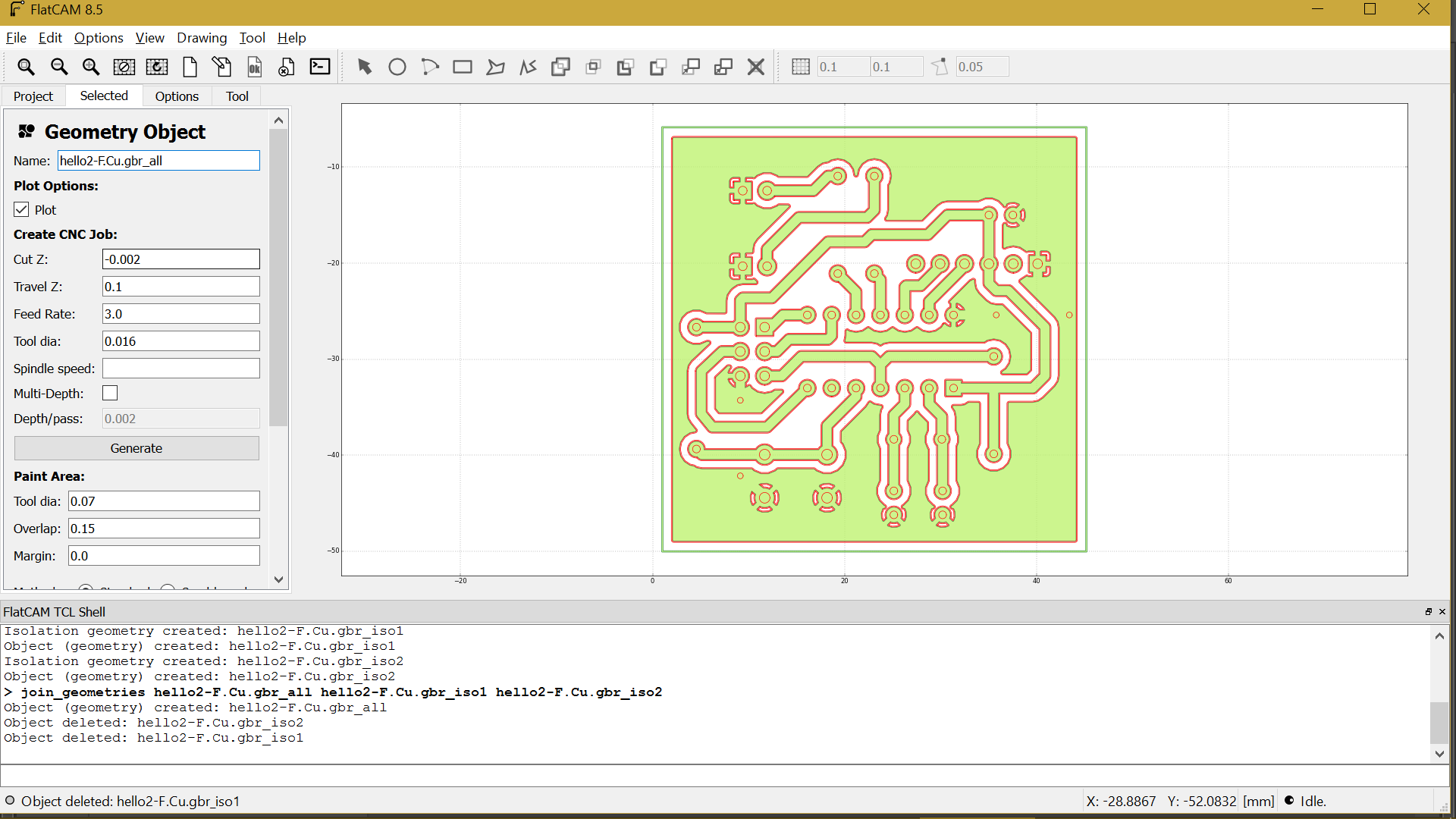
When you open the gerber file with the trace, you have to change to tool dia and the number of passes according to your CNC (here 0.1 and 2). When you click generate, I will create the path for the traces and two .iso files
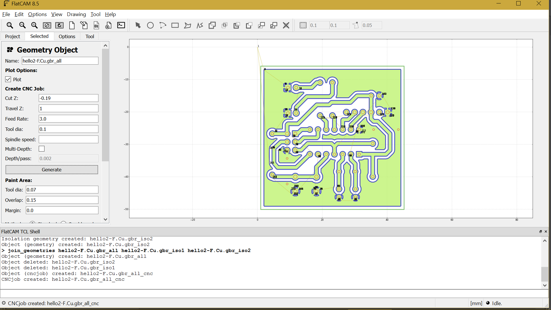
I have join in one file the two iso files via the following command : join_geometries hello2-F.Cu.gbr_all hello2-F.Cu.gbr_iso1 hello2-F.Cu.gbr_iso2. We are working in the "create CNC Job" tab with the following parameter : Cut Z : -0.19 (the depth of drilling), Travel Z : 1 (the distance the drill will go up and then move without milling), feed rate : 3 (cutting speed) and the tool diameter : 0.1. After clicking on Generate, I get the file needed for my CNC
The result seems correct so far
Now the drill holes file, almost same parameter, except I'm going further in the board with -1.7
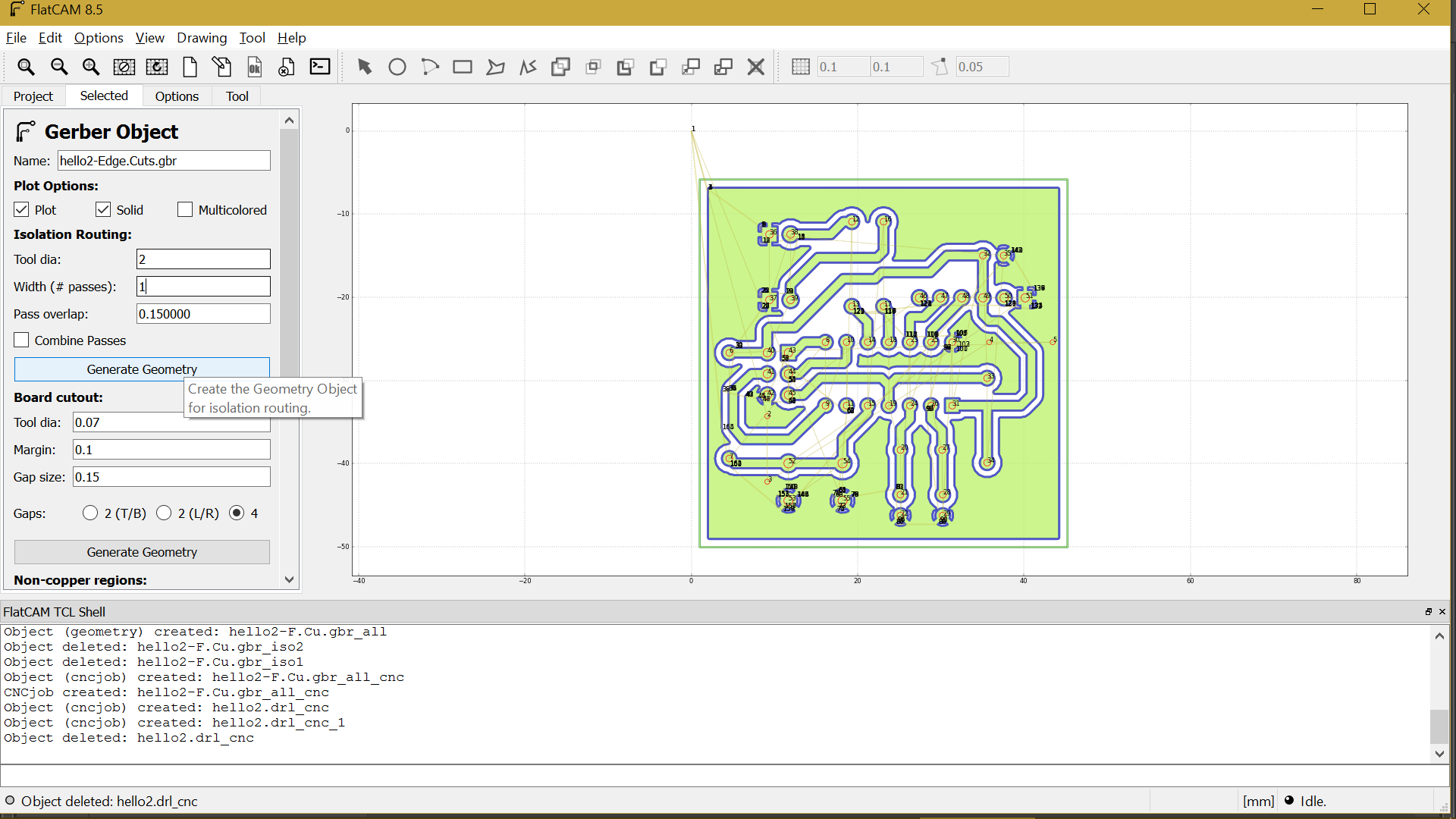
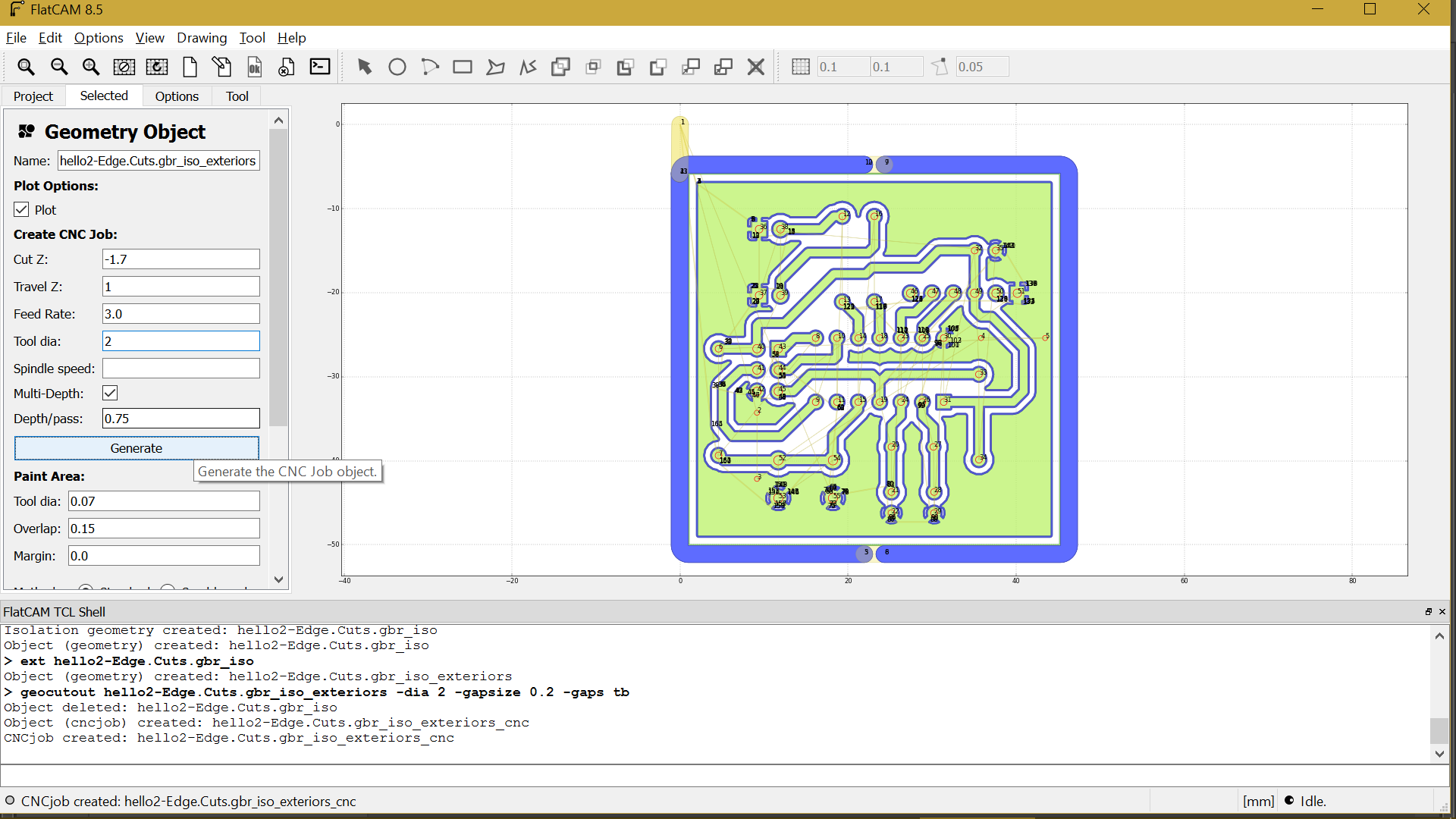
And the last one, the Edge Cut, I have indicated a diameter of 2 for my tools with only 1 passe.
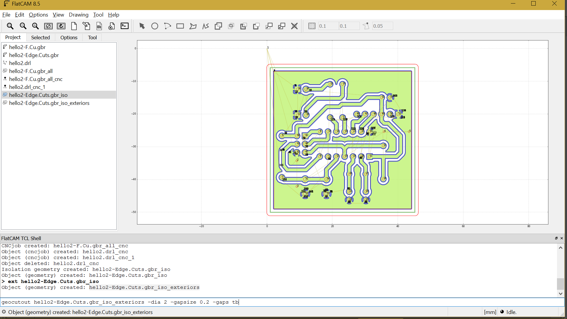
With this commmand, I have created the exterior cut of my board : "ext hello2-Edge.Cuts.gbr_isos"
I have also created two small bridges thanks to the following command : "geocutout hello2-Edge.Cuts.gbr_iso_exteriors -dia 2 -gapsize 0.2 -gaps tb"
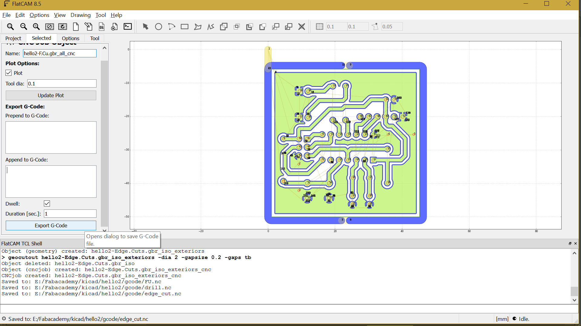
Now I have exported the 3 g-codes (one for drill holes, the Edge Cut and the Traces), CNC ime now
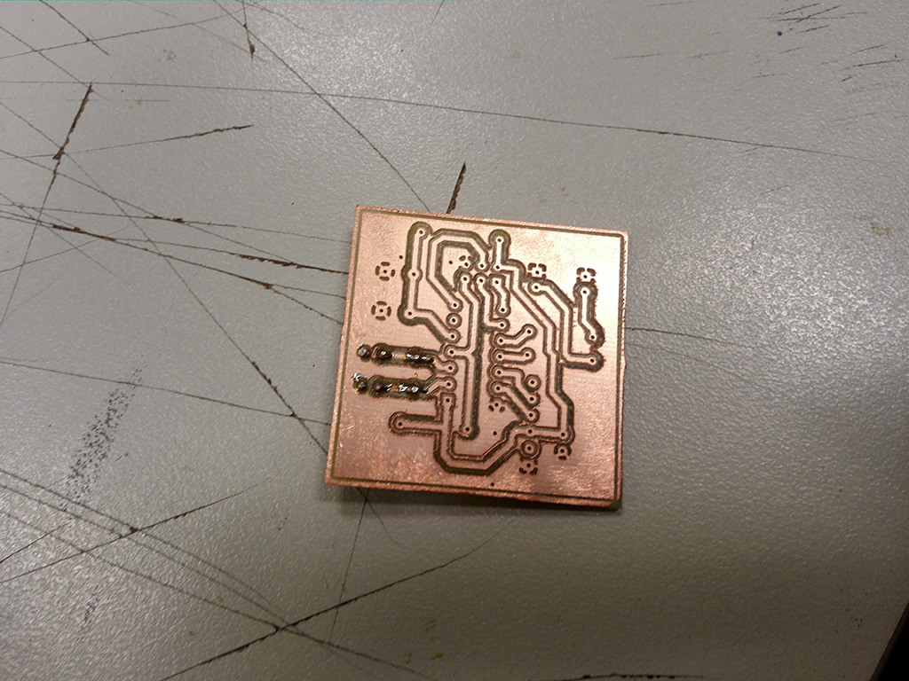
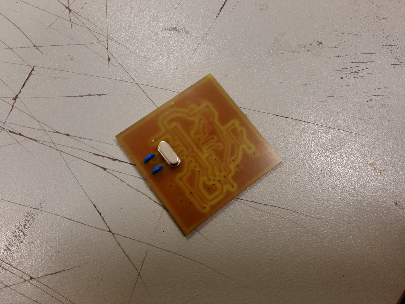
After some adjustements, I have milled the 3 files on my board and this is the result
And down
Finished
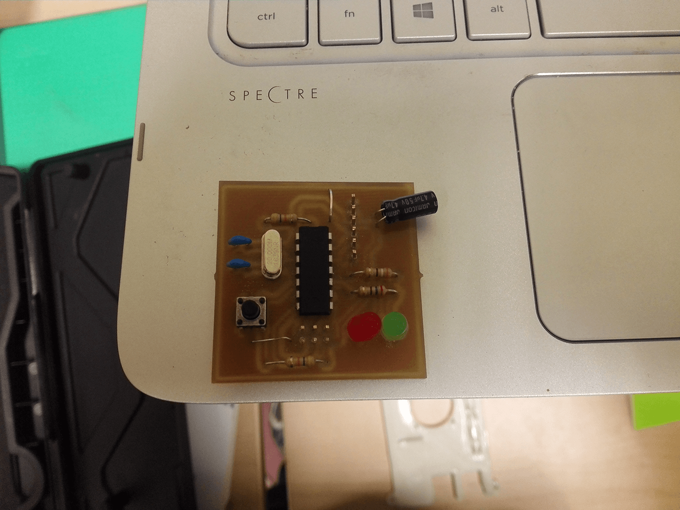
Summary : Electronic Design was a roller coaster between the design of the board until the soldering part My main difficulty was how to find how to connect all the components, first for the schematic and then on the PCB. I finaly succeed after a friend of mine explain how to look on datasheets or internet the correct pineouts for the connectors.
After that, It's a kind of trials and errors until you get the better combination (goind under the components such the ATtiny or the resistors is much easier !)
The milling was not too difficult and the soldering either. You just need to choose carefully the components you chose to begin with. I will quickly tried to make it blinked :)