Electronics design
Assignment
- Redraw the echo hello-world board.
- Add (at least) a button and LED (with current-limiting resistor).
- Check the design rules, make it (if you have time this week, test it).
- Optional: simulate its operation. Measure its operation
Learning outcomes
- Select and use software for circuit board design.
- Demonstrate workflows used in circuit board design.
Have you
- Shown your process using words/images/screenshots.
- Explained problems and how you fixed them, including how you worked with design rules for milling (DRC in EagleCad and KiCad).
- Included original design files (Eagle, KiCad, Inkscape, .cad - whatever).

Materials

Pin headers (3x2 and 1x4)

Designing and milling the board
-
Because our milling machine has still not arrived to the lab, we had to design and send the files to Ima6ine for the milling job. Also, by advise of César we decided not to design and mill the echo hello world board, but another one based on ATtiny45 that we could program to control other circuits.
We used Eagle software for this excercise, I later repeated the entire process using kiCAD, as I'm trying to use as many open source tools as possible.
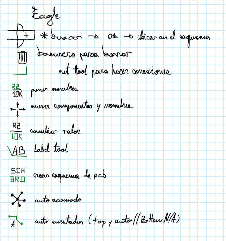
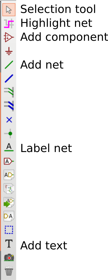
This is the list of eagle commands that I used throughout the process:
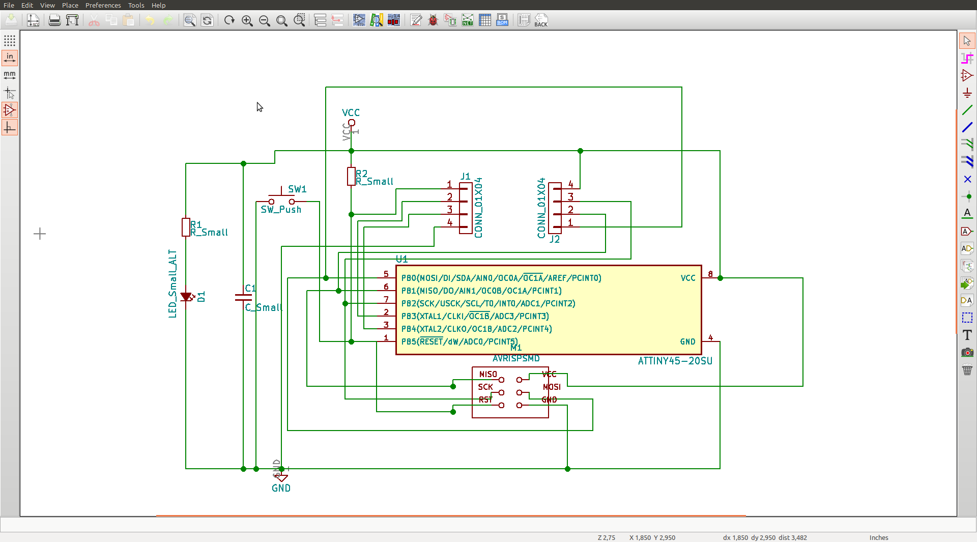
We started drawing the schematic for the board, first the microcontroller, then other components and the pin headers for programming and connecting to a circuit. When we finishe the schematic, we added a button and an led to the board. Since we will need the free pins to use as input or outputs for later circuits, we decided to add the led as a power indicator, and the button as a reset switch. This is the schematic we drew:
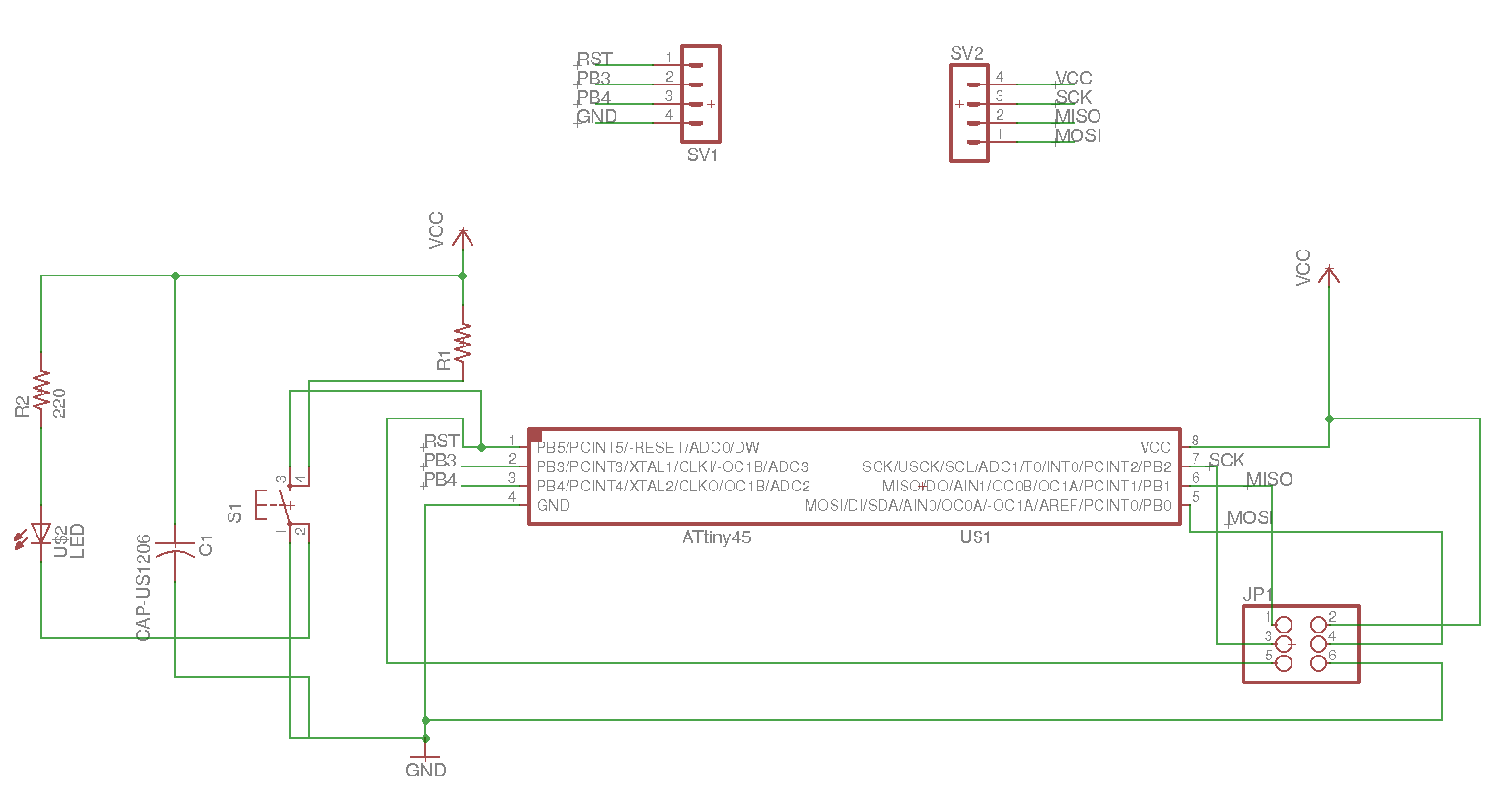
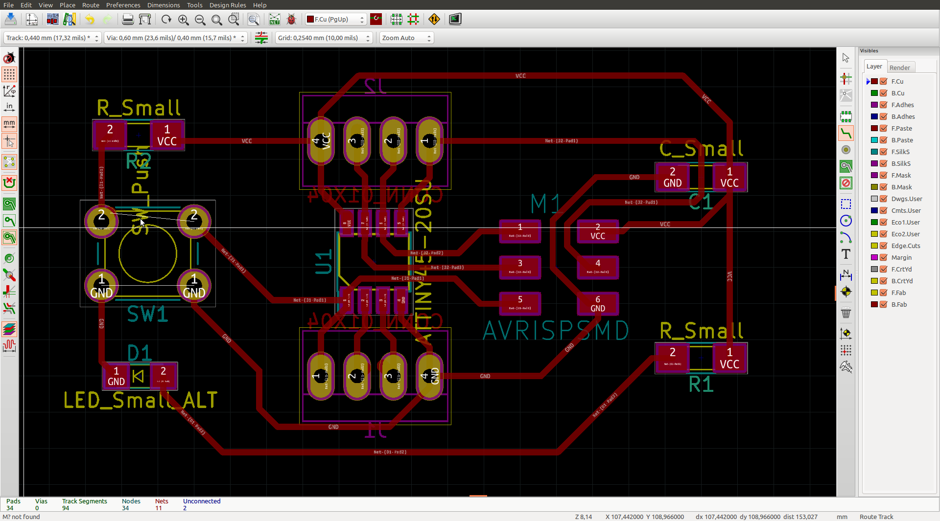
On the schematic I used net tool to make the connections for all components except for the 1x4 pin headers, for wich I used route names. This allows a little more flexibility when editing the routes on the board.
On the board I arranged the components simetrically around the microcontroller and then drew the routes manually. Because the button has four terminals connected internally in pairs, I used it also as a bridge, so a route could be traced below it (it can be seen between the pads of S1).
The routes were traced avoiding 90 degrees angles, and where given some space around.
-
Then I repeated the process with kiCAD, I is the tool I will be using more often for my assignments.
In kiCAD. The schematics, pcb, footprint and other tools work each one on their own.
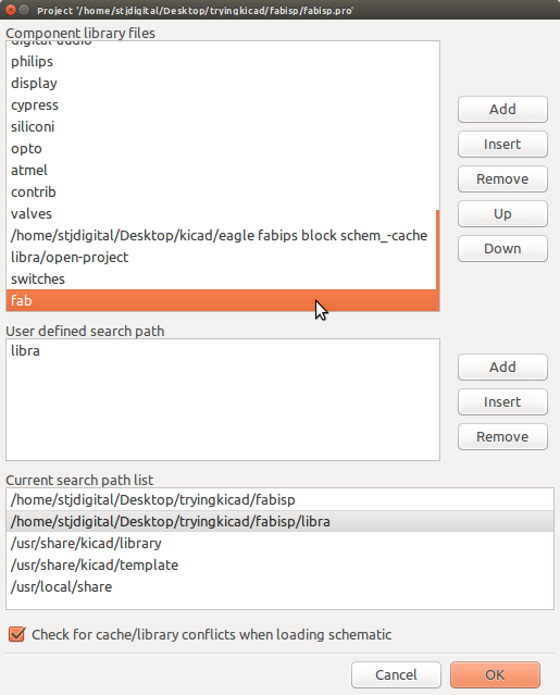
First, for the the schematics, I imported the fab kiCAD library:
Then, to create the schematics, these are the tools I used:
This is the schematic:
After this, there are several steps needed before the pcb design:
- Rules checK
- Associate footprints to components
- Generate net list
-
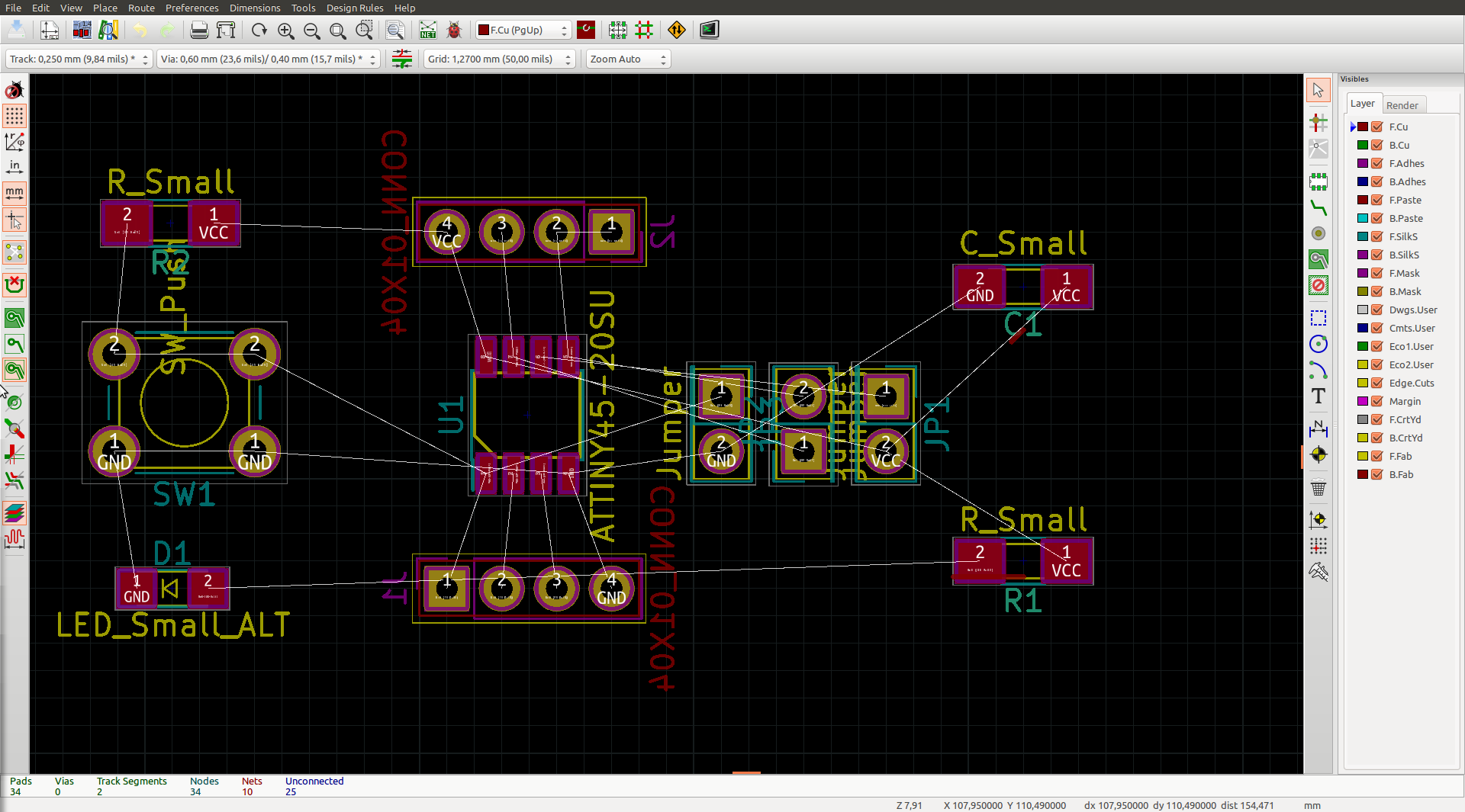
The pcb design let you place the componets on a pcb, and create the nets to connect them, wich will be milled by the machine.
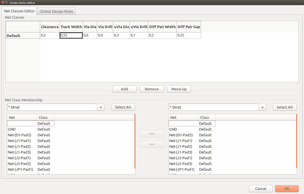
First, I defined the net width. We found that a value that works well for the pcbs is 0,55. Thinner nets are too freagile. The clearance was left as 0,2, the nets were not too closer with this value, but I do not know whether this parameter is kept through the gerber creation process.
Then, the components were distributed and the nets were placed. I changed some footprints for a better distribution of nets.
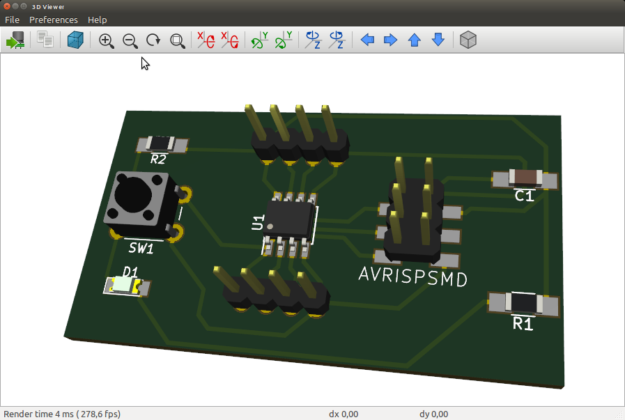
KiCAD lets you see a 3D model of your pcb<
-
Modifications to the board
The button was added between reset and GND. So when the button is pressed, the reset pin (wich is normally high) is connected to GND, and the board is reset.
The LED with its current-limiting resistor in series was connected between VCC and GND, so when the board is powered, the LED is on.
The current-limiting resistor was calculated to be 500 Ohm (V = 5V, Imax = 10mA: V/I = 500 Ohm).
Finally the board was exported to png format and sent to the milling machine.

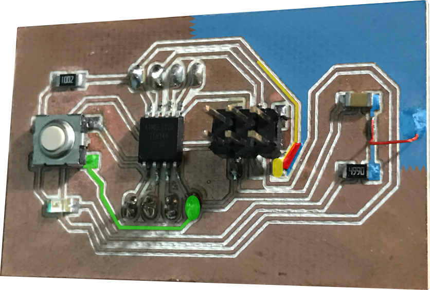
Soldering the board and solving problems
-
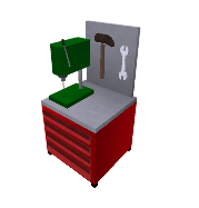
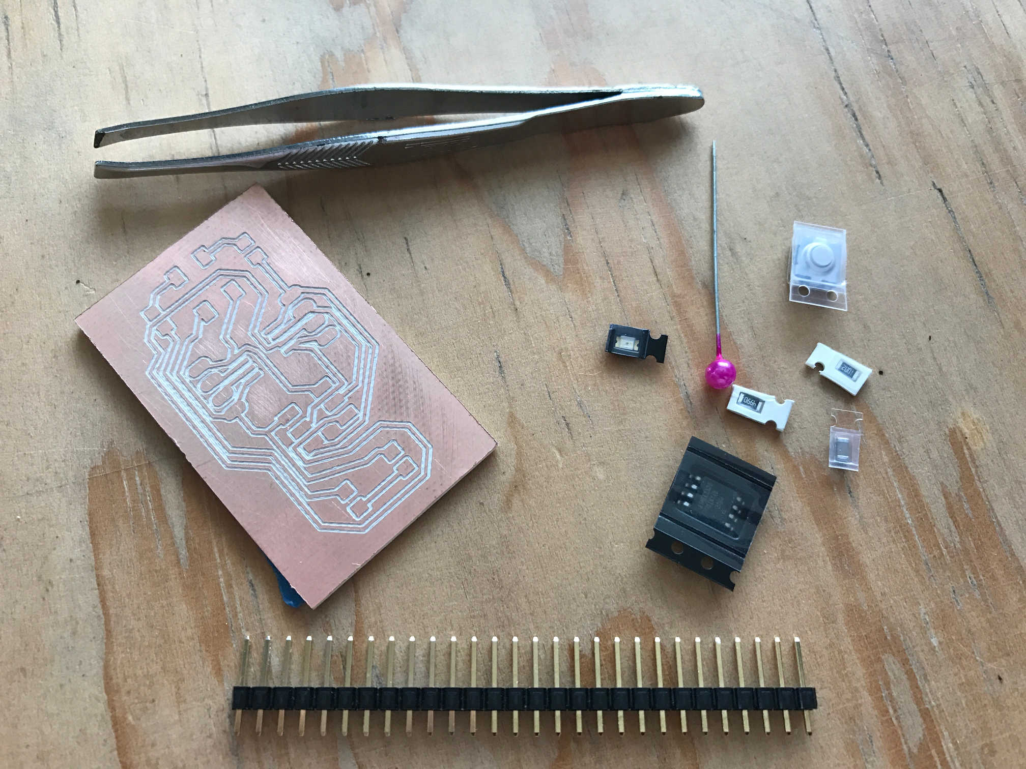
These are the components for our board:
And this is the process of soldering the board:
Mistakes and solutions along the process:
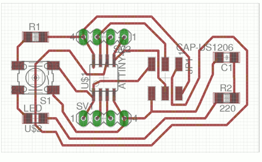
- Before sending the file to the milling machine César Cruz helped me find a missing ground for the LED, so it was solved in the schematic (green route in the picture).
- When soldering the board, I found that a VCC line was missing between C1 and R2. It was solved with wire bridges. The yellow VCC line was connected to the blue area in the picture, and from that area to the node between C1 and R2 with the red wire bridge to the right of the picture.
Back