Week 6: Electronics Design
Assignment:
- Redraw the echo hello-world board , add (at least) a button and LED (with current-limiting resistor), check the design rules, and make it
This week my assignment is to redraw the hello-world board ,and add a switch and LED and finally mill the PCB in milling machine and solder it manually.
printed circuit board
A printed circuit board (PCB) mechanically supports and electrically connects electronic components using conductive tracks, pads and other features etched from copper sheets laminated onto a non-conductive substrate. Components (e.g. capacitors, resistors or active devices) are generally soldered on the PCB.

The PCB used in our lab is FR1 machinable blanks.These circuit board blanks are made by bonding a thin layer of 1 ounce of copper over one or both sides of the entire substrate. To etch a circuit design into the material, unwanted copper can be removed using a CNC machine, leaving only traces. Free software like Eagle CAD, a vector based 2D program like Inkscape or a 2D raster program like gimp will work for designing circuit patterns to upload to the machine for milling. The circuit can also be drawn on the boards using a chemical mask pen and then chemically etched to remove the unwanted material.The more commonly available FR-4 boards have a fiber glass, non-conductive layer which wears the bits on the machine very fast and will produce undesirable fiber glass dust during machining. These FR-1 boards are made with a cellulose paper-based material which makes the dust less toxic and the resin binder is soft enough that the bits last much longer.
PCB designing
Printed circuit boards, PCBs, form an essential part of any electronics equipment these days. The PCB design and layout forms an integral part of the design of the whole product, and it can be the key to the success of the product meeting its performance requirements in many instances. PCB technology has progressed significantly in recent years. The design technology has improved with PCB CAD systems and PCB software to layout the boards better, and also analyse the performance under conditions such as the operation at high frequencies. In addition to this the technology for the manufacture of PCBs has improved enabling far smaller tracks to be used as well as incorporating features such as multilayer boards with blind vias, etc..
The steps involved in PCB designing are
1.Parts research and selection
2.Schematic capture and simulation
3.Board Layout
4.Fabrication
PCB designing software
Printed Circuit Board (PCB) layouts are designed with help of PCB drawing software’s, commonly known as pcb layout design software. PCB design tools fall into many categories based on their development platform, pricing strategies etc.Some of the Open Source PCB Design Software are listed below
1.Eagle
2.123D Circuits
3.KiCad EDA
4.Altium
5.Proteus
Eagle
Eagle is one of the most popular Circuit drawing and PCB layout software available in the market. Most professionals,students and hobbyists find Eagle as an ideal choice for their PCB development needs. Eagle in fact is an enterprise PCB designing software but they are offering a lighter version (with limitations compared to enterprise application) for free download. And Eagle will run on Windows, Linux and Mac.
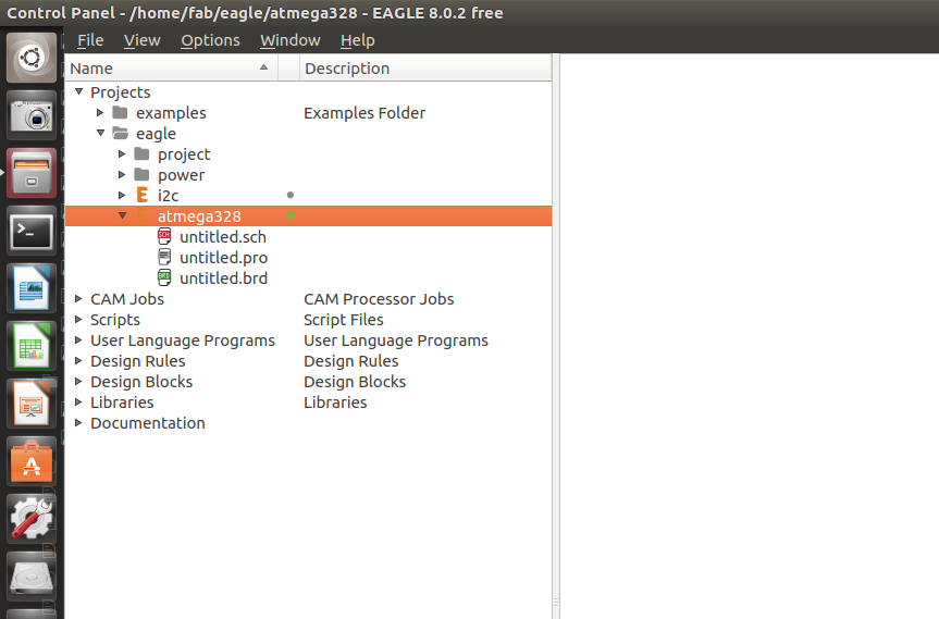
In order to make the process of designing easier we have been provided with default fab library fab.lbr , which I downloaded and added to the library in Eagle. which was then used for drawing the schematic
The fab.lbr will not be available even if we have put the file in the library folder,inorder for adding components from fab library first of all ensure that the green button of the fab.lbr has be activated by opening library from the Eagle main window.
I started with Eagle for drawing the schematic of the hello-world board given below

A breif idea about electronics canbe obtained here.
Procedure involved in drawing schematics in Eagle
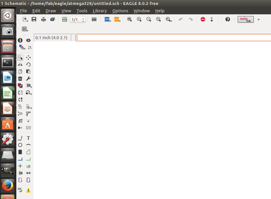
open the eagle ,the below screen will be comming.
Click file and open new schematic.A new window appear the screenshot of the window is given below.
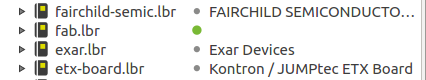
Since we are doing FAB ACADEMY,the components used should be all from the fab lab itself.There is a seperate library for fab components,in order to access the fab components, First of all click libraries which is shown in the first screenshot .A list of libraries will be comming.From there select the fab and activate the button .when activated button become green.
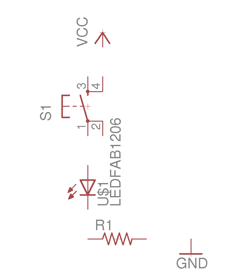
Now we can start designing a small circuit,which is used to turn on the led when the switch is pressed.It is just an example to show how to draw the schematic. In order to add the components press add and the below screen will be comming .
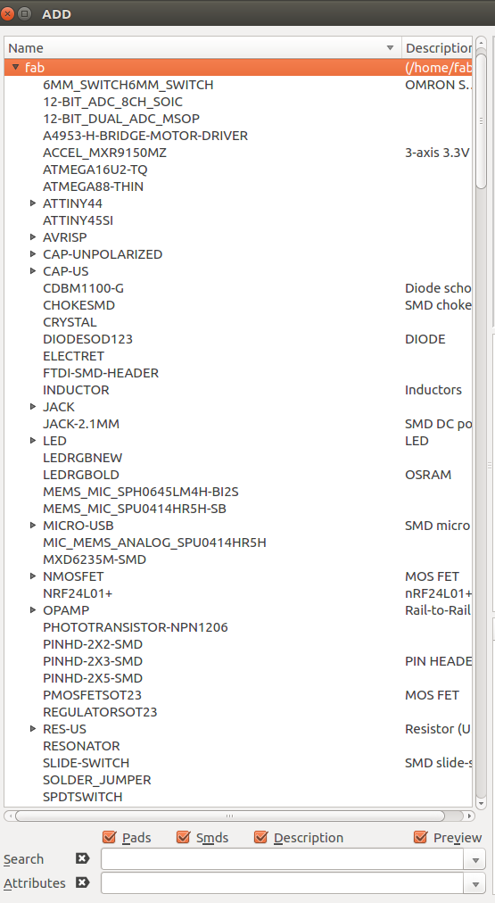
Now select a switch from the fab library and the process is well explained in the below figure.
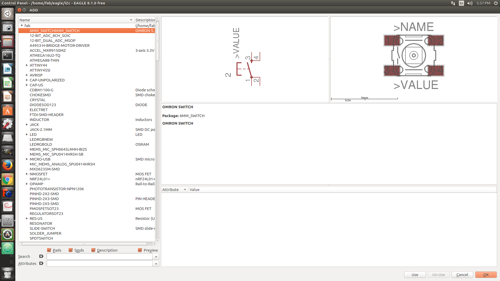
After selecting the component ,click ok to navigate to the window of schematic where we have to place the component.Now for selecting other components press Esc.
In the similar way select all other required components.Finally we will get all the components required for our Schematic.
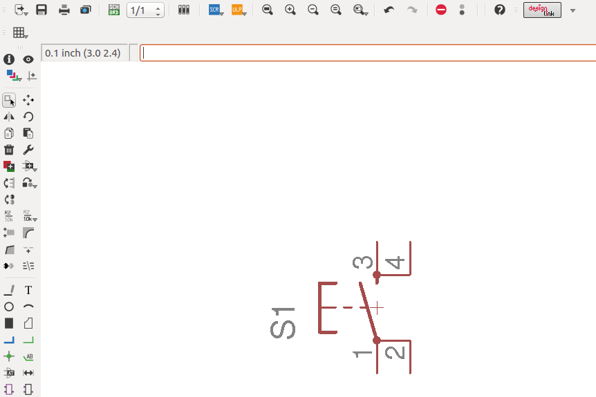
now we have to connect all the components.We can use a command "wire" for doing so.
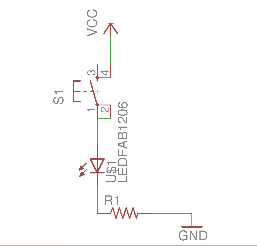
now using the mouse connect all the components .The connected schematic is shown below.
now it is time to go for board design,click the Generate/switch to board and we will be getting the below screen.
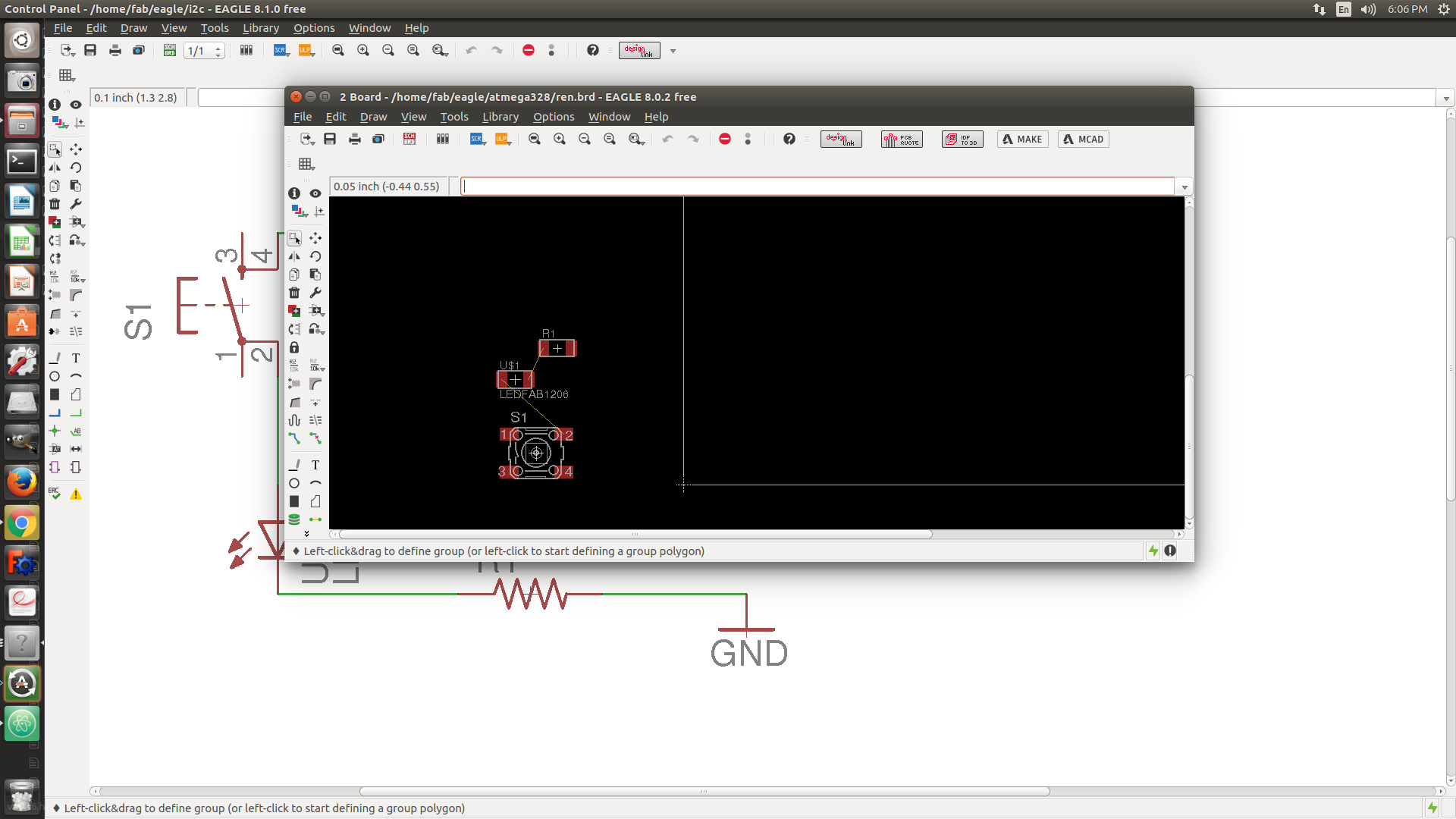
again using "move" command place all the components to the location where we want to place the component in our PCB.
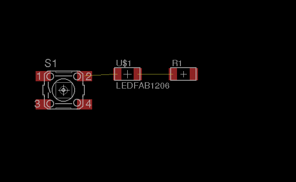
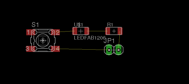
now there is no pin out for my circuit so I have to switch to schematic and place the pin,which has to be again added .

now the schematic is ready,so we have to go to the board and move the component ie the pin to the correct location.
Now in the board we have go for routing.The procedure should also include the design rule which is defined in the next section.
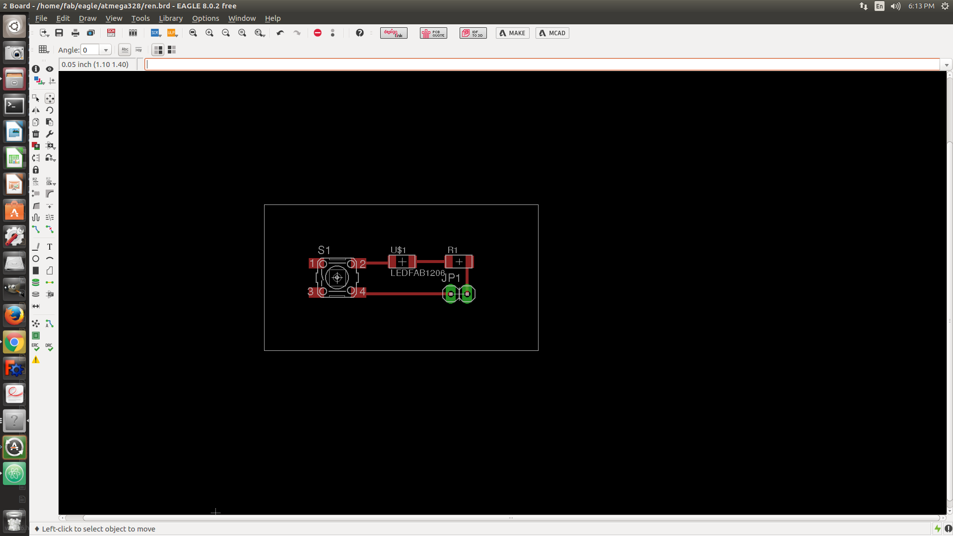
now we have to set the dimensions for our pcb and the above figure show the board dimensions reduced in such a way that no space is wasted.
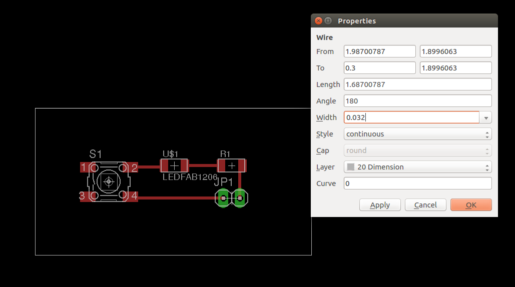
Each of the boundary lines has to be given a thickness of 0.032 inch in order to properly being cut out from the modella.
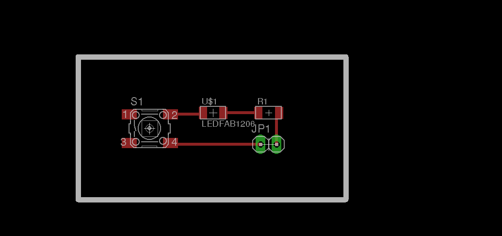
finally my example board is ready ,so using layer selection we can export the mill trace and cut trace for our board.
the above process has to be replicated for designing the Attiny44 board,using the fab library.
Attiny44 board designing
The schematics drawn for milling in Eagle is given below

The components used in the process are
1. ATtiny44-SSU: datasheet
2. 20mhz resonator: ATtiny has an inbuilt 8mhz clock, but this one is faster and more accurate
3. 6mm Switch Omrom
4. AVR ISP SMD header: for programming the board
5. FTDI SMD header: powers the board and allows it to speak to the computer
6. 10K resistor(1)
7. 499 ohm resistor(1)
8. 1µF capacitor
9. LED
The resistor in series with LED is calculated using the Voltage -Forward (Vf) of 1.8V and DC Forward Current of 20mA (Ifc) obtained
from datasheet To calculate the required resistance:
R = (Vs - Vf) / Ifc = (5V - 1.8V) / 0.02A = 160 Ohms
I used 499 ohm
Layout
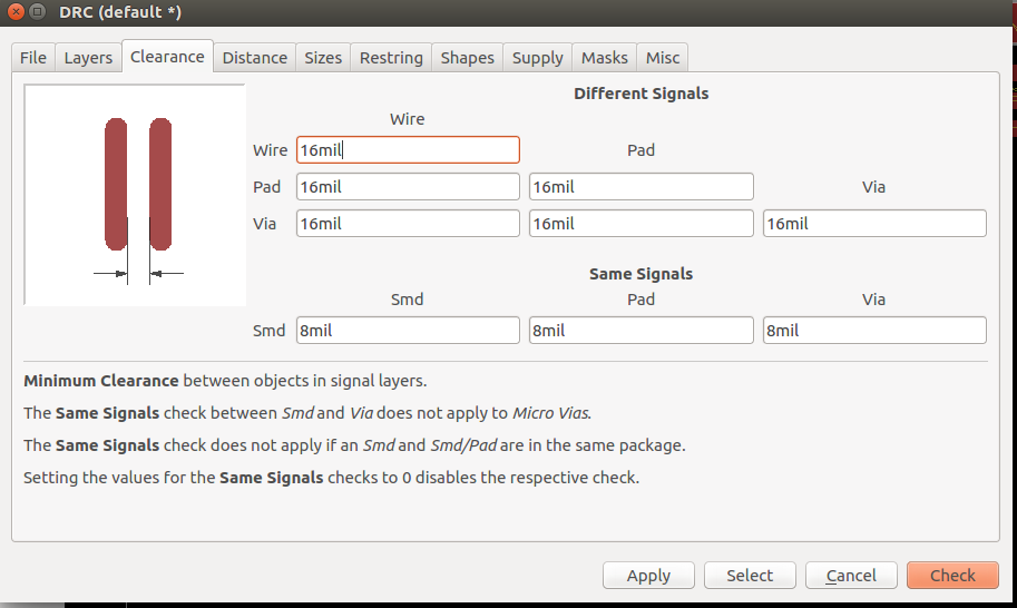
After the schematics is obtained we have to Generate/switch to board for getting the Board Editer ,where we have to set the design rules and route our circuit.
|
|
|---|
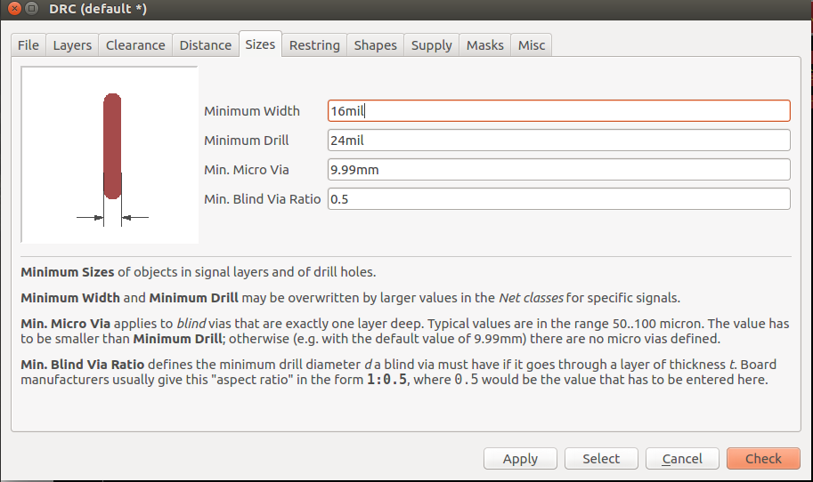
The Clearance tab defines the various minimum clearance values between objects in signal layers.
The Sizes tab defines the minimum width of any objects in signal layers and the minimum drill diameter.
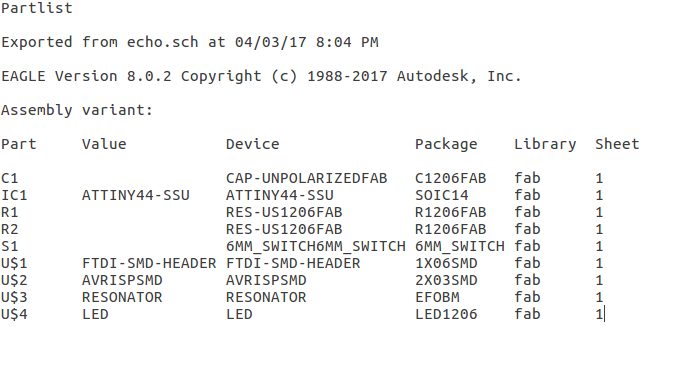
Part list verification is done carefully.The netlist which gives the connection details and the parts used in the circuit design are given below.

|
|
|---|
By comparing the netlist and the schematic the connections are checked.

The final layout of Echo hello World which I obtained is given below.

Export the layout as a monochrome png at 1500 dpi. Here is the mill trace:

Here is the cut trace which is obtained by exporting from the layout followed by value invert in the GIMP .

Milling
I used Fabmodules offline webmodule version for connecting with the PCB milling machine.The process is explained below

open another terminal window


type "localhost:8000" in the browser.After that wehave to import the mill trace png and do the settings.Milling with Roland Modella MDX-20 should be done carefully ,first of all view mode is selected and the drill bit of size 0.4mm is put into the tool post and after that move to (xmin,ymin) which should be calculated trial and error with out damaging the bit

after the minimum position is obtained,push the bit down ward sothat it reaches the pcb and just drill it.after that press send.The process will start.

The same procedure is used here,the bit shouldbe changed to 0.8mm because it should be cut.

My completed board is here

I tested my board with the C code and make files for Attiny 44 is downloaded from here .The two downloaded files hello.ftdi.44.echo.c and hello.ftdi.44.echo.c.make are placed in the empty folder.

open terminal in the curent folder and type the command:make -f hello.ftdi.44.echo.c.make

connect the usbtiny module to the computer and connect the board to the usbtiny using ISP cable and check the connection by typing the command:lsusb

open terminal in the curent folder and type the command:make -f hello.ftdi.44.echo.c.make program-usbtiny-fuses

open terminal in the curent folder and type the command:make -f hello.ftdi.44.echo.c.make program-usbtiny

now connect the FTDI cable to the system and conect the board to the FTDI cable .type the command:sudo cutecom ,the cutecom window appears,click open device and type the message to be communicated with the board which will be comming back

finally I have checked my board ,it is working fine
Download my design file from here