NOTE: Vigyan Ashram is known as "Fablab 0" , it is one of the remotest labs with very minimal internet access , therefore, we have been using old version of Fab module which is an offline version.
WEEK 6
Electronics Design
Neil's Appreciation for Hello board on 17/05/2017 @1 hour-3 minutes and 58 seconds
WEEK ASSIGNMENT: Hello World Board
USING : Eagle, Photoshop and Rolland Modella
Learning Outcomes:
1. Redraw the echo hello-world board with Eagle
The proper workflow in designing a circuit is as follows:
-Design the schematic.(ERC (Electrical Rule Check), Choosing the right component package)
-Board Layout (Optimal component placement for minimal signal path,Routing)
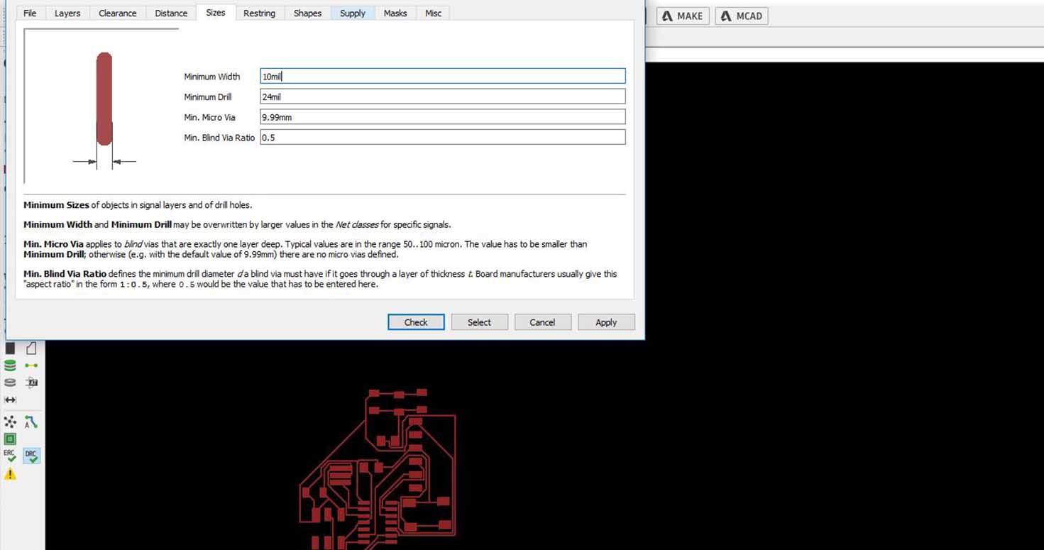
-DRC (Design Rule Check)
-Milling
-Stuffing
-Debugging
Firstly, going through resources given by fab academy about the components, methods and softwares.
Then we had a brief inroduction given by our instructor about the week's assignment.
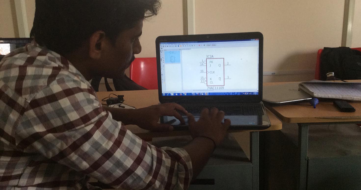
Using Eagle which i had installed before
I followed the following steps:
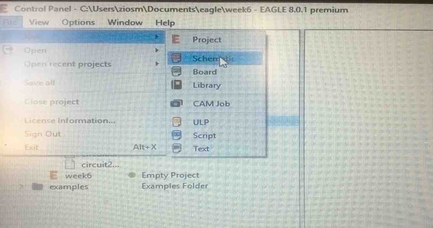
1. Open Eagle and login if you using first time.
2. Make a new project
3. Choose Schematic
4. Select Option USE to choose library.
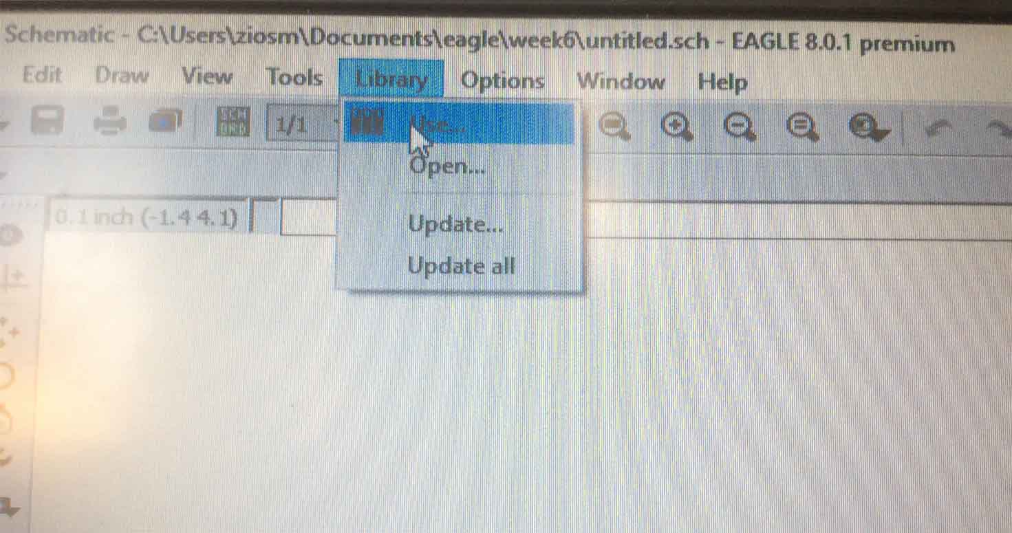
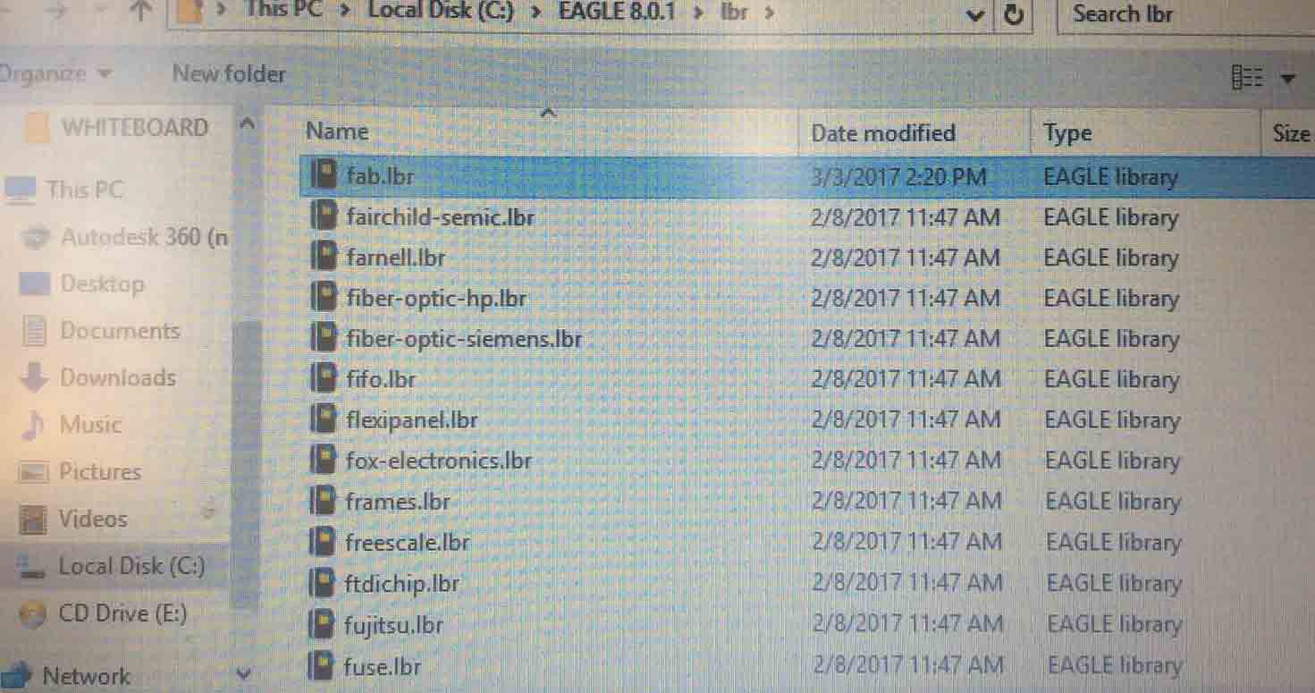
You can download fab library from this
Fab.lbr and other libraries can be downloaded by going to Manage Libraries in Options.
5. Switch the Grid ON , i changed value to Size : 0.01 and Alt : 0.025.
6. Write Command ADD to add components.
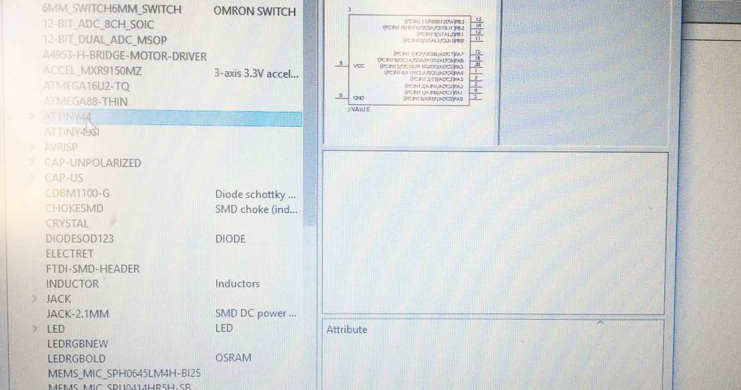
7. You will see the fab library there, you can start adding components.
8. I started by adding ATtiny 44, placed it on the board, Press esc and choose next.
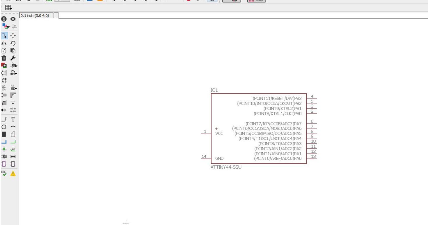
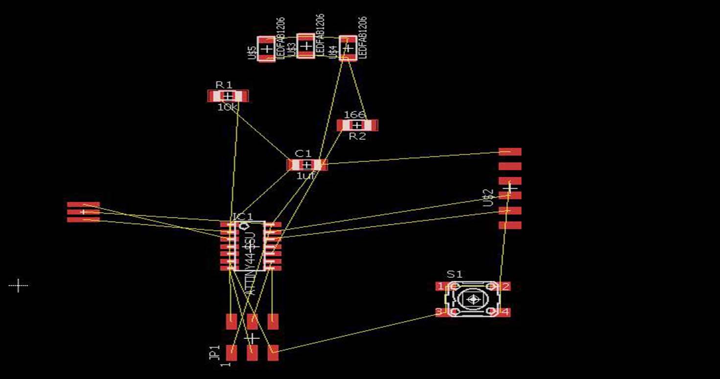
9. I placed all components on the board with reference to this hello board.
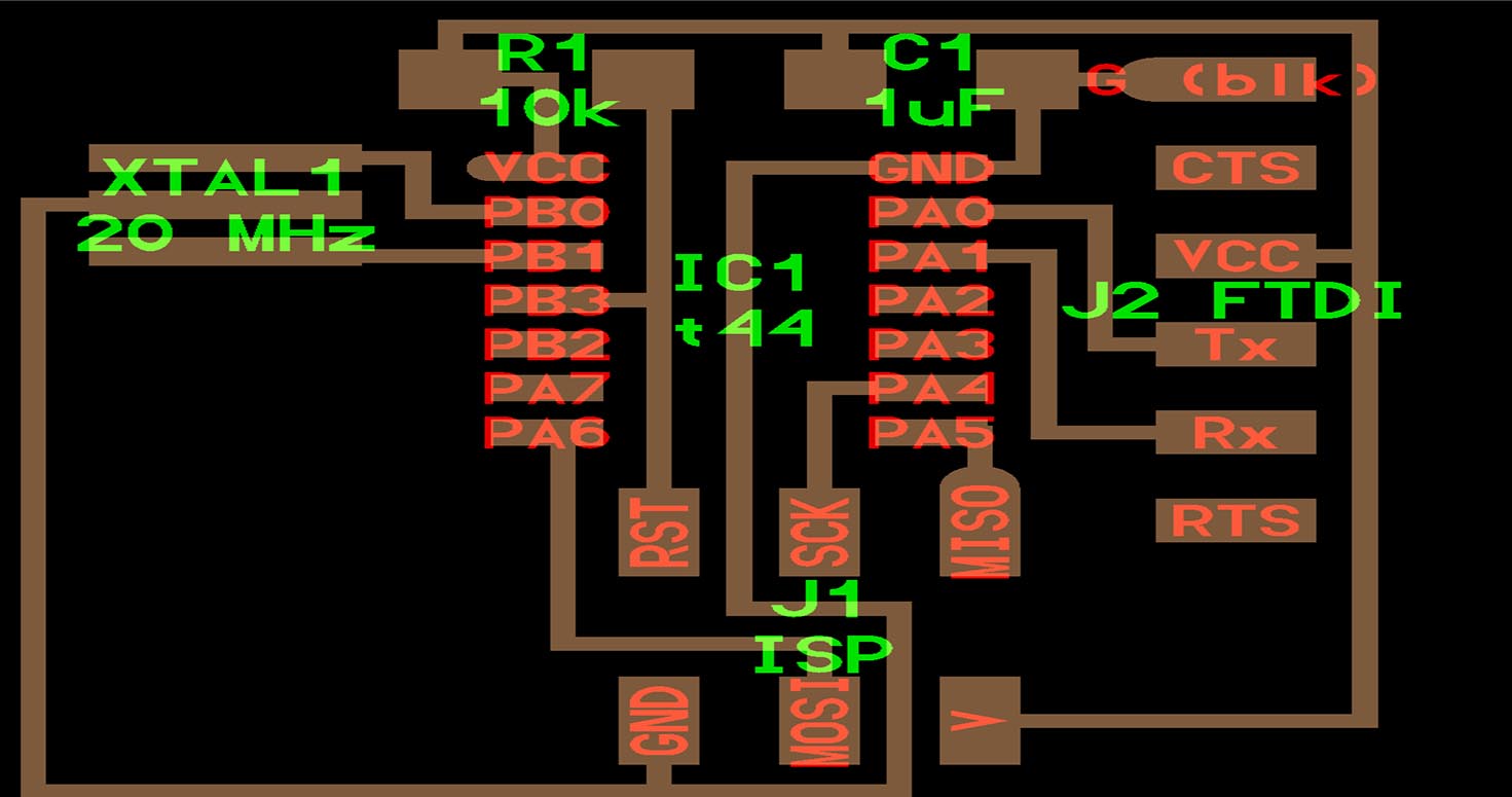
10. Started making connection by using command LINE.
11. Connecting points with JUNCTION where there are joints which you want to connect, not the joints which are intersected but connected. Its a good tool for joints.
12. Check errors by choosing ERC in tools. Recheck all errors as well as warnings. I ignored warnings the first time so i had to redo my whole schematic.
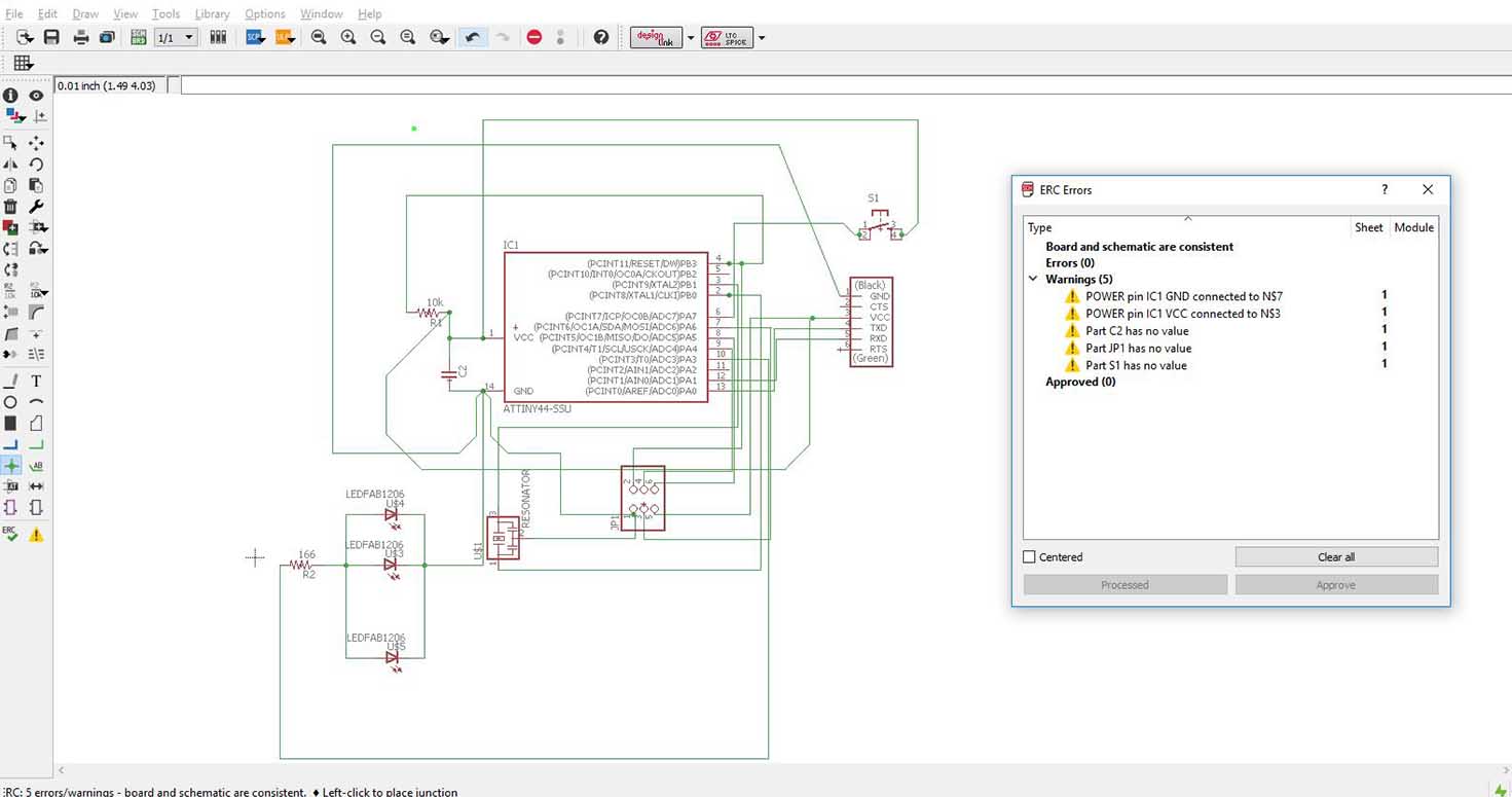
After switching to board the first time, i realised my resistor is still not connected to capacitor and capacitor is connected to wrong VCC, well i was loosing my patience because of so much chaos on my board.
So, i decided to move back to my schematic board and start connecting wires once again, this time i did ERC in schematic and DRC check in board.
The following Components were used for this board:
a) Resistors
b) Capicitors - 1 uf
c) IC Attiny 44
d) Connectors 2x3 and 6x1
e) Resonator
f) LEDs
(Added 3 LEDs in Parallel series)
g) Switch
13. Switch to board.
I did DRC to check design rules and change the size of the wire according to the diameter of the mill bit.
Then i was in dilemma if i should opt for Manual routing or auto routing. I wanted to manual route it but then i wanted to save on time. SO i went ahead doing auto routing.
I did Auto routing , got one 100 % variant, selected that.
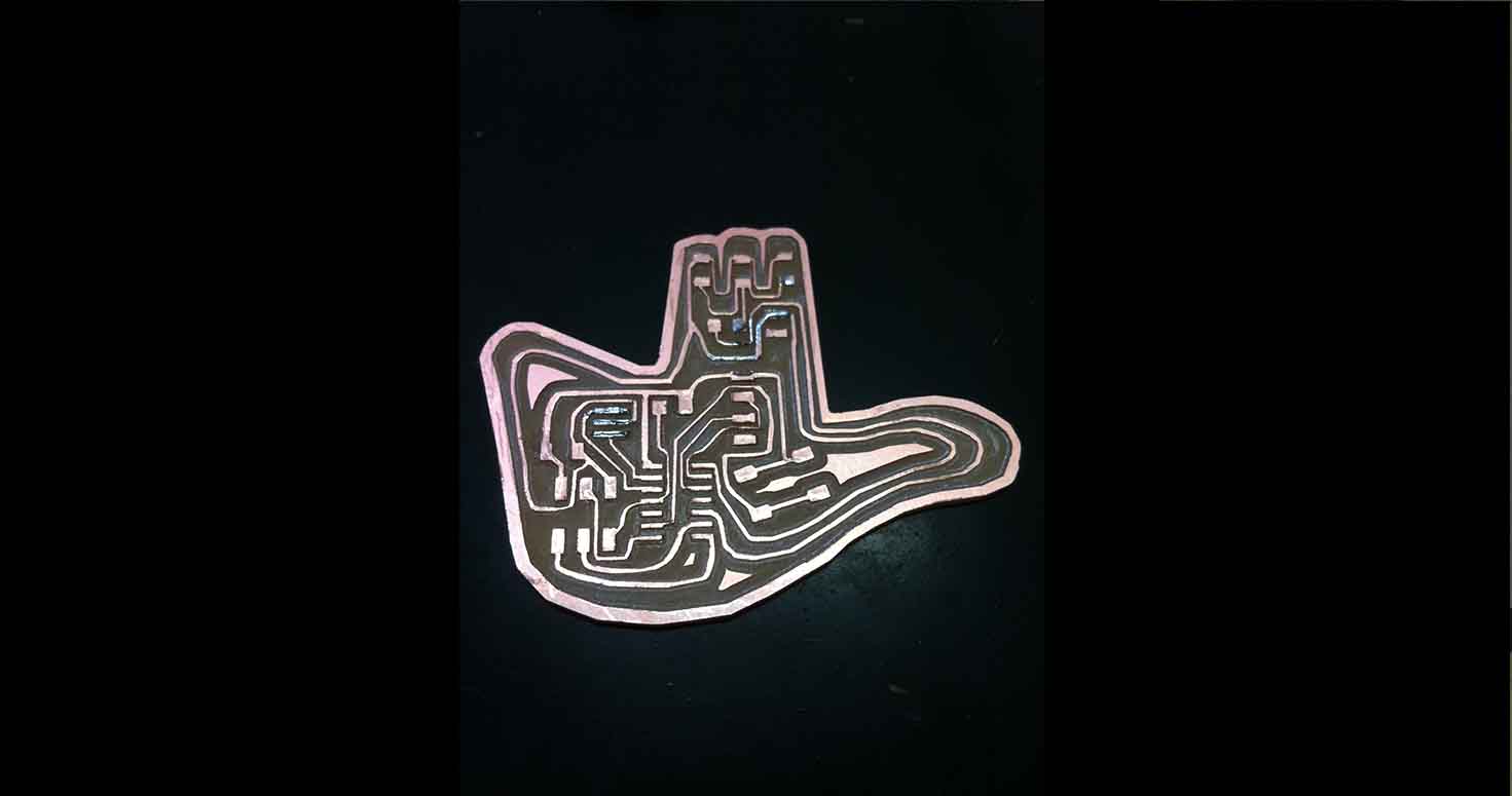
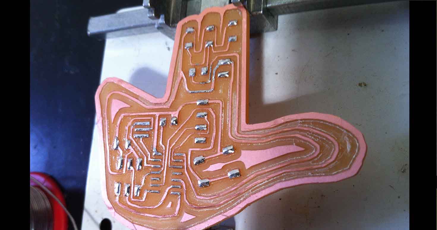
Now i planned to design my circuit in the form of an OPEN HAND, It is the emblem or symbol of the Government of Chandigarh and symbolizes "the hand to give and the hand to take; peace and prosperity, and the unity of mankind" Chandigarh (my home city, i have been missing since few days), Its india's only planned city designed by the great french architect Le Corbusier and known for its greenry.
So i first chose image of open hand from internet, opened in photoshop, edited and saved it in bmp in monochrome.
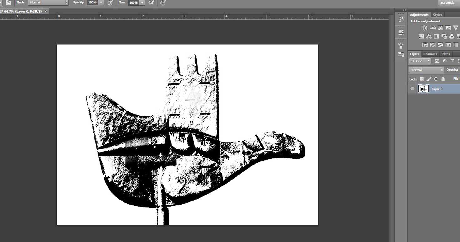
I used Topoz feature to edit image to sketchy look.
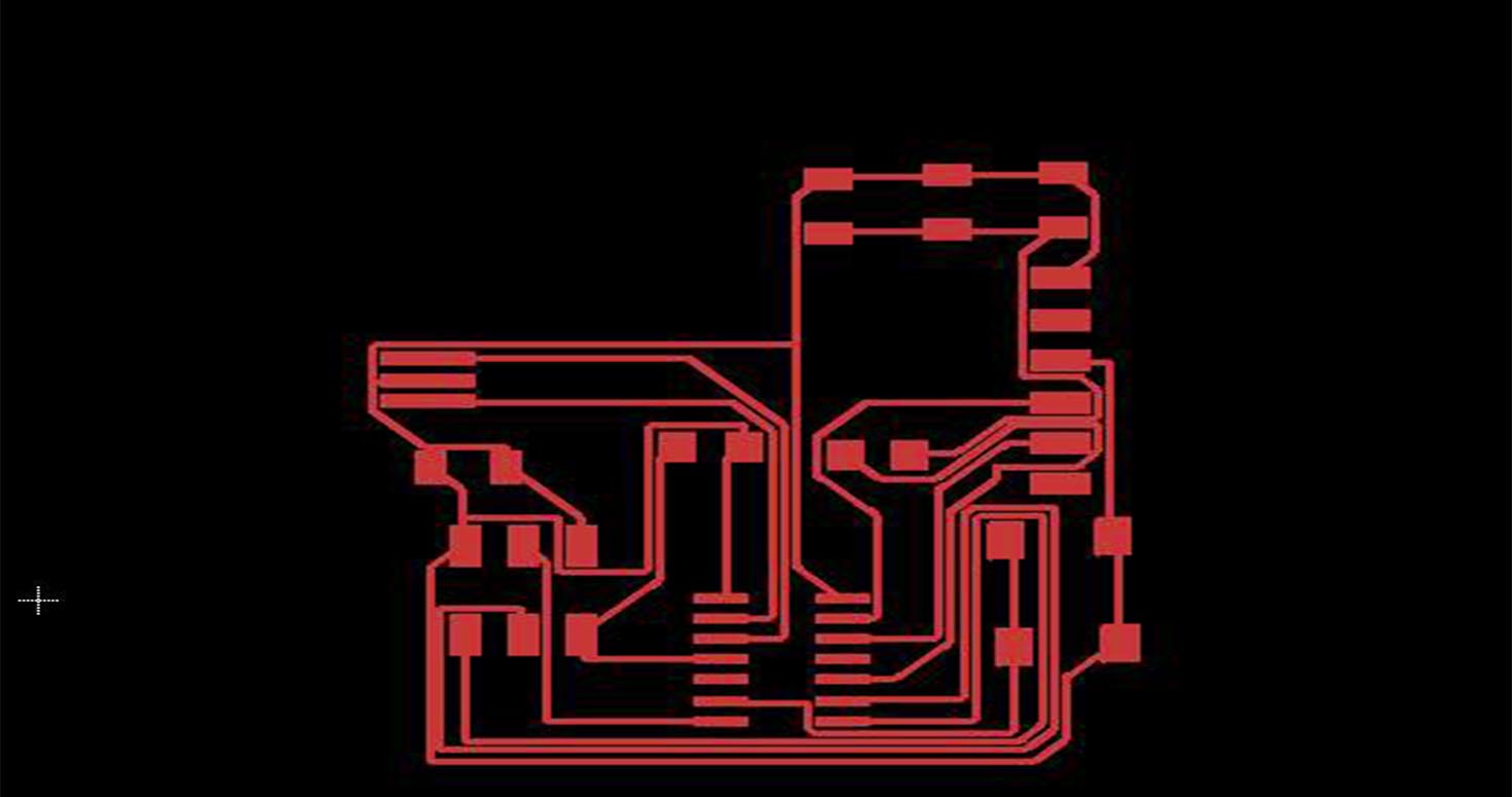
I imported BMP to eagle, picked compenents and overlayed over my picture to fit and again auto routed, this time i got 3 times 100 %, so i chose one, positioned them bit more to bring them closer enough to fit.
And then i unselected all layers except pads.
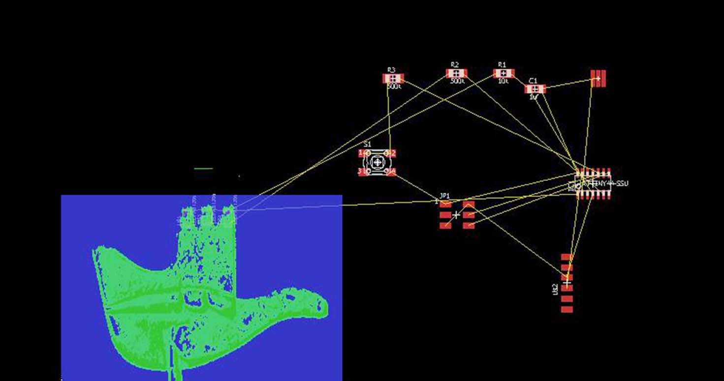
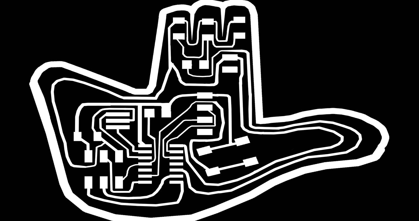
Saved it in png monochrome format with 1000 resolution.
Open this circuit over my open hand in photoshop, made adjustments, manipulations and increased the thickness of the lines, check distance between them , calculate milling bit diameter etc according to few design rules we discovered in a discussion with our instructor.
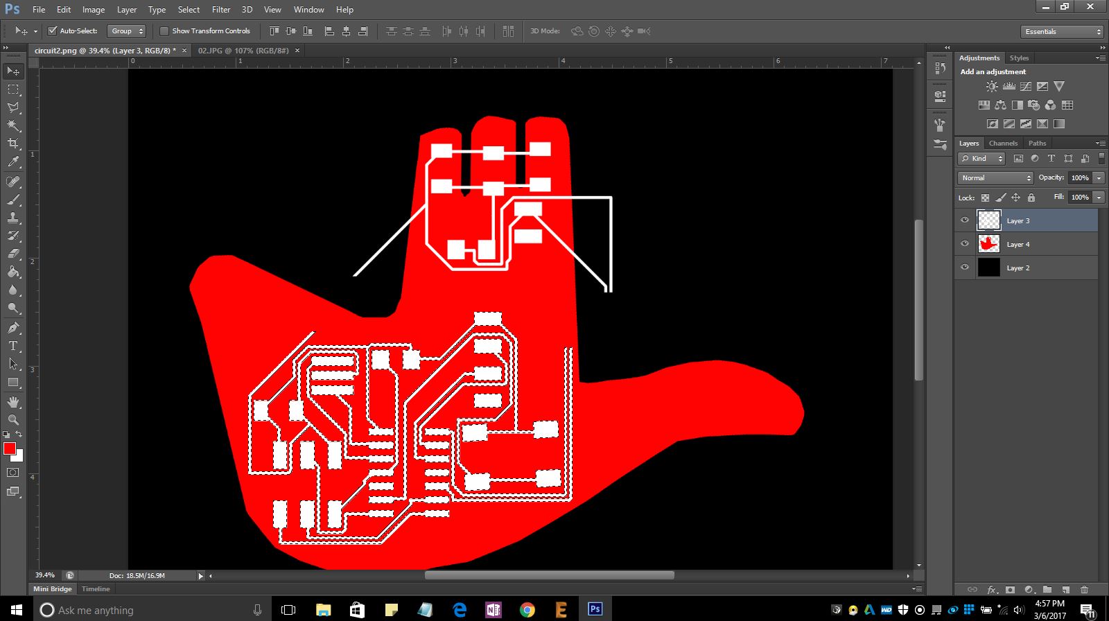
Had to move my compenents without altering their pad size, but wanted to give enough space among them beccause there was higher chances it will get short if kept so close which i didnt realise while making in eagle.
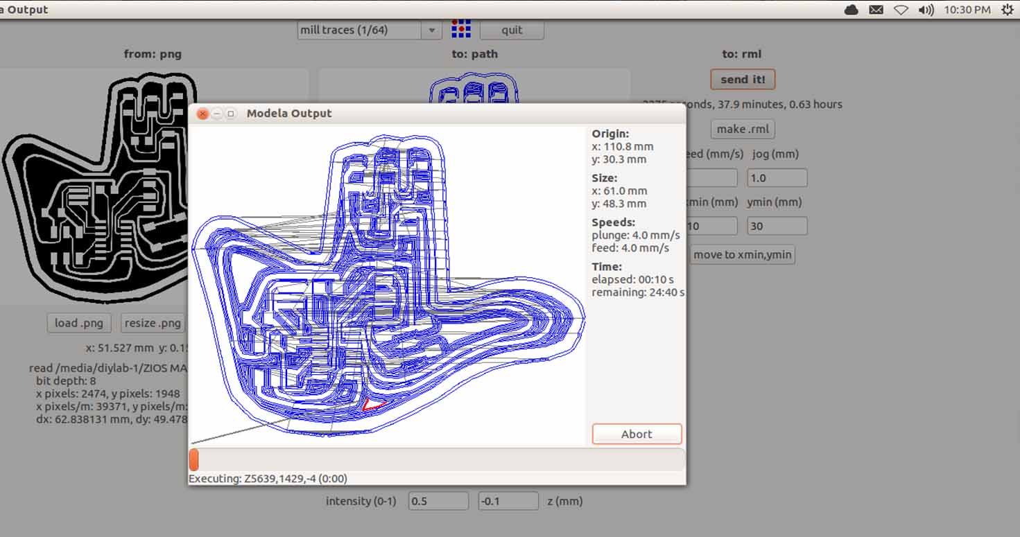
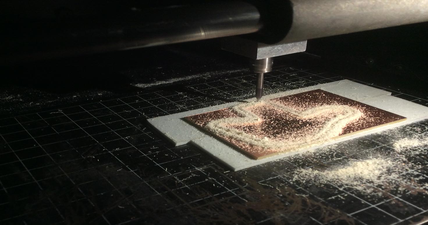
2. Making the PCB
I have used 1/32 to cut and 0.010 mill bit to trace my final PCB.
I used two types of mill bits , firstly for traces, 1/64 mill bit for Cutting, 1/32 mill bit then after first failure , as my circuit deisgn was very narrow and thin, also i gave wrong axis so my design went out of the frame.
Then i chose to mill it with 0.010. Following steps for milling on fab module:
a) Open terminal
b) Type Command (sudo fab)
c) Fill Password
d) Select png as format and Roland Modella
e) Load png ( If you are milling then 1/64 bit and if you are cutting then 1/32 )
f)select make path, (choose x and y axis)
g) make rml and send it
h) Happy Milling
NOTE: Detail about soldering and milling in my week 4 project.
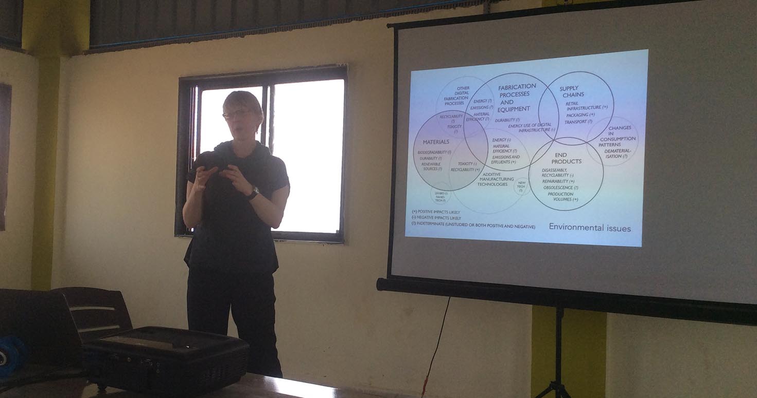
In the end of the day, we had an interesting overview on Sustainabiity in Fablabs by Cindy's Kohtala from Finland, amazing human to interact and share a common topic of research.
Well, thats how my PCB looked after milling till 4am because temperature is too high in afternoons to operate machines in Vigyan Ashram, soon i will be working, sleeping according to Boston time.
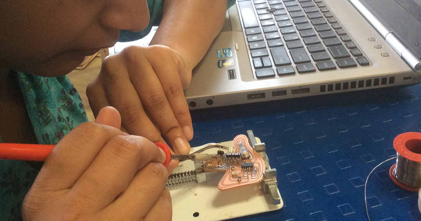
3. Stuffing the PCB
I started my SOLDERING of the following SMD (surface mount) components of the Package 1206:
Starting with:
-1x ATtiny44 (IC)
-1x 1kΩ resistors
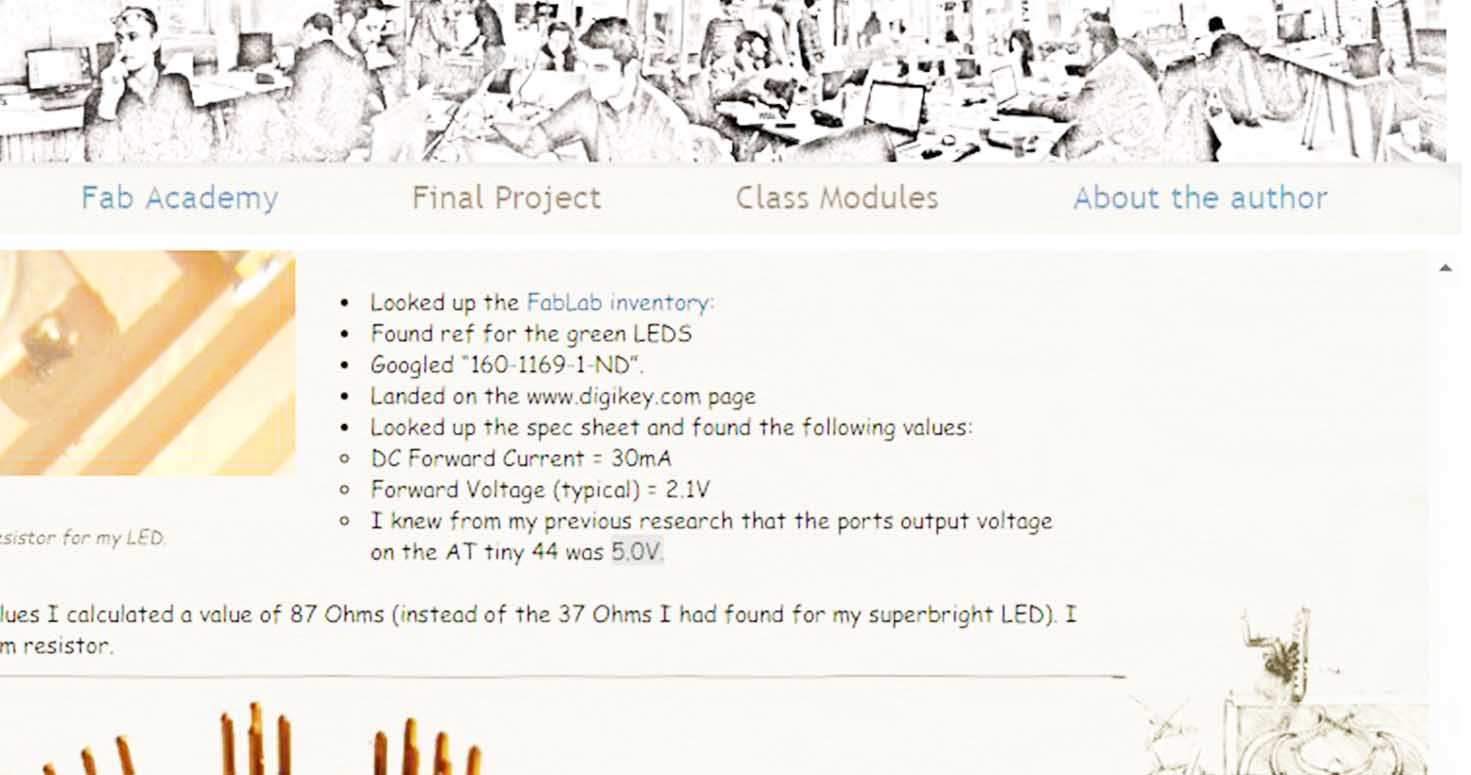
-1x 100Ω resistor
(I calculated resistor for my Led with the help of LED datsheet on digikey, where R=V/I, V is 5V and I is 0.04=125 and 100 was the nearest available resistor in our inventory)
About which i found on this page.
-3x green LED
-1x 1nF capacitor
-1x 3x3 pin header
-1x 1x6 pin header
-1x Resonator
For resonator, i used flux, copper thin plate and then kept resonator over it and used hot gun to get it perfectly synched and connected.
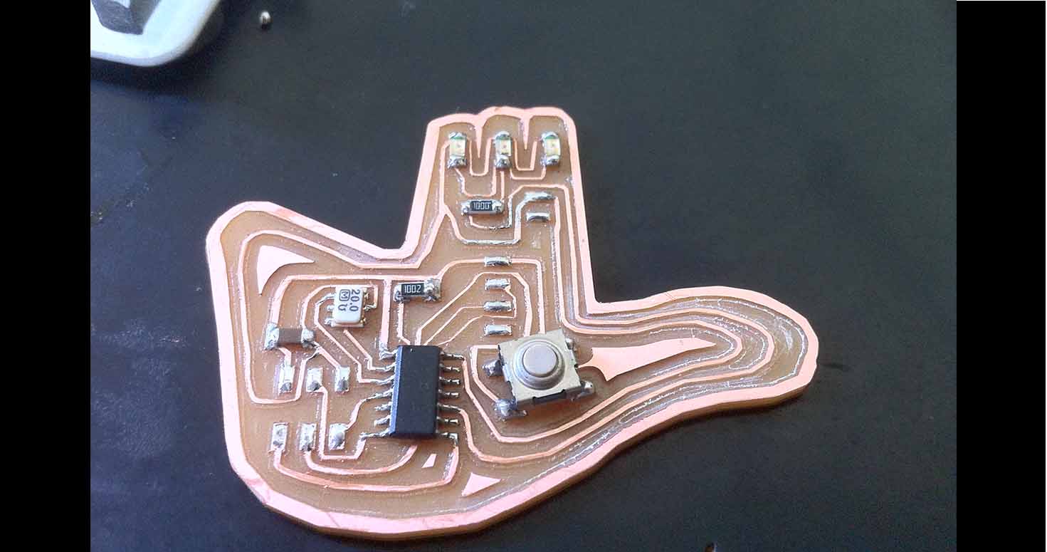
Thats how my board looked :
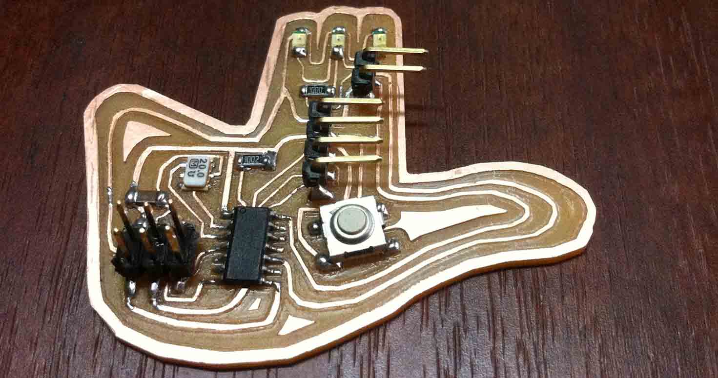
3. Tested my Hello board connections
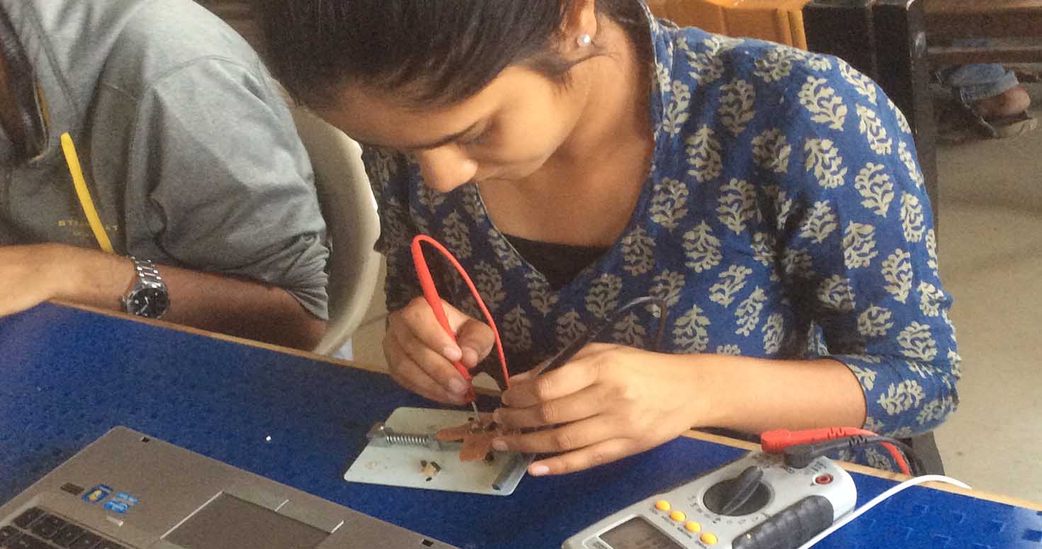
I have used Multimeter to check my connections
Will be trying programming to test it with the help of my Fabtiny ISP made earlier.
Its working can be followed in Week 8
I have learnt and explored existing options in eagle and Rolland which you can find in my Week 13 and in Week 15
Thanks for Reading.
Download Board File of Hello board
Download Schematic File of Hello board
Download PhotoshopFile of customized Hello board
