NOTE: Vigyan Ashram is known as "Fablab 0" , it is one of the remotest labs with very minimal internet access , therefore, we have been using old version of Fab module which is an offline version.
WEEK 4
Electronics Production
Learning Outcomes:
Electronics production is basically aimed at teaching about PCB's, how to design your own PCB's and types of PCB, Machining Process , PCB materials,components and assembly of components, use of fab module and programming AVR in system programmer, as said by Dr.Neil "program a programmer with the help of another programmer to program"
WEEK ASSIGNMENT: Make an in-circuit programmer
USING : UBUNTU 16.4
1. Introduction of PCB Fabrication
I have used Roland Modella to do PCB milling of FR1 PCB material.
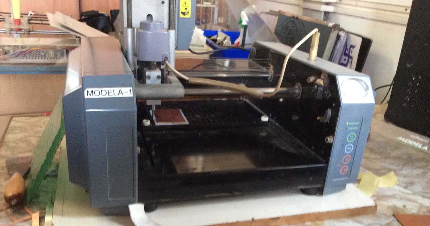
There are 4 actions which can take place in this machine like PCB tracing, cutting, Wax cutting and Wax molding.
So for this week our focus is to use it for Milling our PCB.
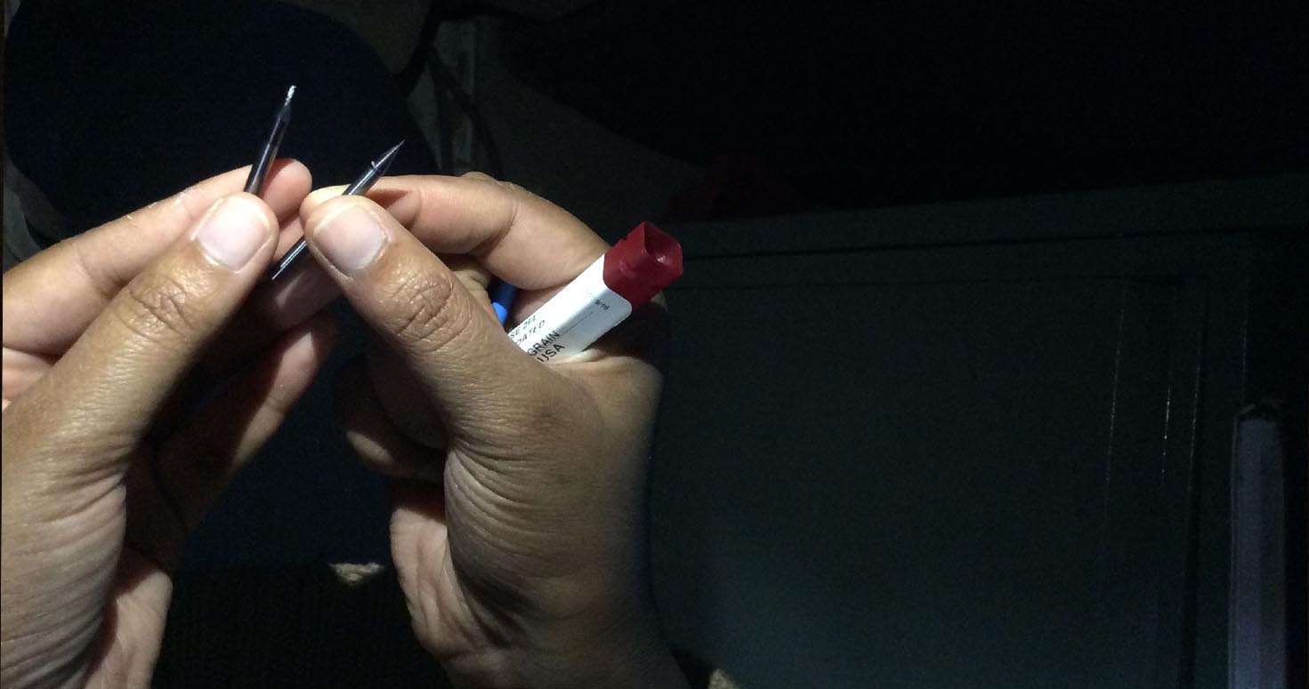
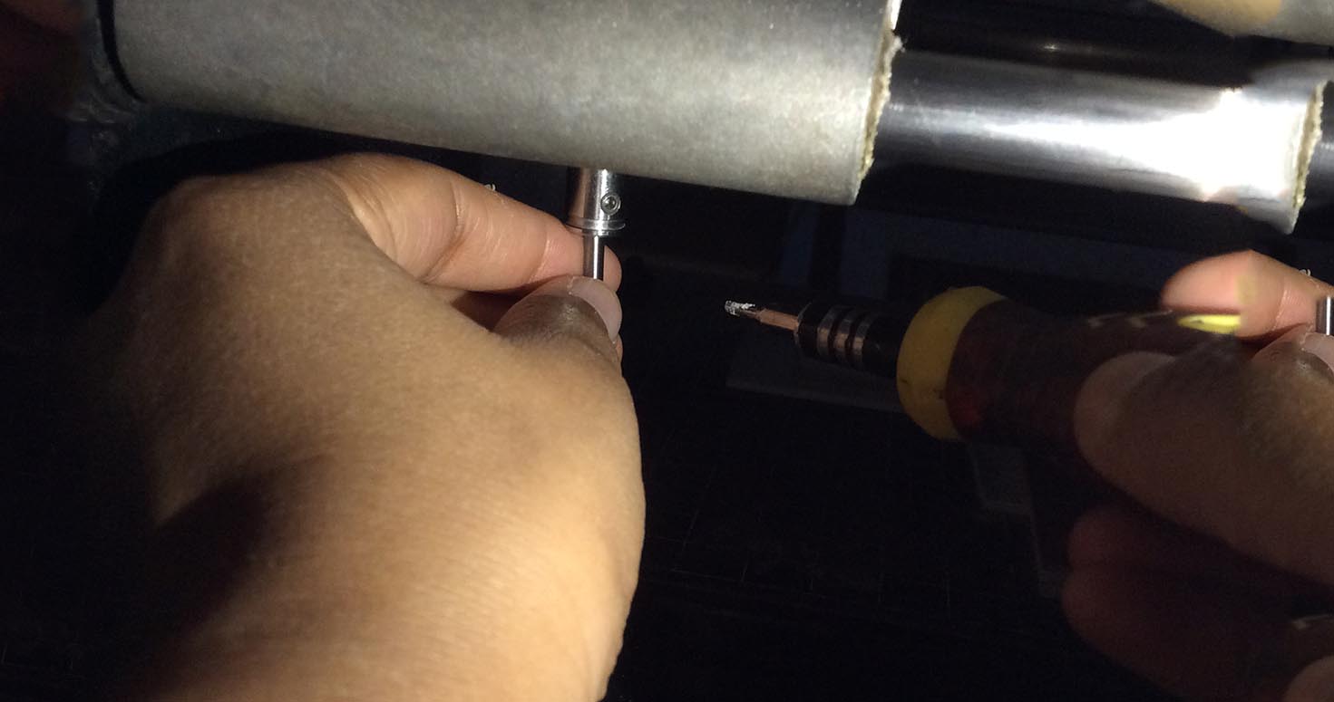
I used two types of mill bits ,
Below is an image of close up of these two bits. The sharper one is for tracing and other one for cutting.
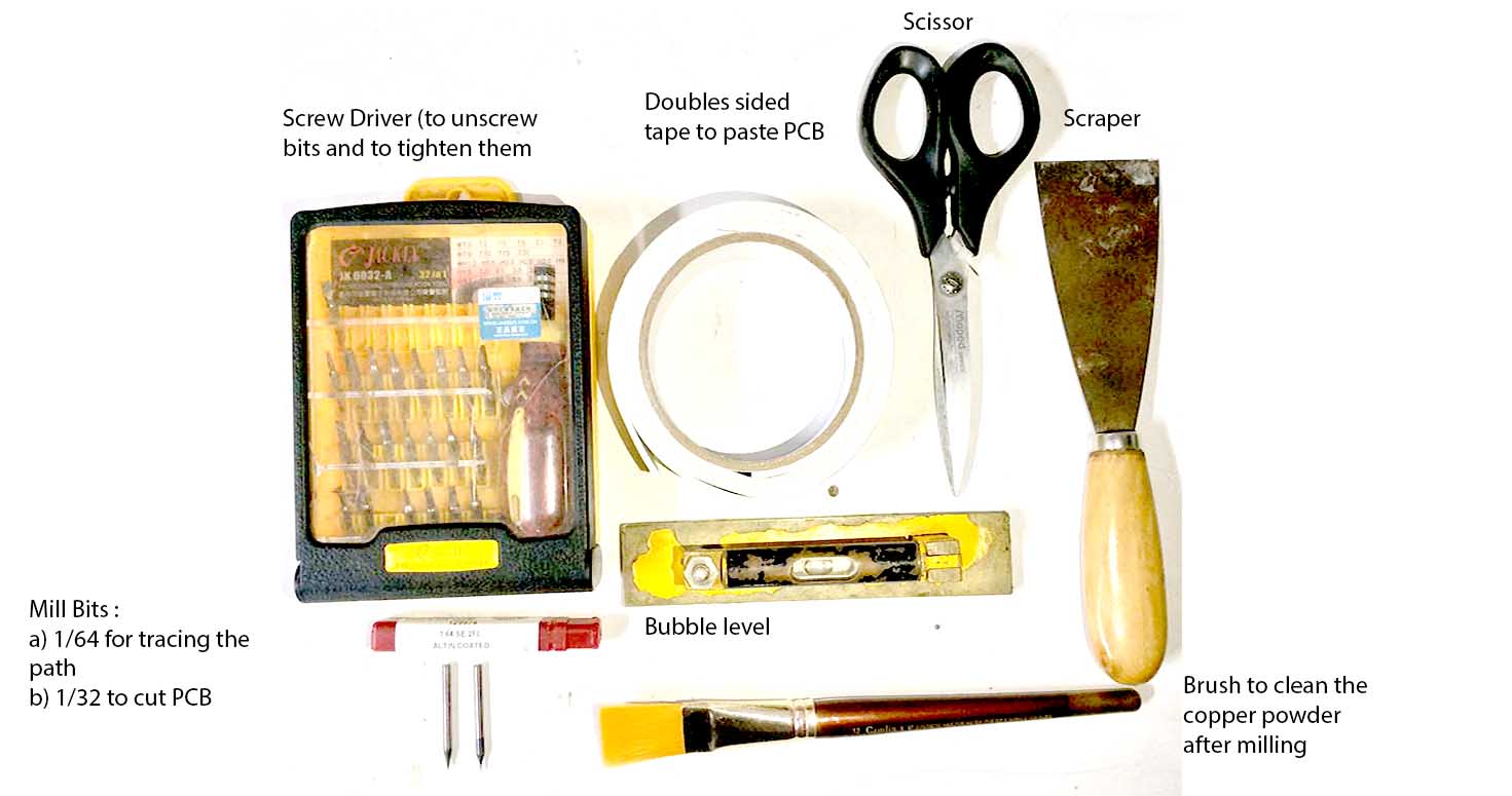
Other Materials used in the process of Milling:
The good thing is that i did vinyl circuit in my laser cutting so i had clue about Eagle, circuit basic processes.
We were given a very interesting and very helpful introduction by our instructor suhasji on first day itself explaining about electronic production which went ahead as a very useful discussion among all the fabbers, joined by other members of the ashram.
It was continued by our another instructor suyogji who explained us the working of the Roland modella, milling bits, settings like overlap, depth, offset etc and functions.
We were also shown different components like resistors, capacitors, diodes and their functions because i am a beginner in electronics so it was a must for me.
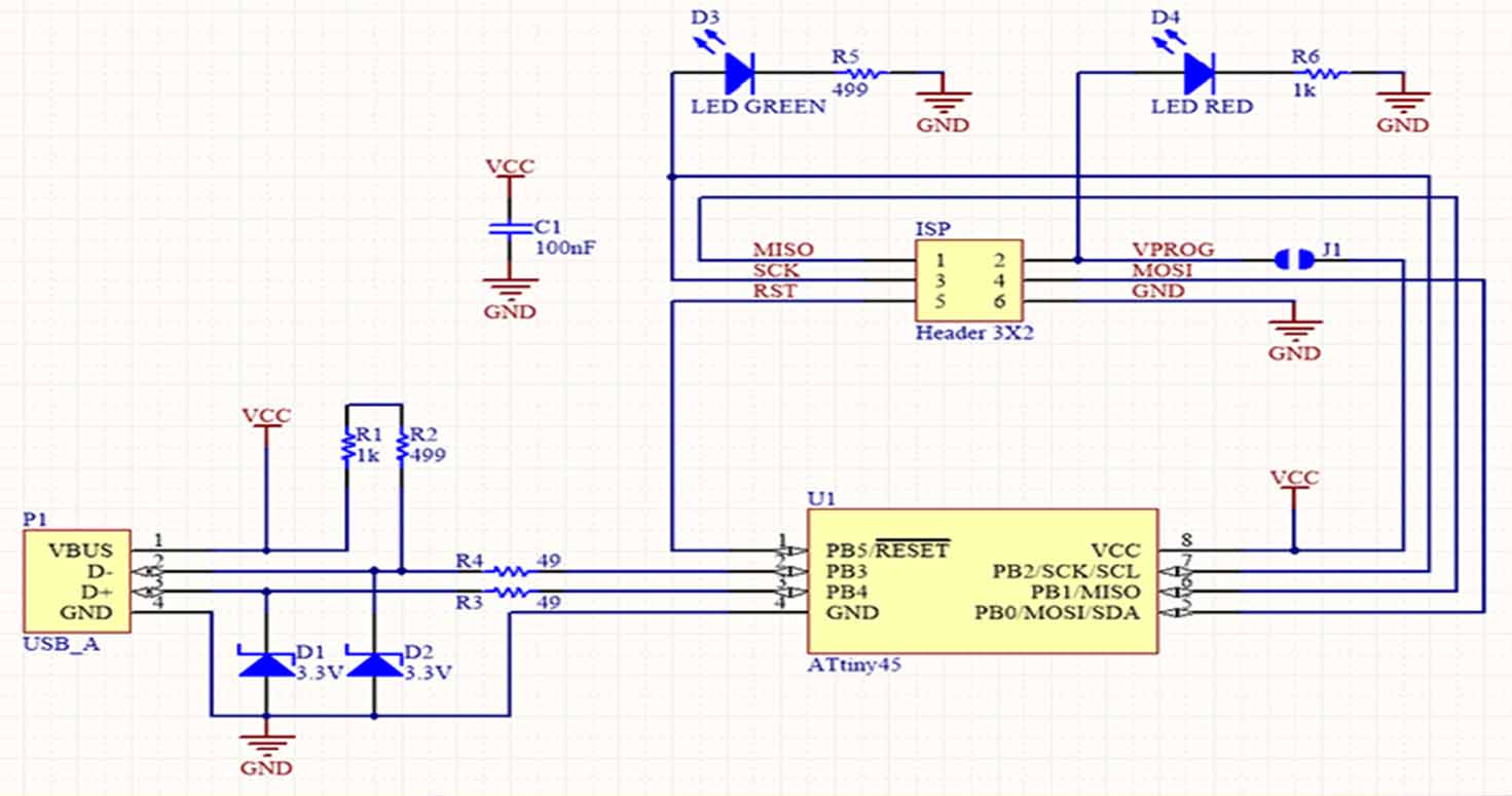
I continued reading further by visiting Fab academy resources and different ISPs(The FabISP is an in-system programmer for AVR microcontrollers, designed for production within a FabLab. It allows you to program the microcontrollers on other boards you make) -Electronics
Read about different ISPs made in fab academy by other people like Davd, Brian, Ali, valentin, which led me read about the experiences of other students with these ISPs.
Went on to see Modella tutorials to understand the right way of handling the machine, its settings, its precautions. Please Make sure to keep it close when running, and clean it after use. Most importantly dont forget to switch it off after use.
I chose Fab-able Insystem Programmer (ISP) by David as my AVR ISP programmer.
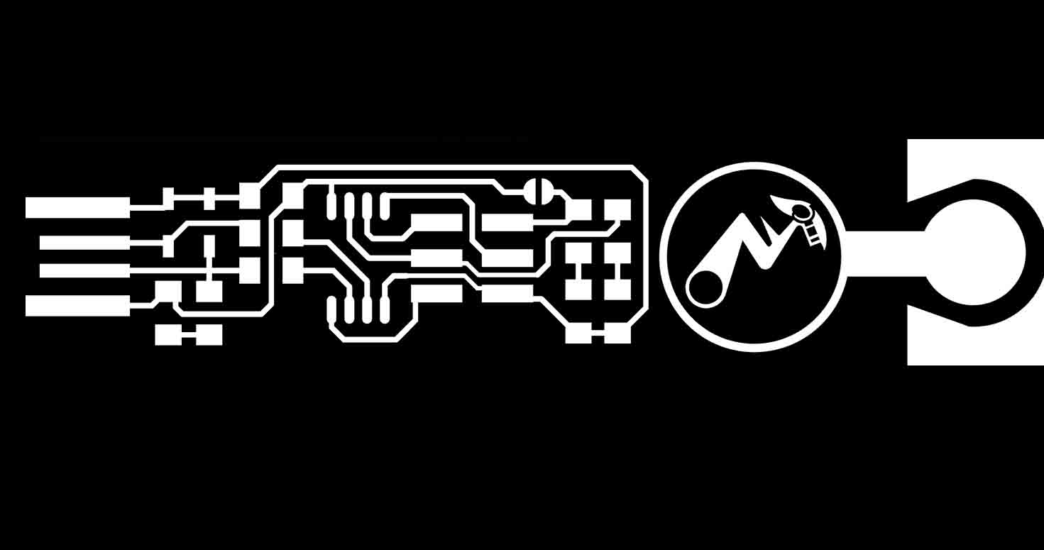
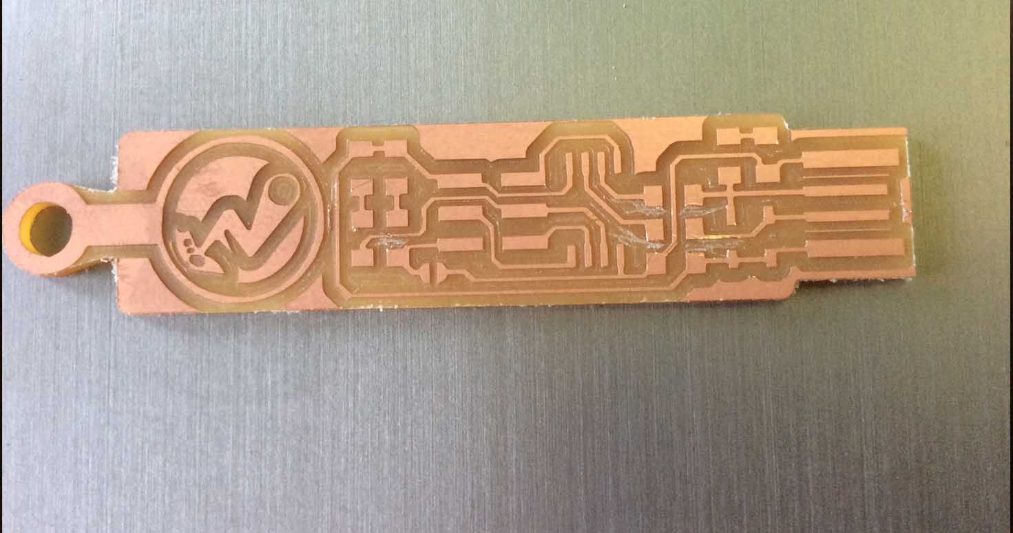
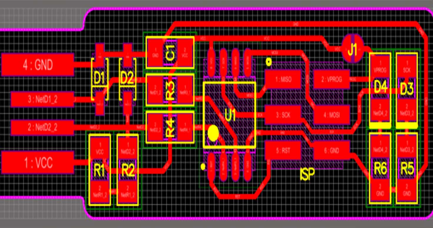
I edited the ISP's Png in photoshop where i added my company's logo , changing the outer shape and extended it further to use it as a keychain or necklace piece.
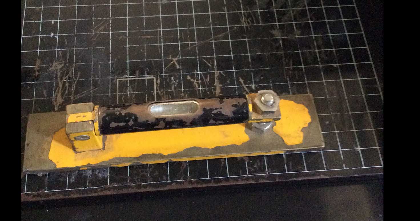
I used bubble level tube to check the level by keeping on flat surface first and check the position of the bubble and then keeping on the Modella plate to see if the bubble is at the same point. Well, bubble needs to be in the center but it seemed that this one had some alignment problem so i checked by keeping to the surface and same position should adhere to the Modella base. This means your plate is flat.
I started with milling with FABISP of David's , redesigning it from outer.
I went on Milling my Ist PCB with the above circuit design with the help of fab Module.
Following steps for milling on fab module:
a) Open terminal
b) Type Command
sudo fab
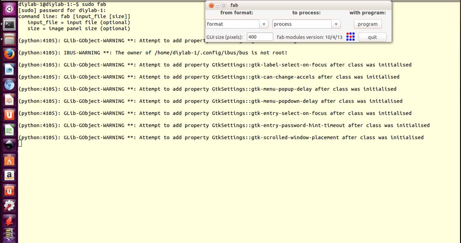
c) Fill Password
d) Select png as format and Roland Modella
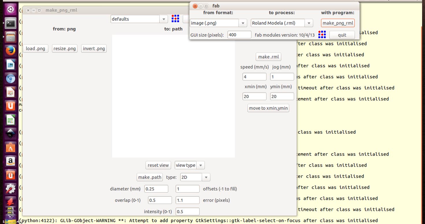
e) Load png ( If you are milling then 1/64 bit and if you are cutting then 1/32 )
f)select make path, (choose x and y axis)
g) Make rml and send it
h) Happy Milling
NOTE: Make sure your x-y axis, view type, type, offset are right.
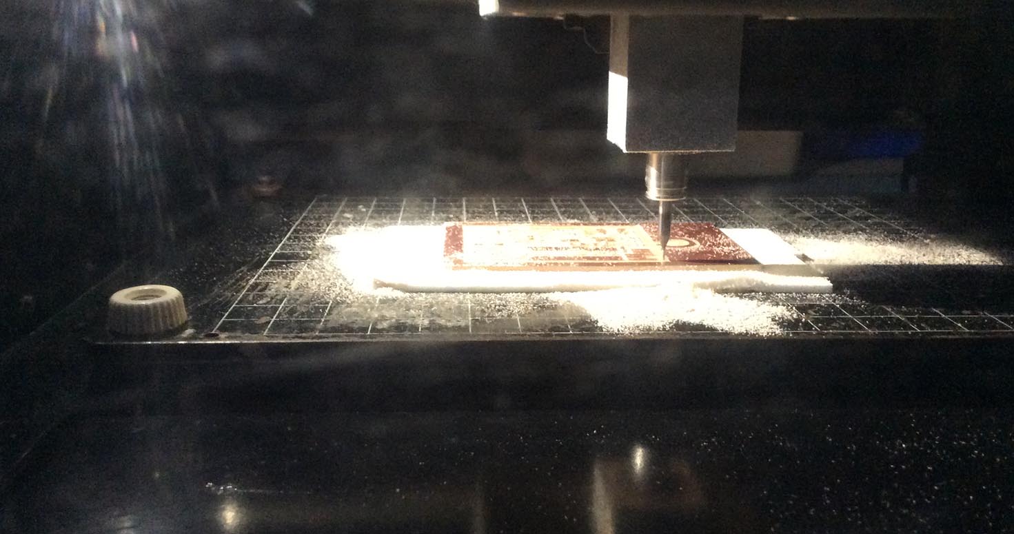
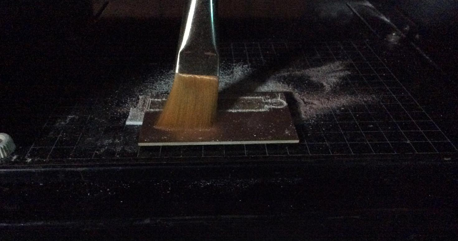
I started by pasting my PCB with the help of double sided tape on the modella plane. Make sure you paste parallel to the x and y axis.So it becomes easier to track the origin on fab module.
Also, Make sure you press it hard with equal force all over the plate so that when mill bit runs it gets a flat surface and surface doesnt move if the force is applied by the bit.
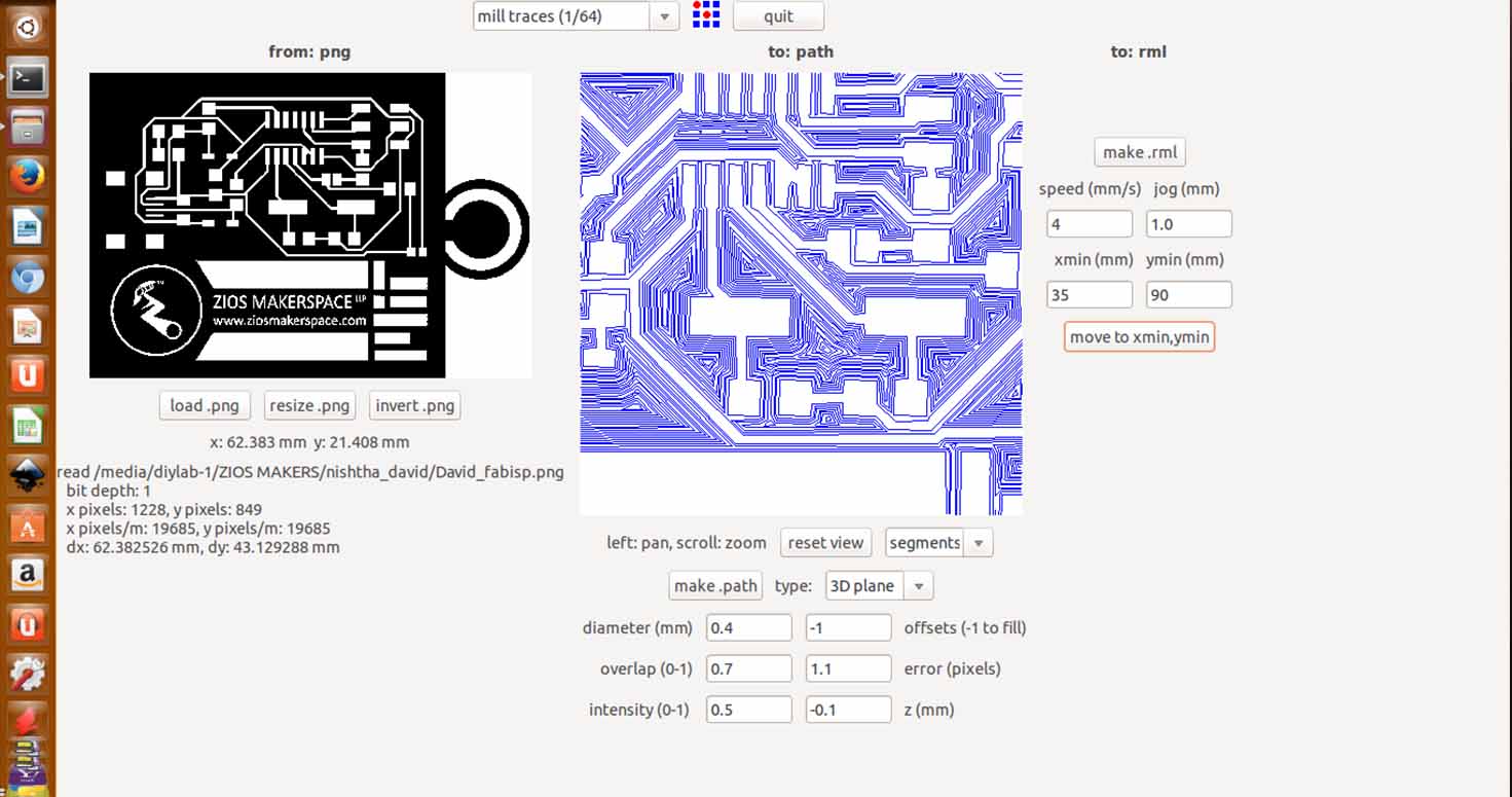
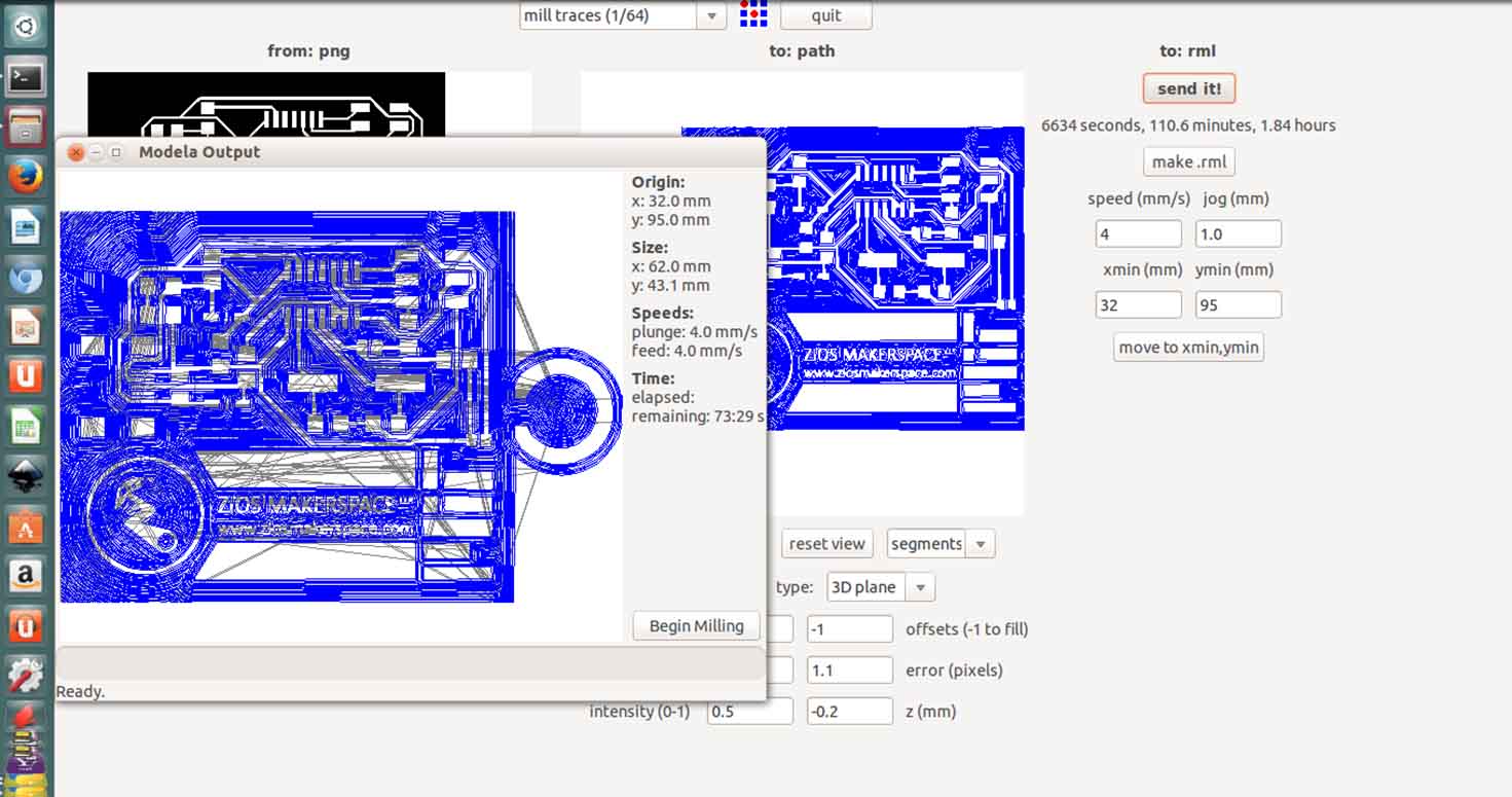
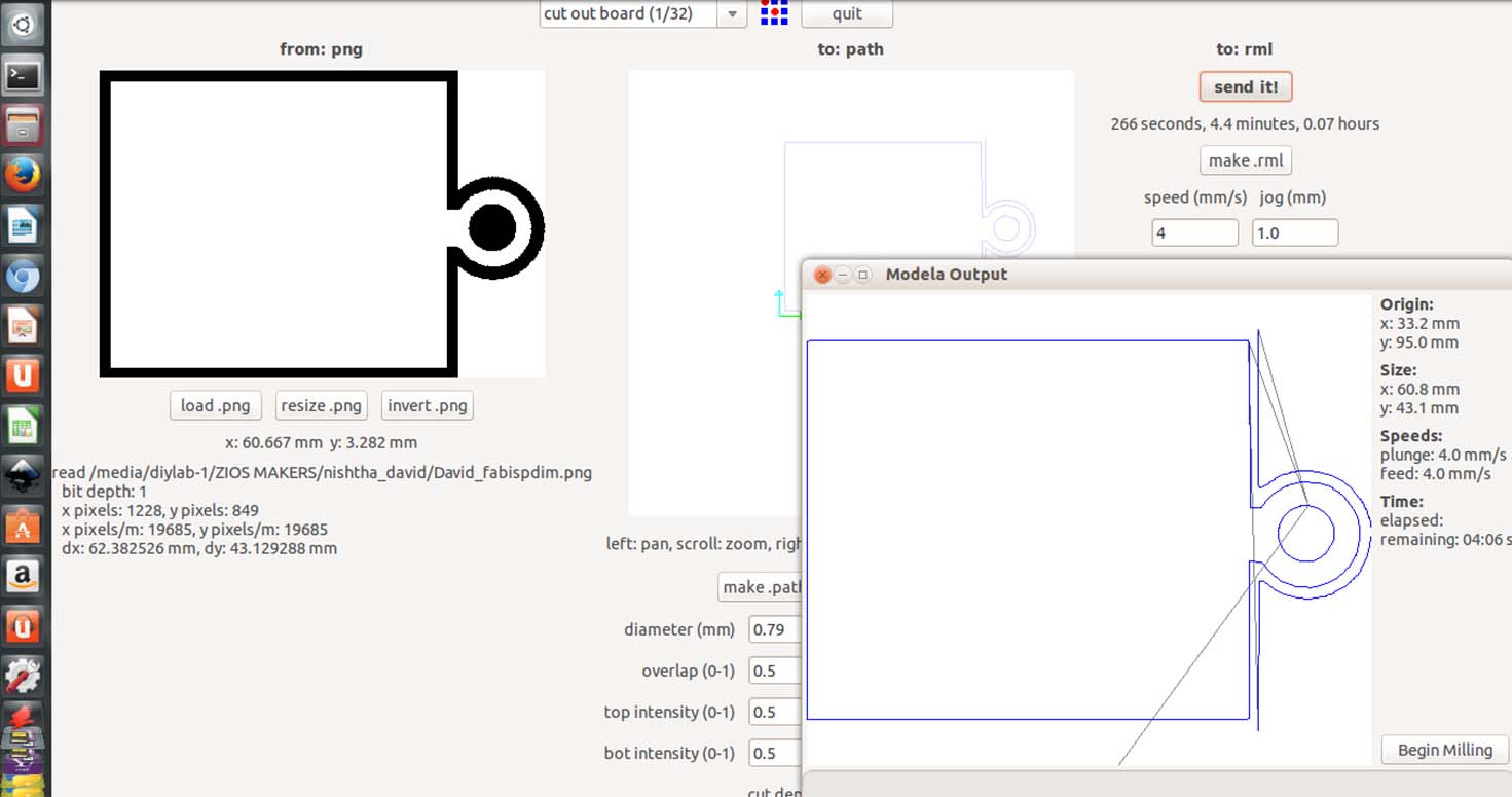
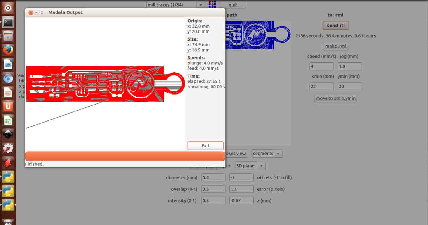
I took this shot because it explains perfectly the origins, size of my design, speed and estimated time. Also, make sure your design length and breath fits the PCB and doesnt come out or doesnt waste the PCB board. Printing the Traces of my ISP with Mill bit 1/64.
  TIPS for 1/64 traces:
 -In case you dont see the path coming completely, decrease the diameter point wise because sometime the width of the path is very less or more than the diameter of the mill so you have to change its diameter to get your full path.
-Change z to -0.6 from default , i did that so that my milling bit mills only the copper layer and not the plastic below it because that plastic which shreds tampers with the path while milling.
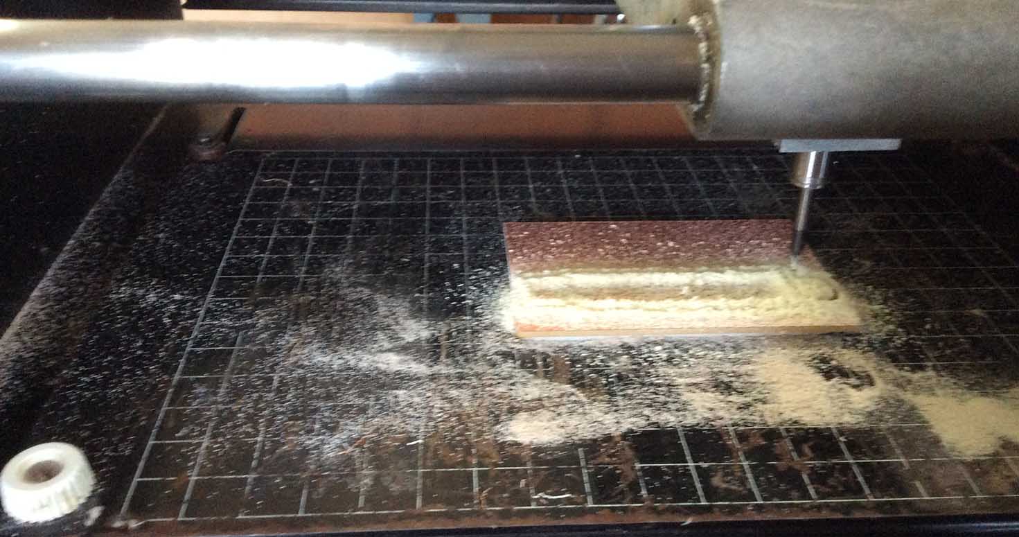
Now after traces, I cut the frame , for which I had to change my mill bit to 1/32. Well , unscrew the 1/64 bit, put this one, tighten up. Now when you are putting 1/32 bit make sure to put it inside properly leaving only the tip outside. Also, after screwing it well, you can use down arrow on the modella to move the axis downward. After that hold the bit and gently drop it to the ground that it touches the surface properly. Screw it .
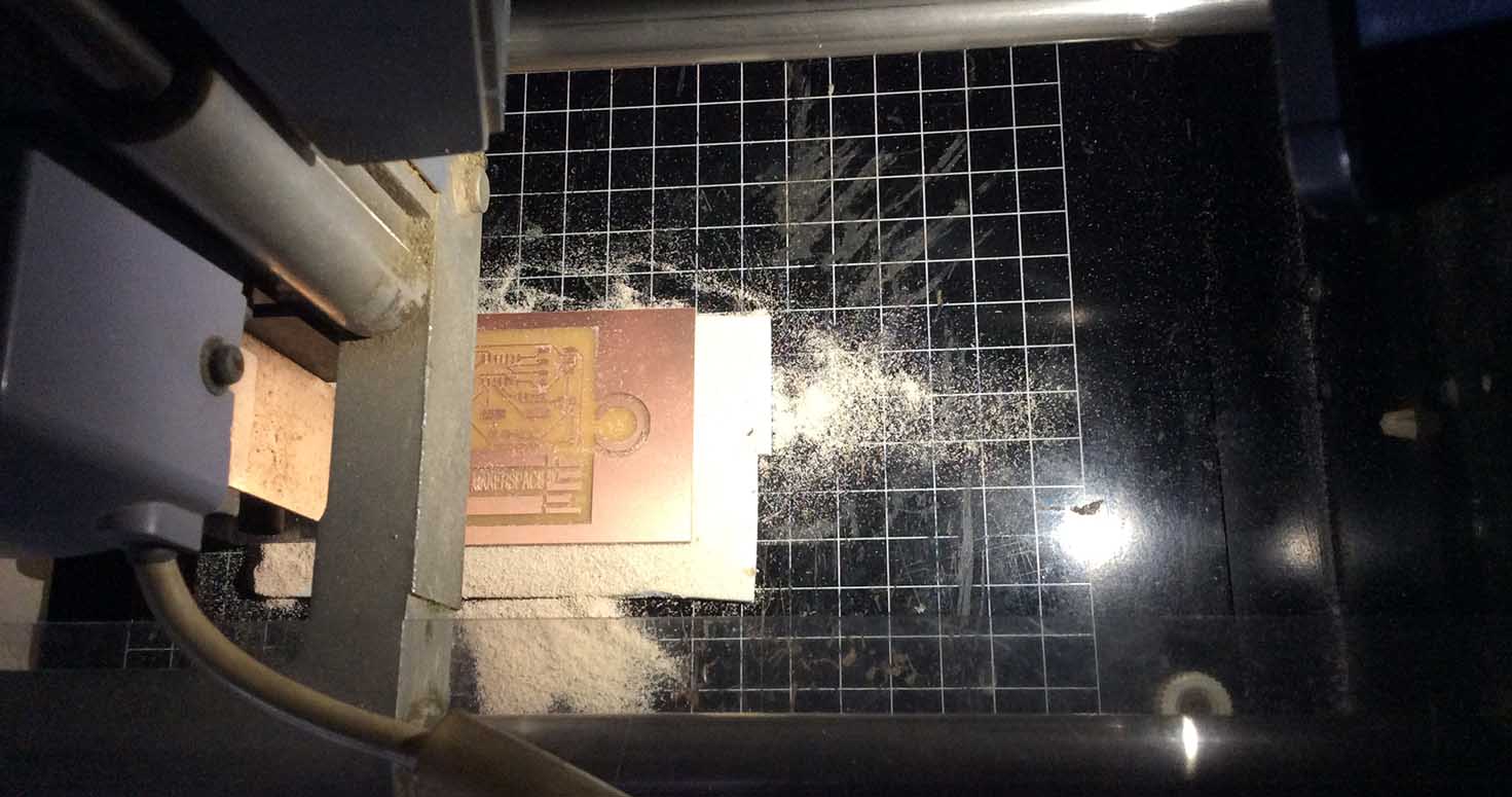
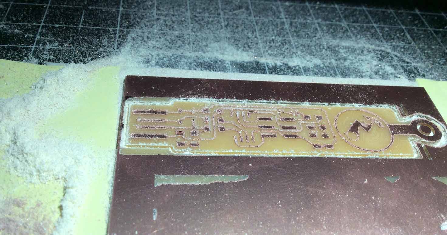
Continued cutting it with 1/32 milling bit, I traced first and then did frame so that traces surface area is enough to mill , because smaller the surface area , more probability of the movement of the PCB.
I did corner to corner printing because of the size of my design i.e 60mm and 43mm
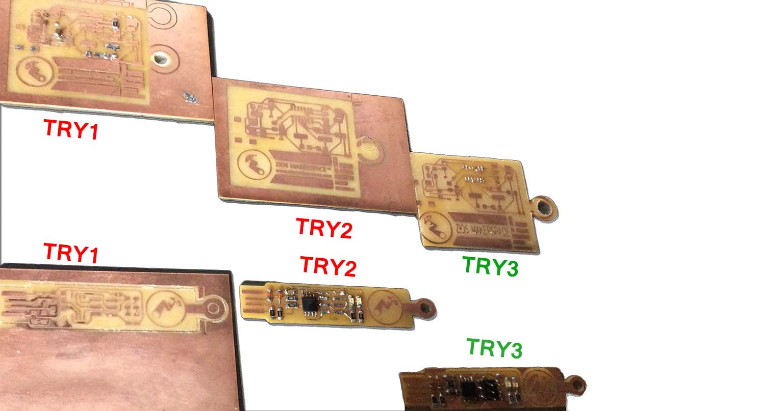
And it turned bad, procedure was perfect,after completing one design it was overlapping another design over it. So probably its the problem with my design or machine.
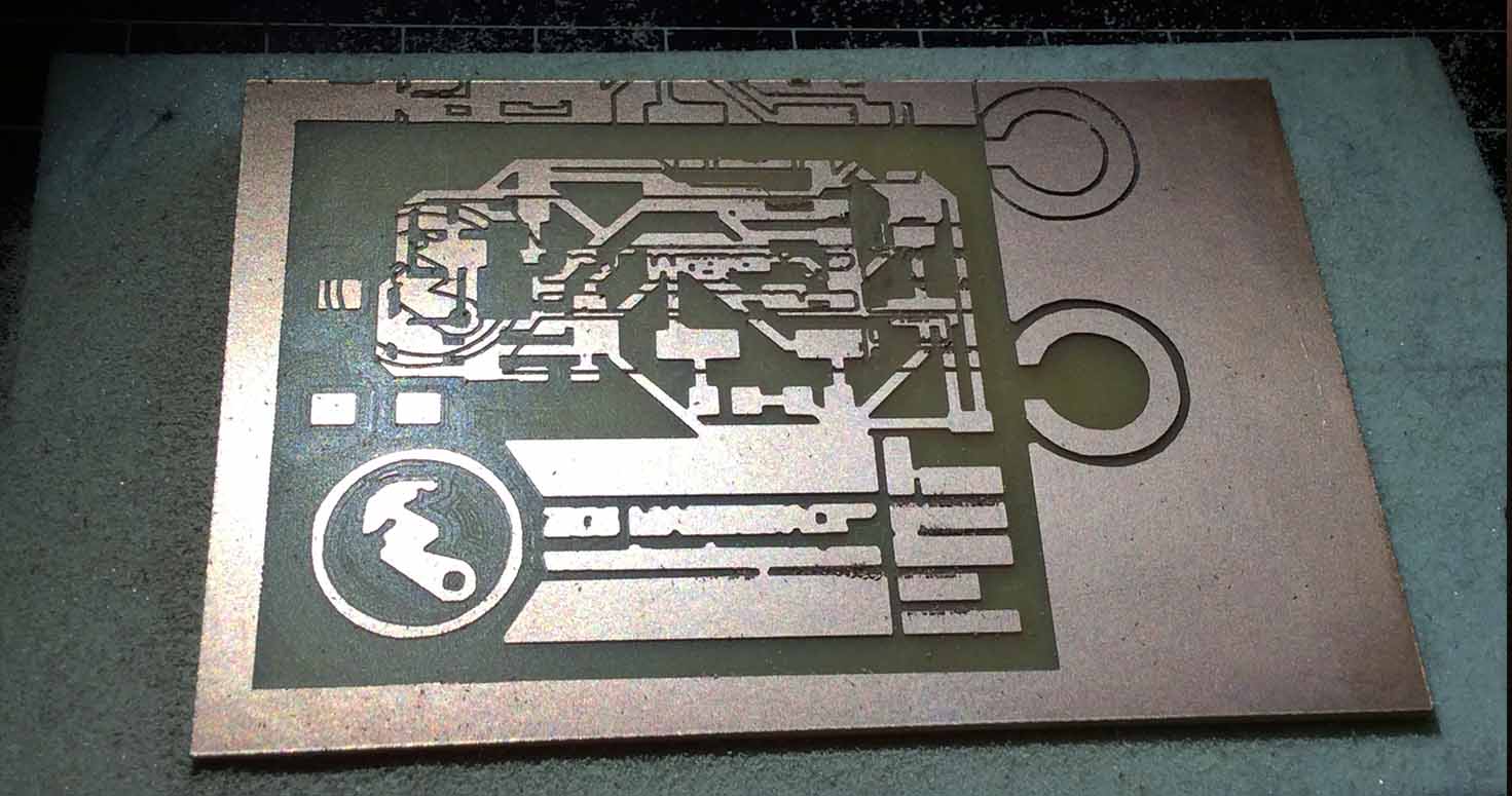
So i decided to try again IInd PCB , and it again started to do the same thing, I stopped it, tried different settings, gave lot of trials with offsets and other settings.
i felt probably its because of the design, so I chose simpler design which was well documented too that is FabTiny ISP by Brian and edited further like i did David on photoshop, adding some design to it and milled it, IIIrd PCB
STEP 1- Open Fab module and select the origin and offsets
STEP 2- Make sure you are away from the modella and not putting your face inside to look it while its milling.
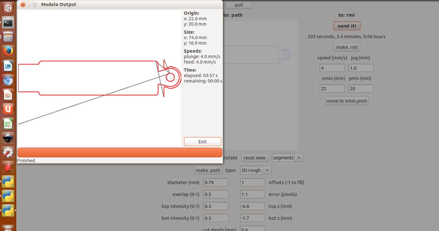
STEP 3- Then I went on cutting my frame.
Later while I was milling, it came out that there was problem with the machine as it was giving incomplete traces. After checking i saw that a small bit of the screw driver was stuck under the milling plate which made it shaky.
Well, it again didnt mill well, it gave me incomplete path , means some of the joints of the path were missing.
While it was milling, i tried my hands on soldering the SMD components. I was able to solder IC on my previous Brian ISP to practice.
Well, i was getting impatient because of delay in my work but then came sunday and few of us planned to go out as it was birth anniversary of a famous Indian warrior king Chhatrapati Shivaji Maharaj and few employees of ashram invited us and this festive is celebrated across the state with lots of vigour. So we went to visit a fort where he took birth.
Visited Budhist caves and beautiful temple. Though it was very tiring because we climbed unknown numbers of stairs and did lot of trekking and went on bikes for about 100 kms but it was surely mentally relaxing with amazing group of people.

So today is monday and suhasji tried again and it gave a very harsh and incomplete milling, i got very demotivated but then i was counting on my instructor to figure out the problem with the machine because i couldnt.
Well, he cleaned the machine base, pasted a new PCB, reset machine settings.
This time we were able to print by using new mill bit. that is my 5th PCB.
2. Tinkering with electronics
Tools i have used while soldering:
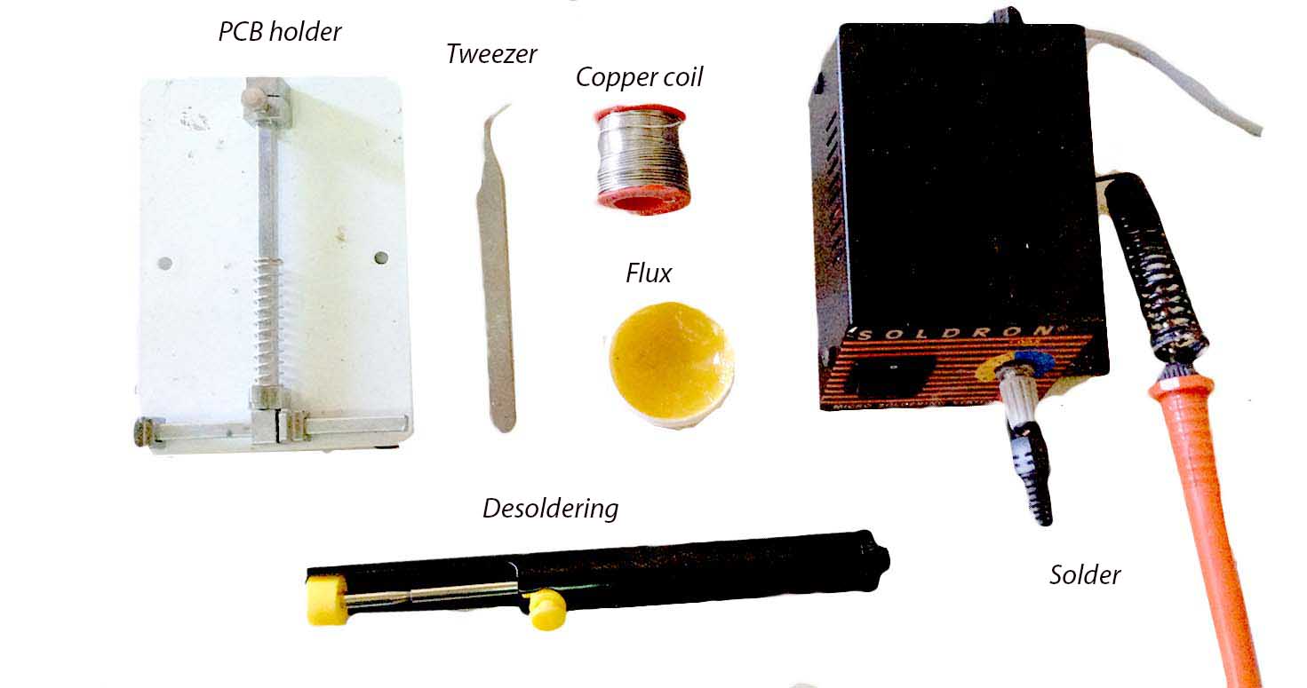
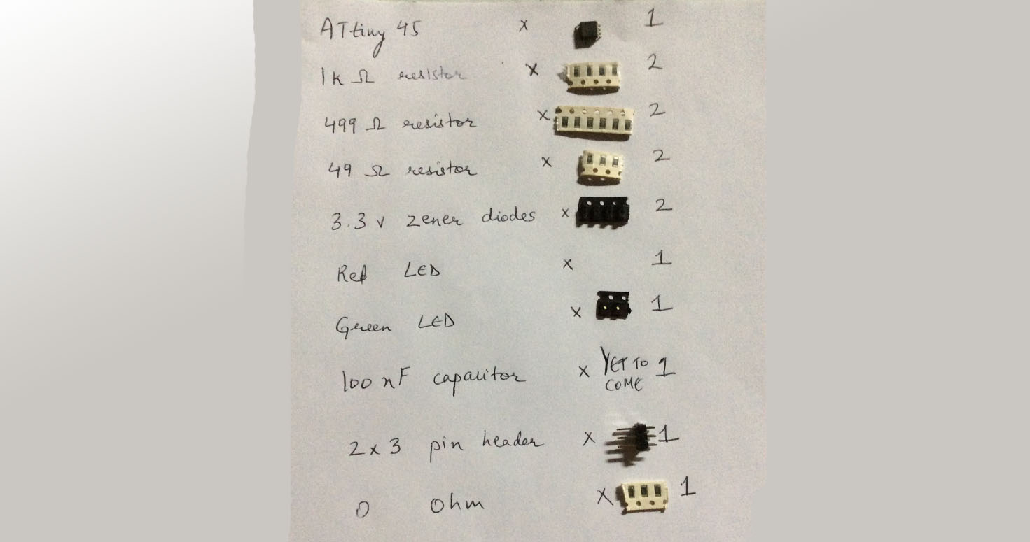
I started my SOLDERINGof the following SMD (surface mount) components:
While you collect your components, I feel this was helpful for me to write down the components and how many you took because not every component has name written on it , making it difficult to identify later.
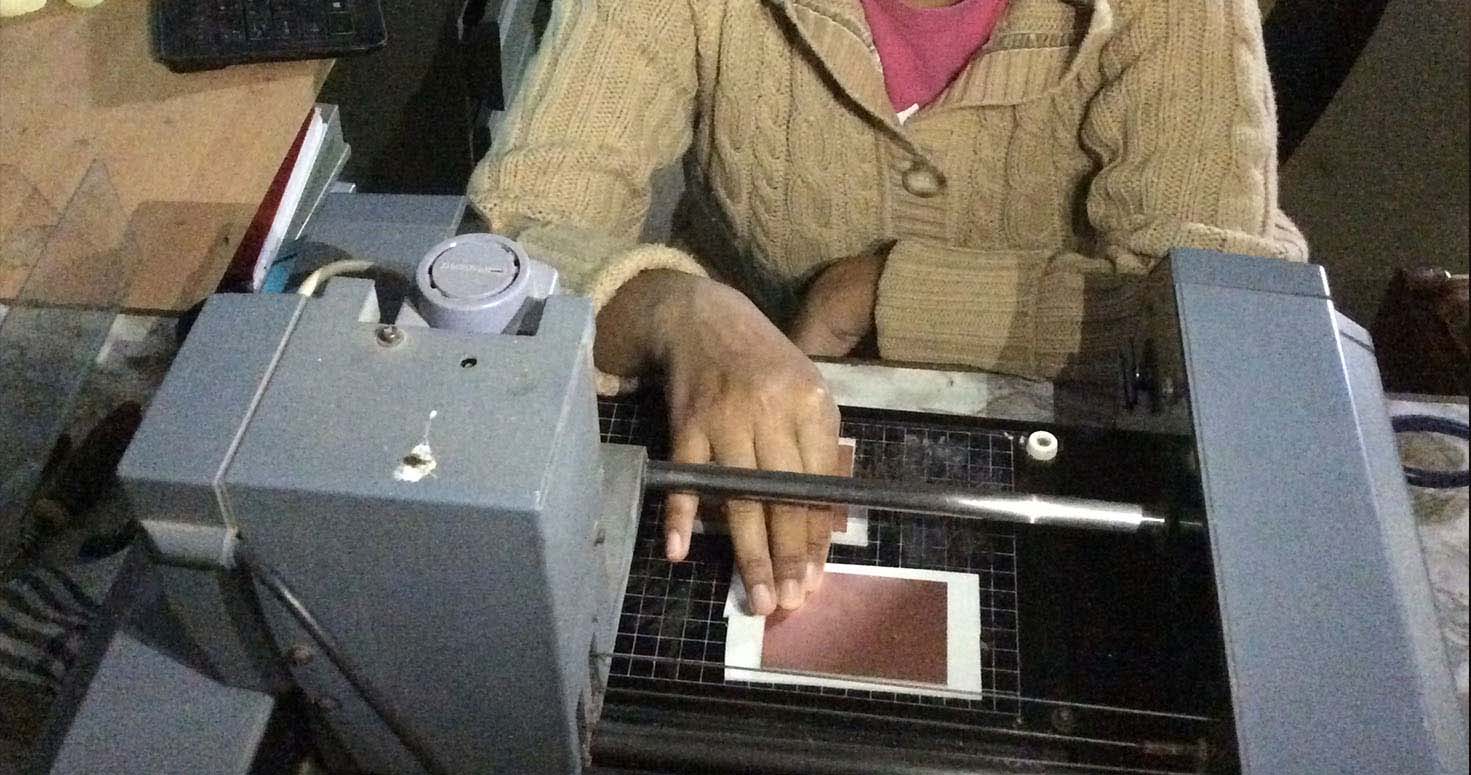
Below image, was my first try to soldering.
I started soldering the IC first with the help of flux, soldering copper, soldering gun, tweezers.Make sure your two points are not in contact untill unless required in your circuit. Keep checking connections with Multimeter.
  TIPS for Soldering: I dont know if it stands true for others soldering too, try and have your best way

- Put a thin layer of soldering copper, then put light flux and put your component and a drop of copper over it.

- Make sure you hold tweezer in a comfortable posture

- Take deep breaths and do this with focus , keeping your board file in front for referring
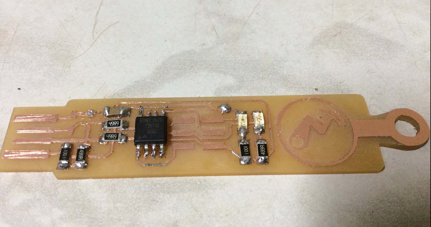
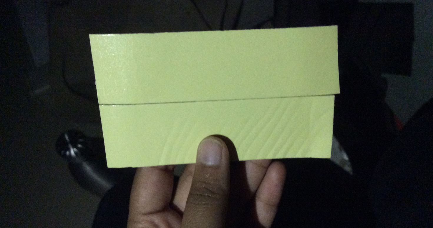
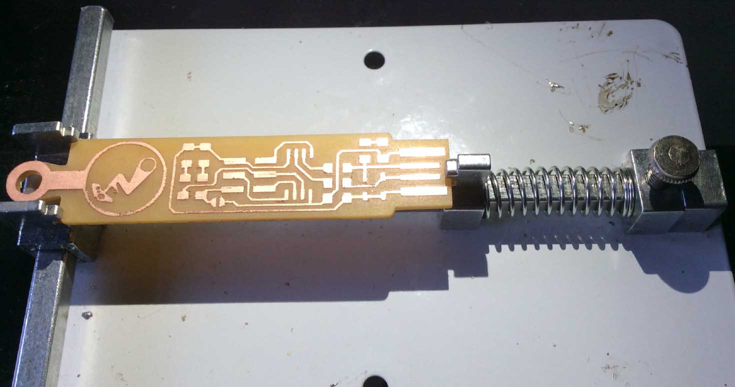
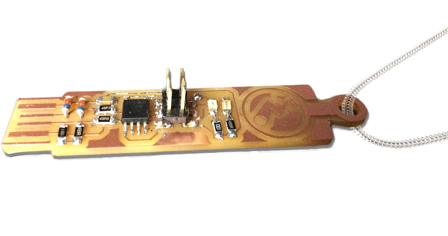
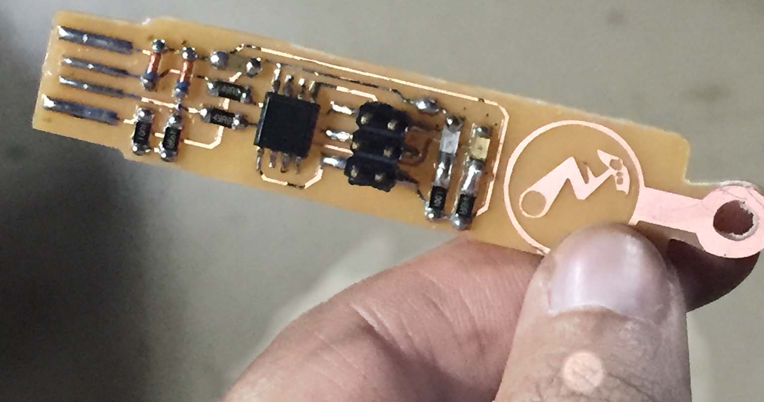
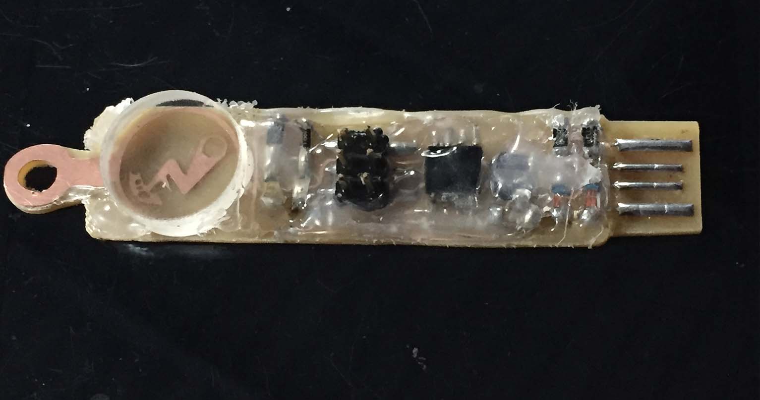
My Finally Milled-Soldered ISP which can be used as neck piece too keeping my first ISP safe and handy to use.
Below are my trials, which later on realised was errors in the machine either caused by loose USB connection with the Pc or due to power cut while it was milling or due to bit exhaustion, All my trials:
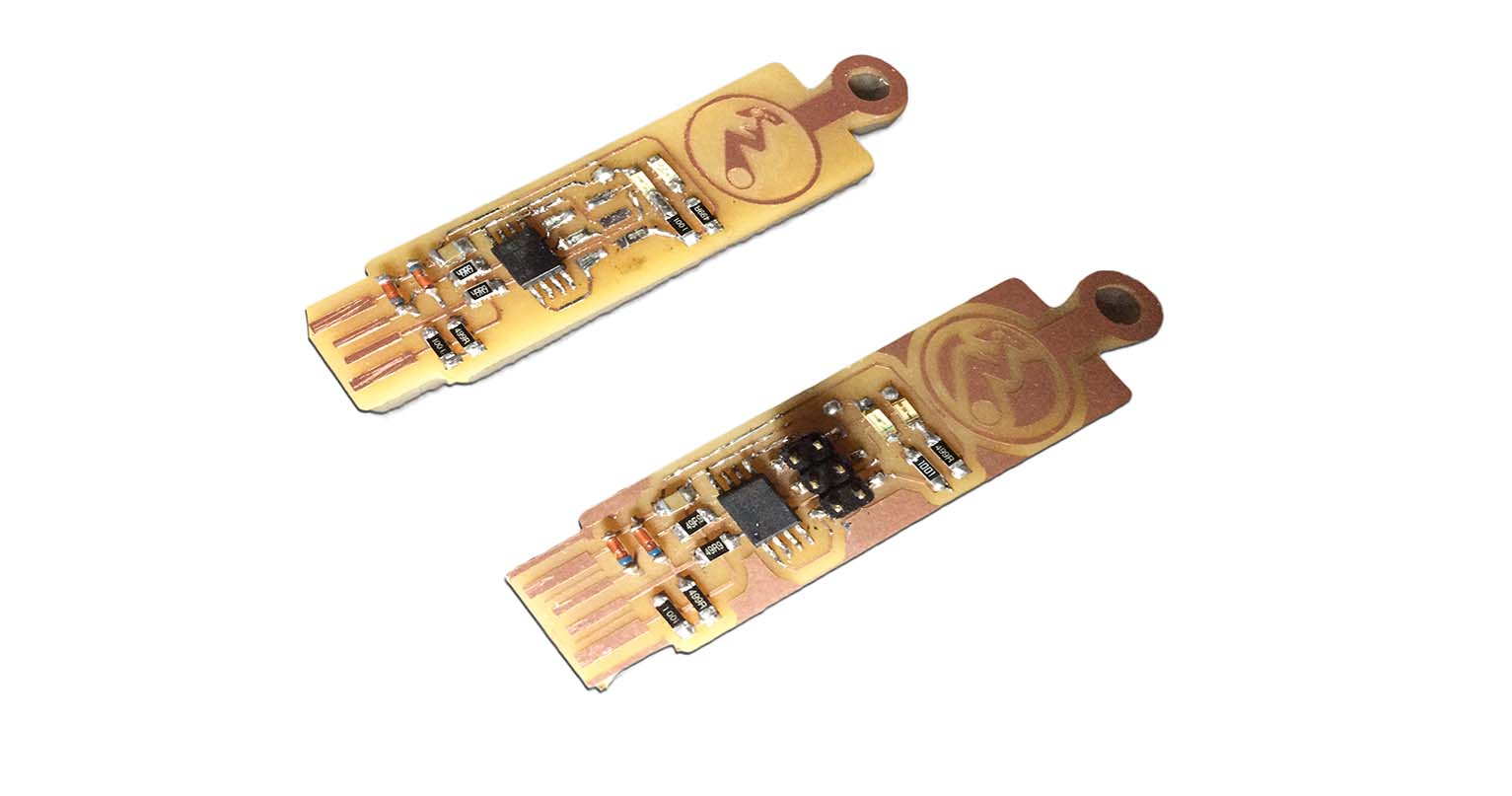
Now i had two Brians , One on which i practiced soldering and other one which was my final milled and soldered. My header came off while trying it for programming with jumper wires. So its missing in my first trial of ISP soldering, i did connect it again.
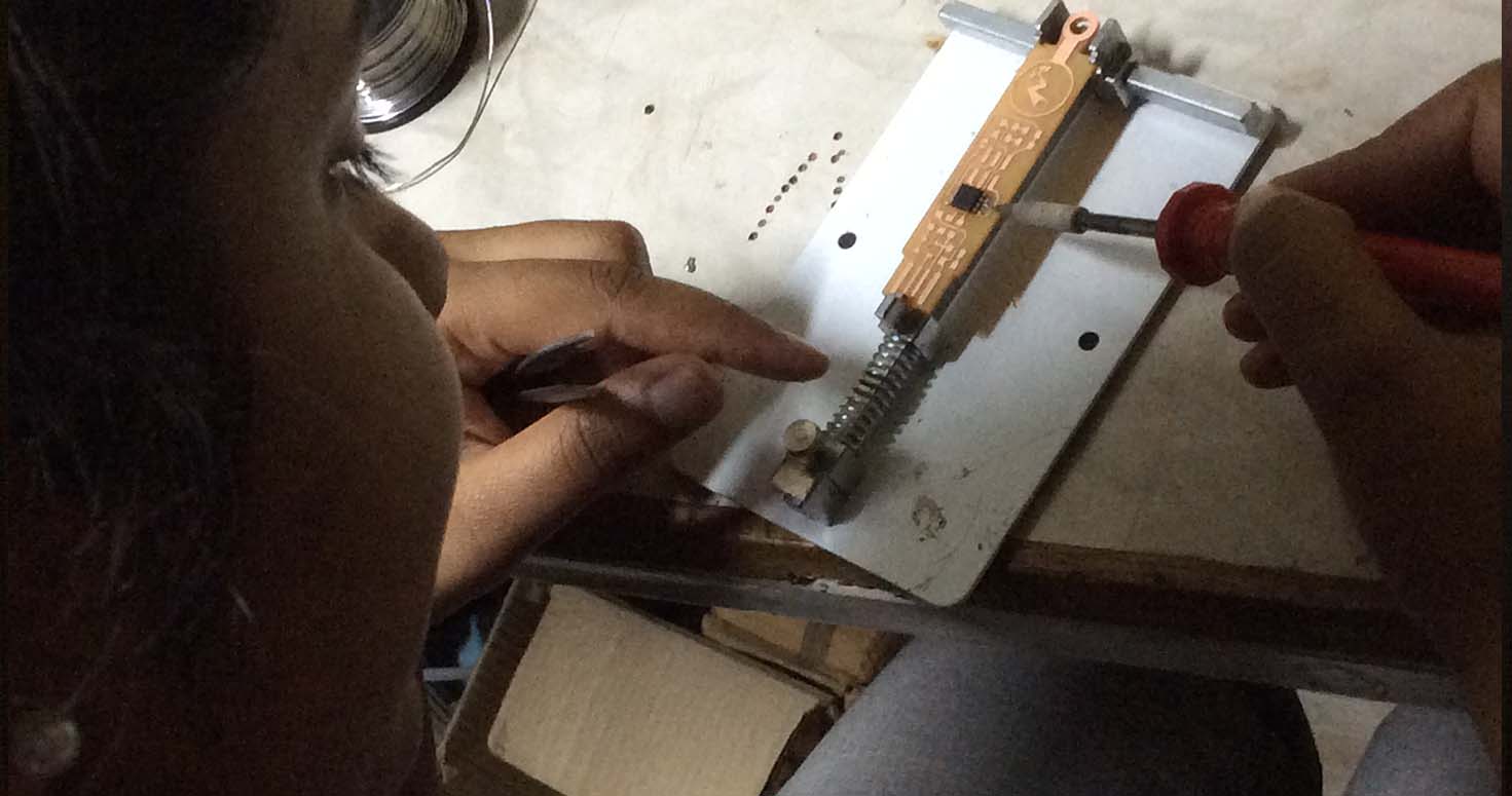
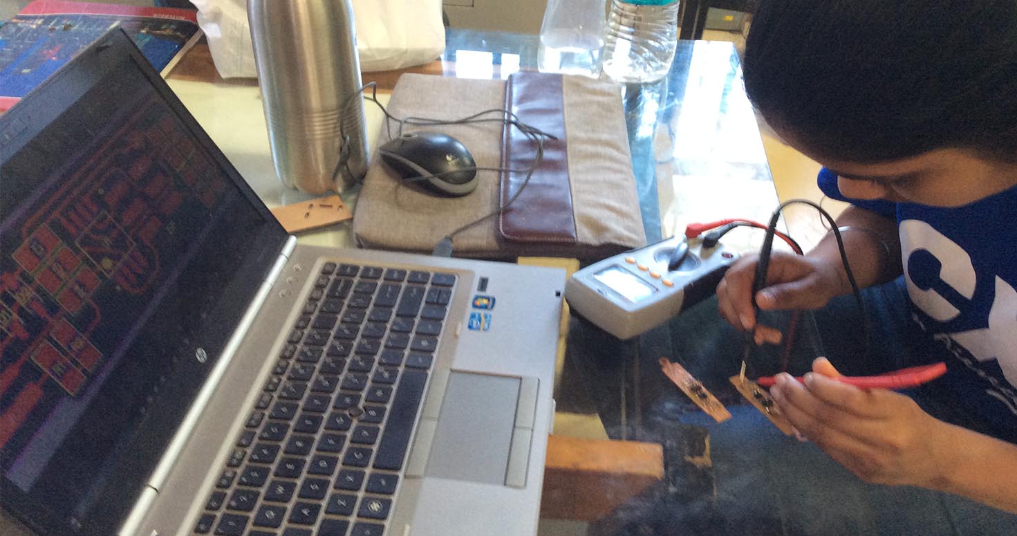
Checking my connections with multimeter of both my ISP's (I checked with multimeter after placing every element so that I am not stuck later)
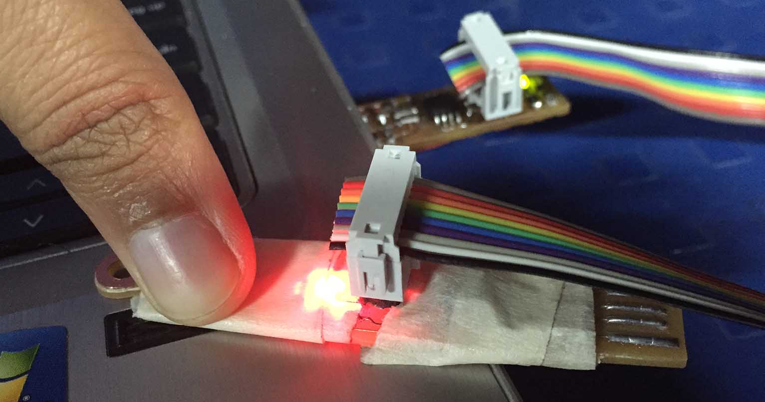
SMOKE TEST- It is to test if Pc even recognises your ISP as any input.
I did smoke test of both my ISP's the one on which i practiced BRIAN first try and BRIAN my final ISP.They both showed this message when plugged in to my laptop.
3. ISP Programming
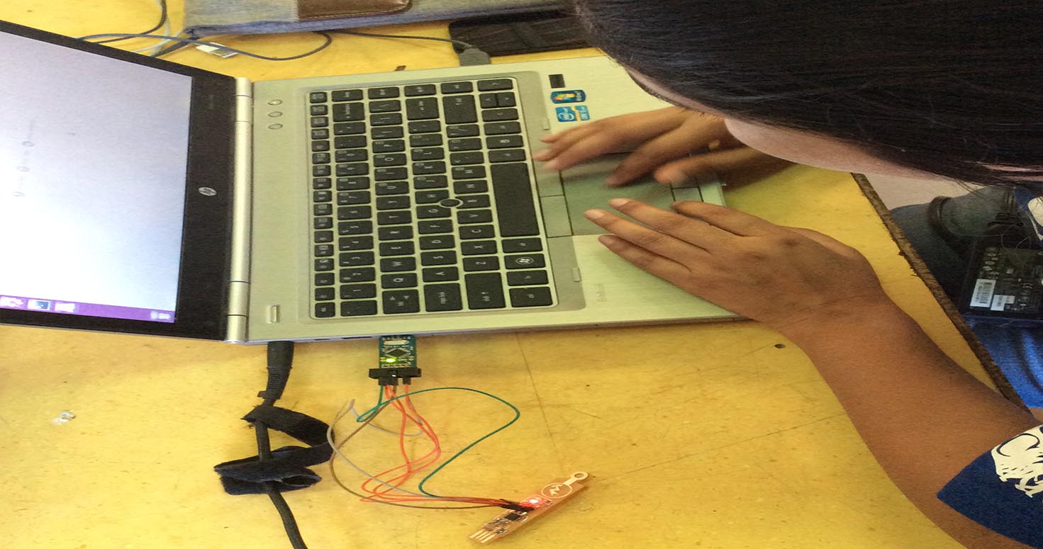
I went on further Programming my ISP with the help of USB asp programmer.
So first I connected the jumper wires from my ISP Ic to other programmers' ISP.
Matching: MISO to MISO, MOSI to MOSI etc.
Refering this image.
Though i got stuck 5-6 times after unzipping, but then i was able to succesfully program it after checking my boad conenctions again and resoldering few points, so writing the steps.
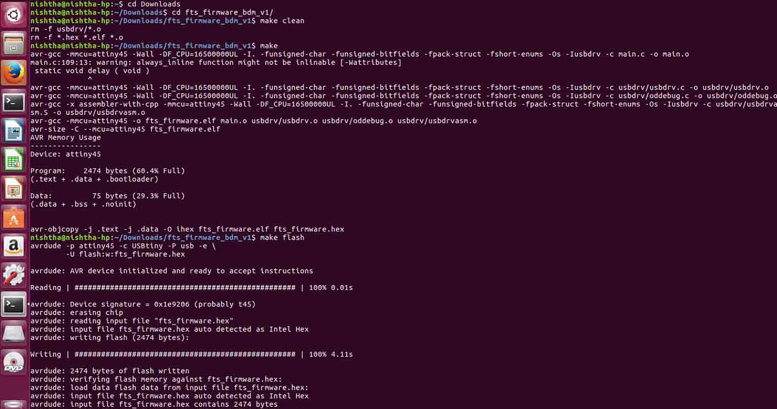
1. For Ubuntu, enter the following command, followed by your password when prompted:
sudo apt install avrdude gcc-avr avr-libc make
2. Download the firmware source code and extract the zip file (on Linux, unzip fts_firmware_bdm_v1.zip) and shift the folder to the Desktop.
3. Open your terminal program and give command
cd Downloads
Type command:
   cd fts_firmware       /click tab to select folder

   cd Fs                 / click tab it will show the file name

   sudo make             /This will build the hex file that will get programmed onto the ATtiny45.
When the command completes, you should now have a file called fts_firmware.hex.
5. Edit Makefile in your unzipped file (manually change the programmer name, if you using something other than Fabisp)
or
nano Makefile /is edit through commands.
Near the top of the file, find the line that says:
PROGRAMMER ?= usbtiny and change usbtiny to whatever programmer you're using.
6. Plugin the USB.
Then use command
sudo make flash (I was not able to do ahead after several trials)
sudo make flash (I was not able to do ahead after several trials)
7. Then use command
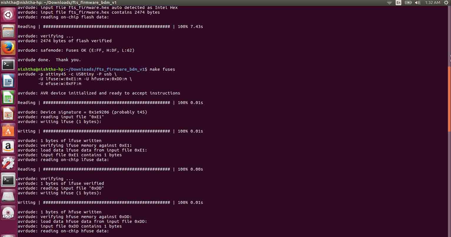
sudo make fuse
Now we'll check to make sure that the USB on your board works, before blowing the fuse that will enable it as a programmer. Unplug your board from the USB port and disconnect the programmer, then plug it back in to the USB.
Make sure the programmer you used to program your board is also disconnected from the computer.
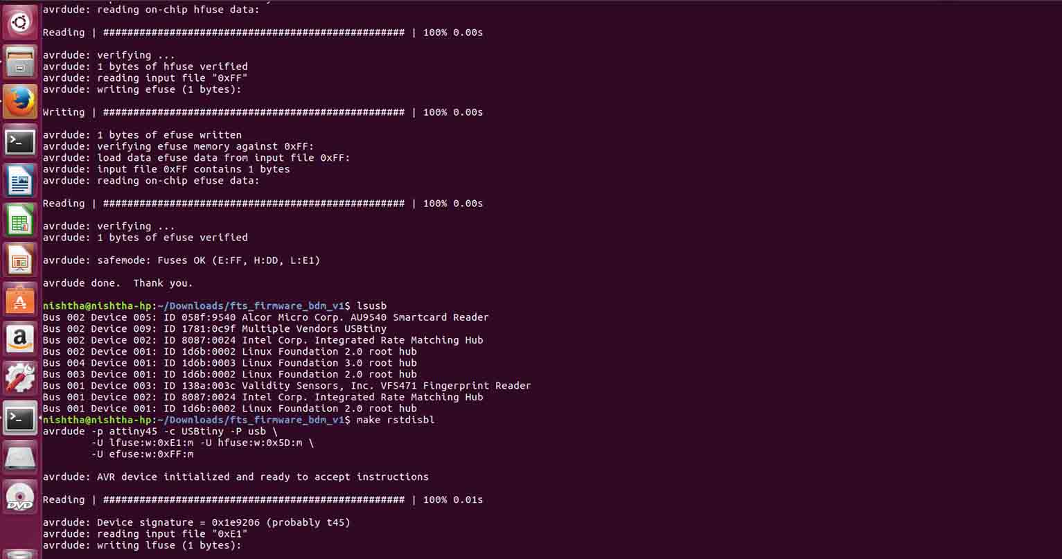
8. Type
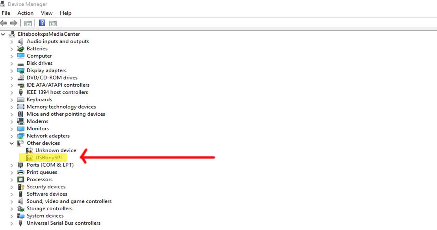
lsusb / which will list USB devices as done in above image
If you see a "Multiple Vendors USBtiny" device, means its working!
9. Congratulations, you're almost to a working programmer. So am I. The ATtiny45 on the board has the code loaded onto it and is working correctly if you've made it this far. There are two final steps left to turn your board into a programmer that can program other boards.
9. Type
make rstdisbl /This does the same thing as the make fuses command, but this time it's going to include that reset disable bit as well. You should see some progress bars, and with that, avrdude will never be able to talk to this chip again through the ISP header.
10. Second, we need to disconnect VCC from the Vprog pin on the ISP header by removing the bridge on the solder jumper. Sometimes the excess solder will stick to a clean soldering iron tip; if not, use desoldering braid to remove the solder from the jumper, thus breaking the connection..
Thats how i secured my FabISP with glue:
Original FabISP files can be downloaded from here BRIAN and DAVID
