
Output devices
To fulfill the assignment I decided to use a modified satsha Kit Satsha Kit originally made by Daniele Ingrassia and modified by me, along with a stepper driver also made by Daniele called Satstep6600 Satstep6600.
Modifying the Satsha Kit
I have already developped a modified Satsha kit that would be perfect for this task I just added one minor modification regarding the routing. Also I am using this assignment as part of the machine building group assignment.
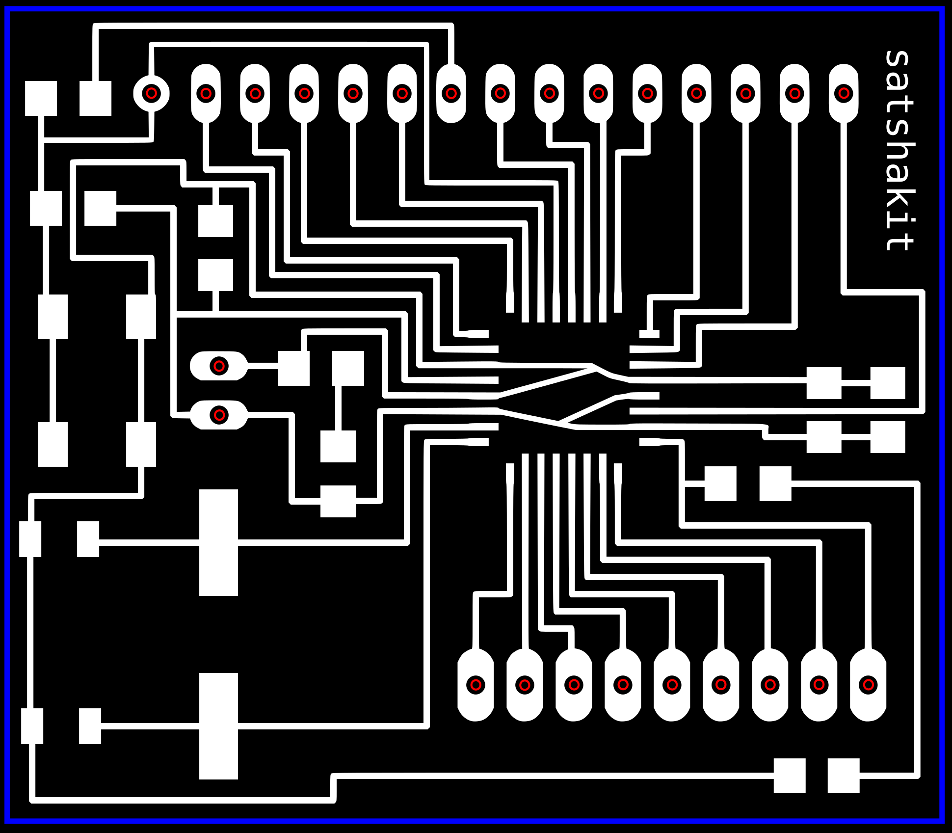
This is how the original SatshaKit looks like
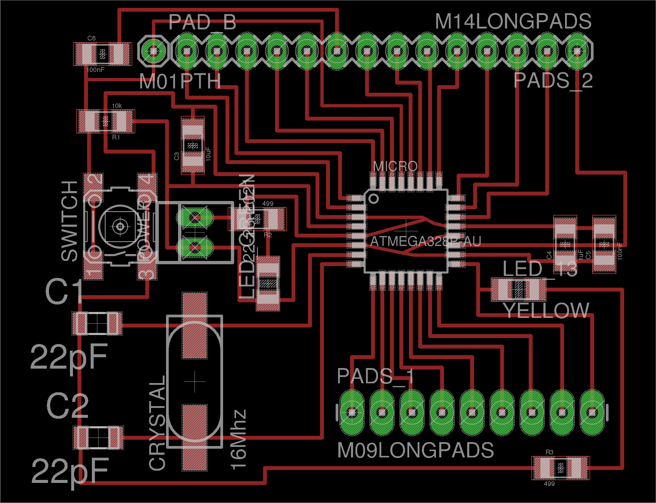
First step was to download the original schematic file and open it to add my modifications. I decided to make four as follows:
-First to add extra pins for I2c to be able to connect more than one sensor to the board .
-Second to add extra pins for Ground, VCC 5volts and 3.3 Volts .
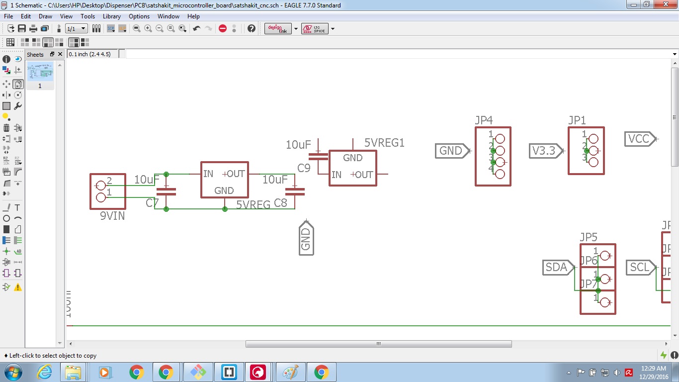
-Third to add a 3.3v regulator circuit to be able to take 3.3v from the board.
-Fourth to add a 5v regulator to be able to connect the board directly to a 9v battery.
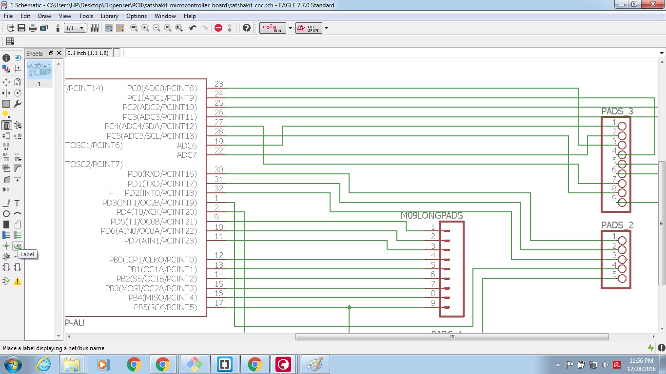
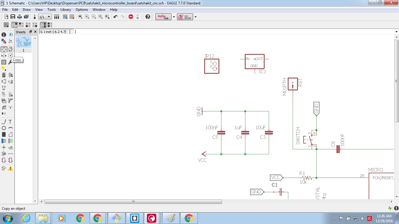
First Modification:
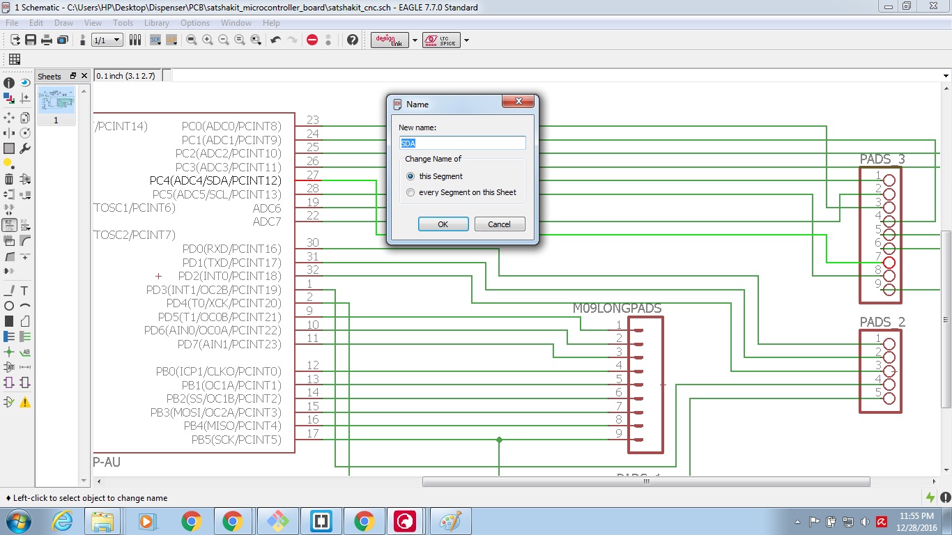
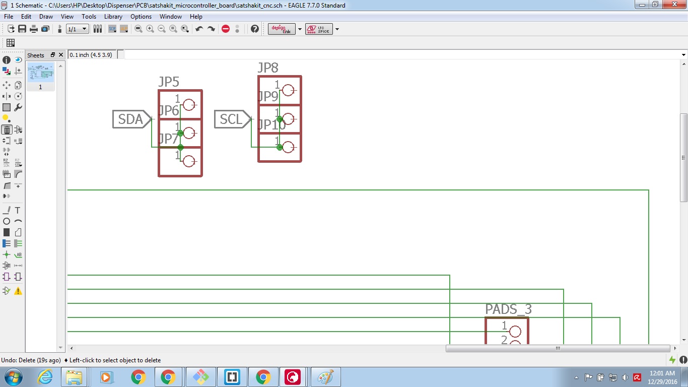
Right click the wire connected to pin 27 of the IC and click on name.
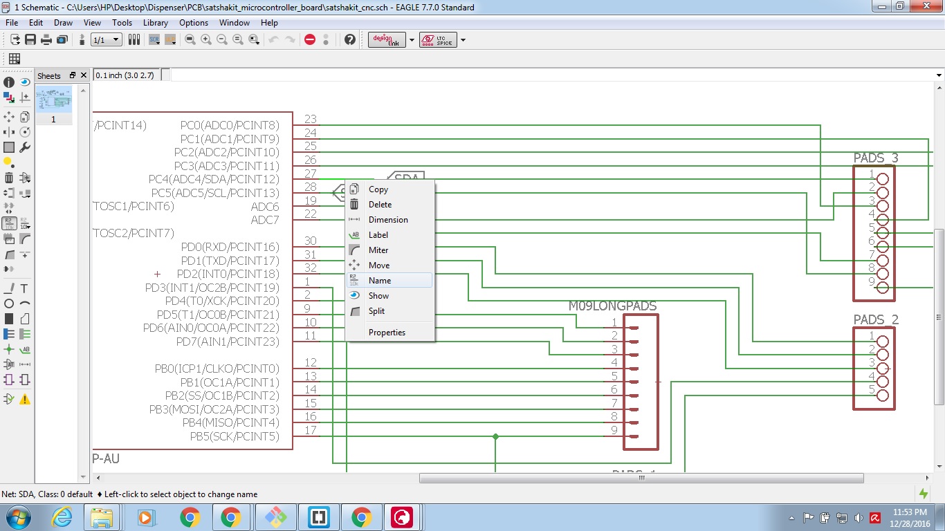
Type SDA and click OK.
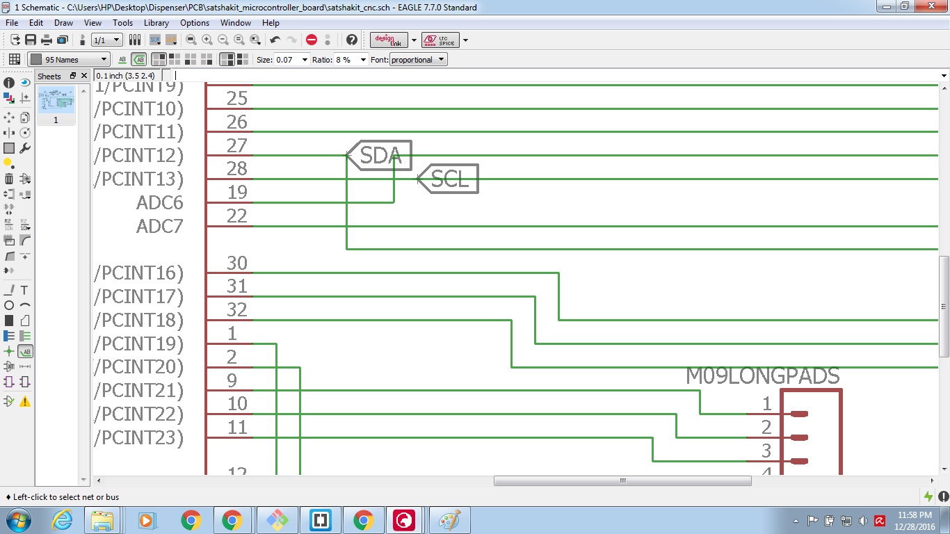
To add a label to the wire with its name Click on Label-->check bottom left corner of the image.
I like to use the Xref -->check upper left corner of the image.

Click on the same wire you named SDA, This is how it should look.

Do the same for the other pin of the IC naming it SCL.
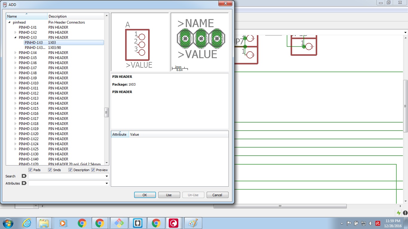
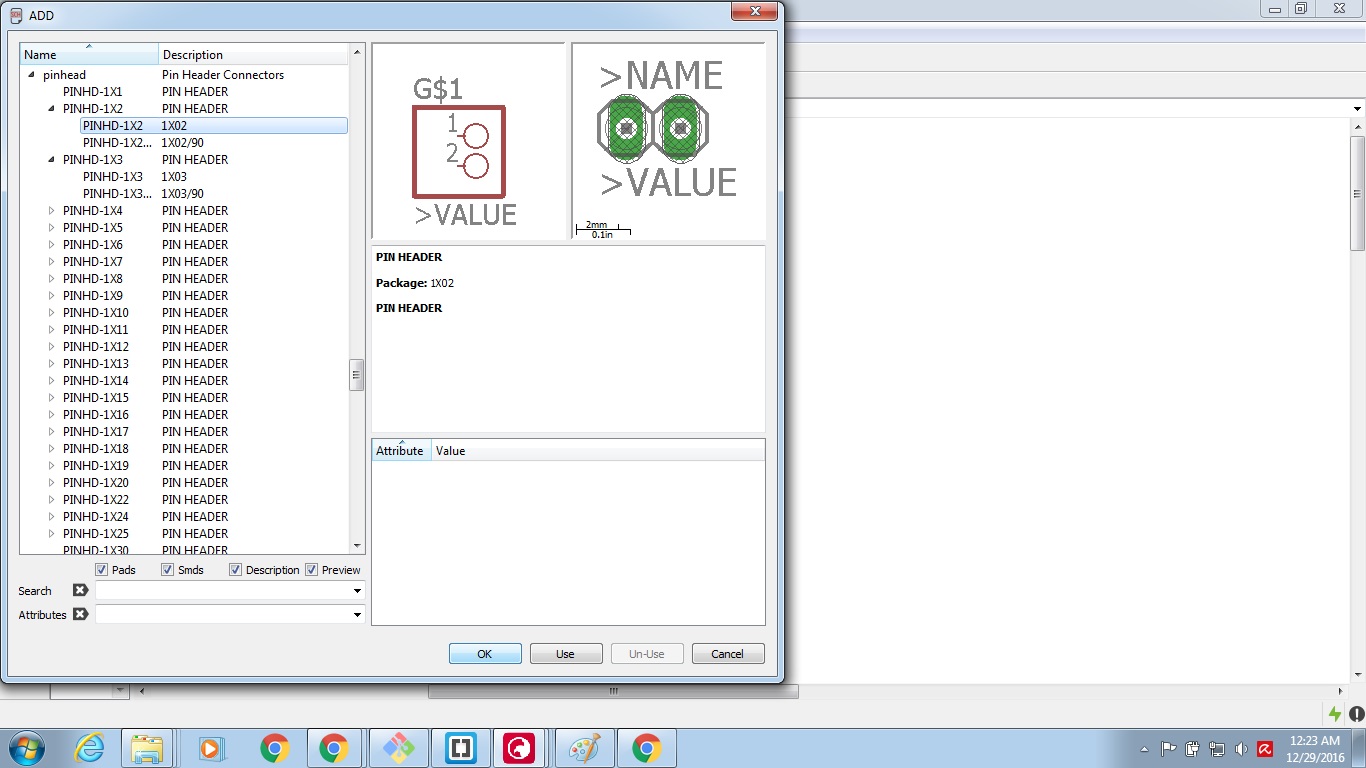
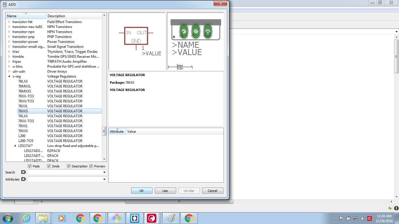
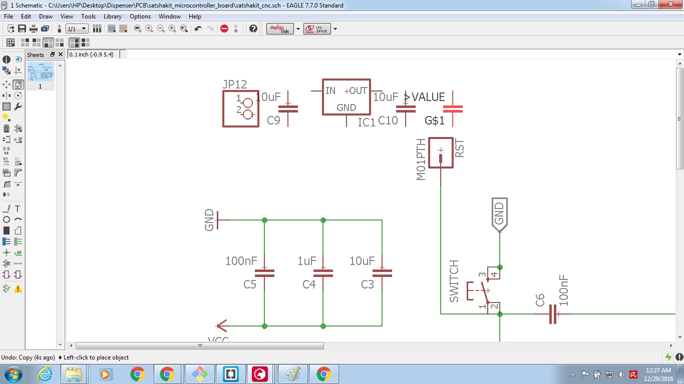
Now add the extra pins, Click on add button -->check upper left corner of the image.
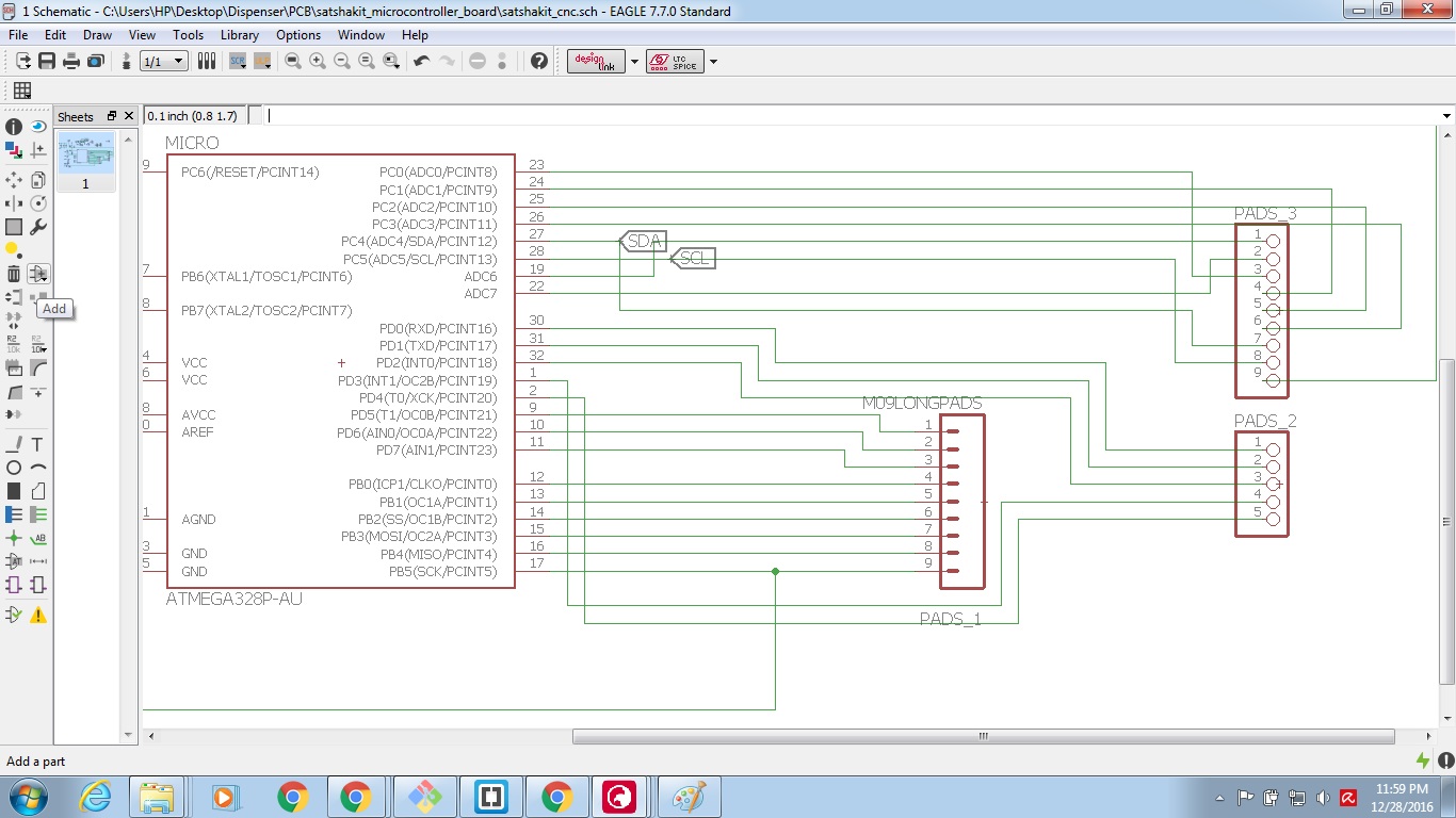
Scroll down to Pinhead. And since I chose to add 3 extra I chose the third one and then the first one. Then press OK.
Click in the place you want add the part, Add 2 of these. And then click on Net -->check lower left corner of the image.
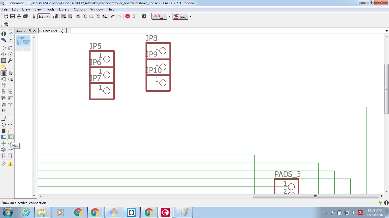
Connect the pins as shown and then name the wires and add labels same as before.
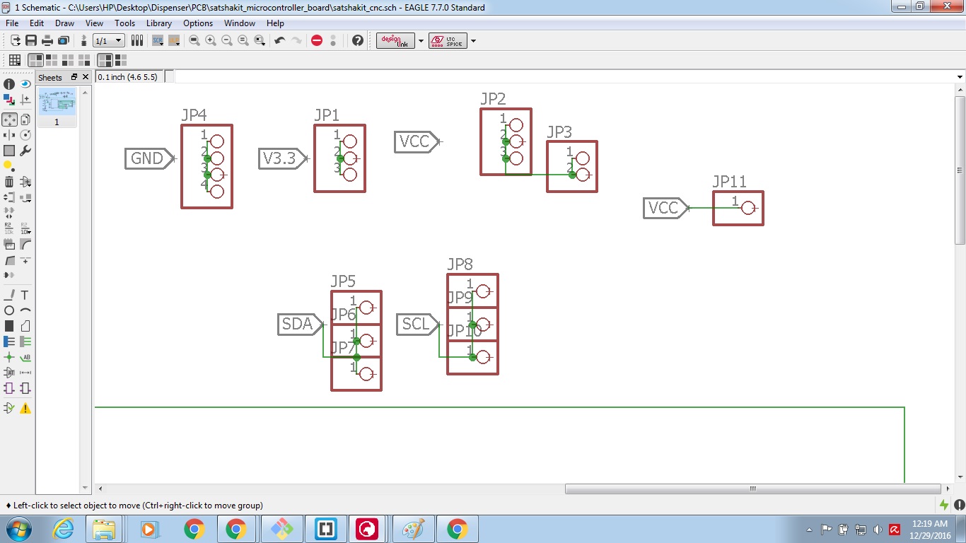
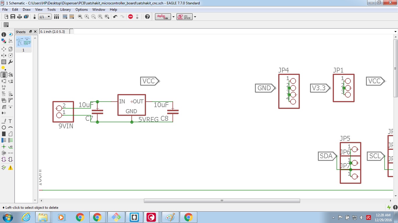
Second Modification:
Add some pin header groups for VCC, Ground and 3.3V using the ADD button. Connect them using Net button, name them and add the labels as shown.
Third Modification:
We need to add pin headres to connect the battery, voltage regulator and capacitors.
First place the pinheaders .
Scroll to find vreg and choose the one shown in the picture.
As we need to add 10uF capacitors the easiest way would be to copy the one we need from the design.
Click on the copy icon and use it to copy the part you want -->check upper left corner of the image.
Add them as shown.
Connect them using Net button as shown.
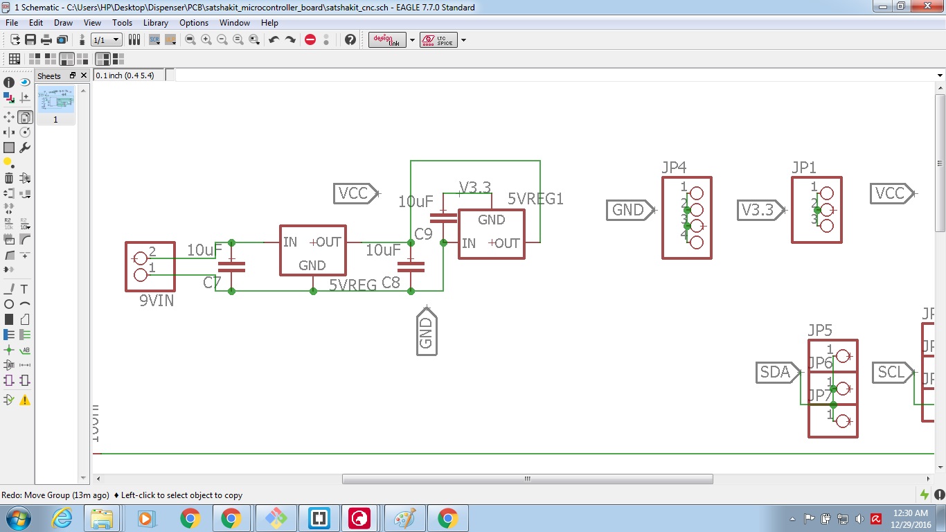
Fourth Modification:
Add another Vreg and a capacitor as before.
Connect them as shown. The reason the connection is like this is because I used the same Vreg as in modification three although the Pinout of the 3.3Vreg is not the same as the 5V but I couldn't find it in eagle.
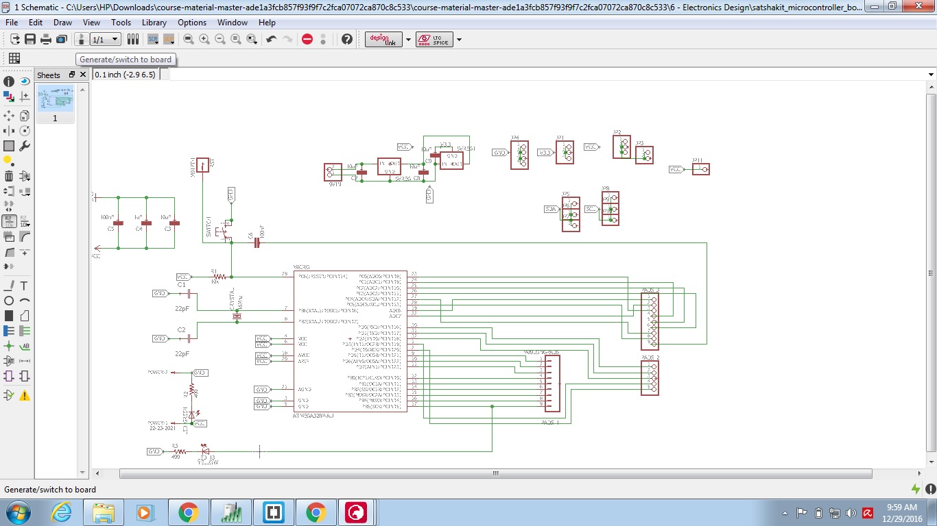
Time to edit the Board file .
Click on switch to board button .
My Idea was to free some space in the lower left corner of the board.
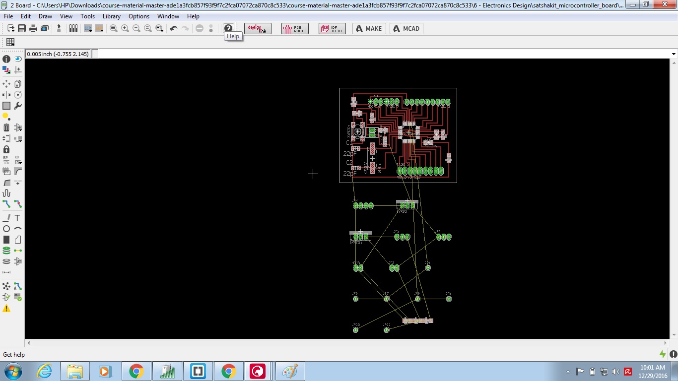
Click on Ripup and remove all wires connecting the crystal and then right click on it and move it to the right.

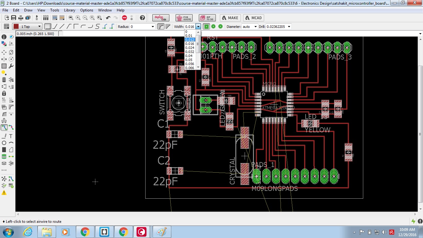
Now connect the wires back using the Route button next to Ripup.
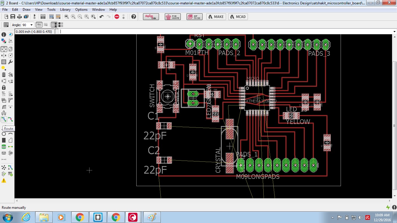
Use the width of 0.012 and make sure you are on the top layer all the wires should be red.
Now We have the place we wanted.
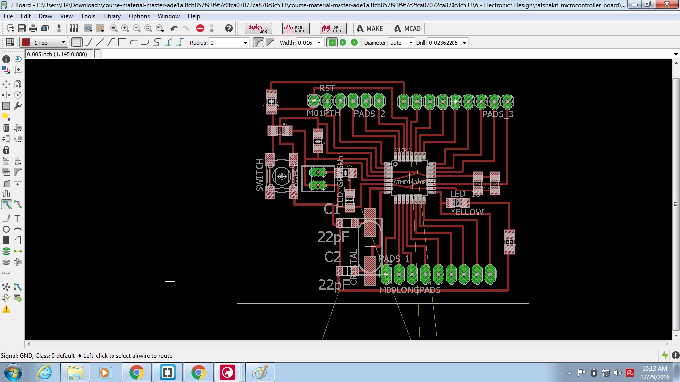
Using the same commands Move, Route and Ripup try to arrange all the components in the area.
Final modification was to reroute the traces going under the IC.
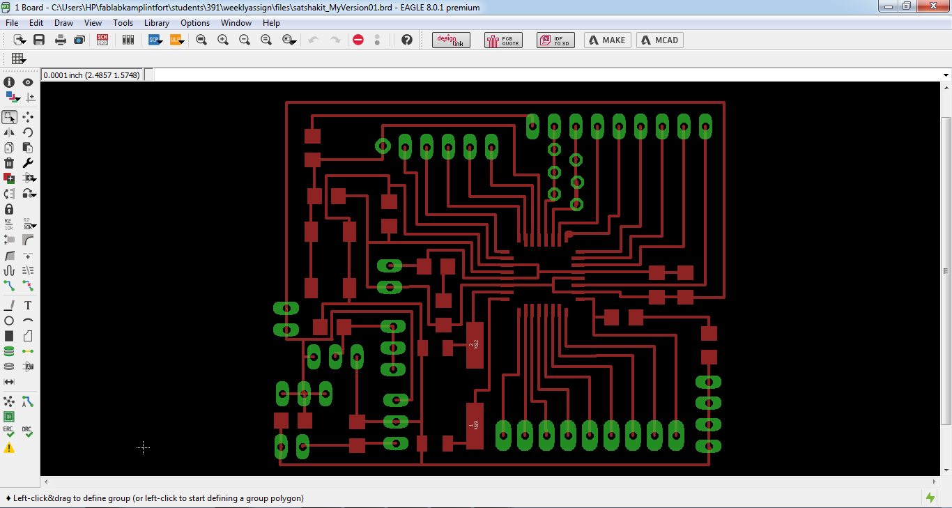
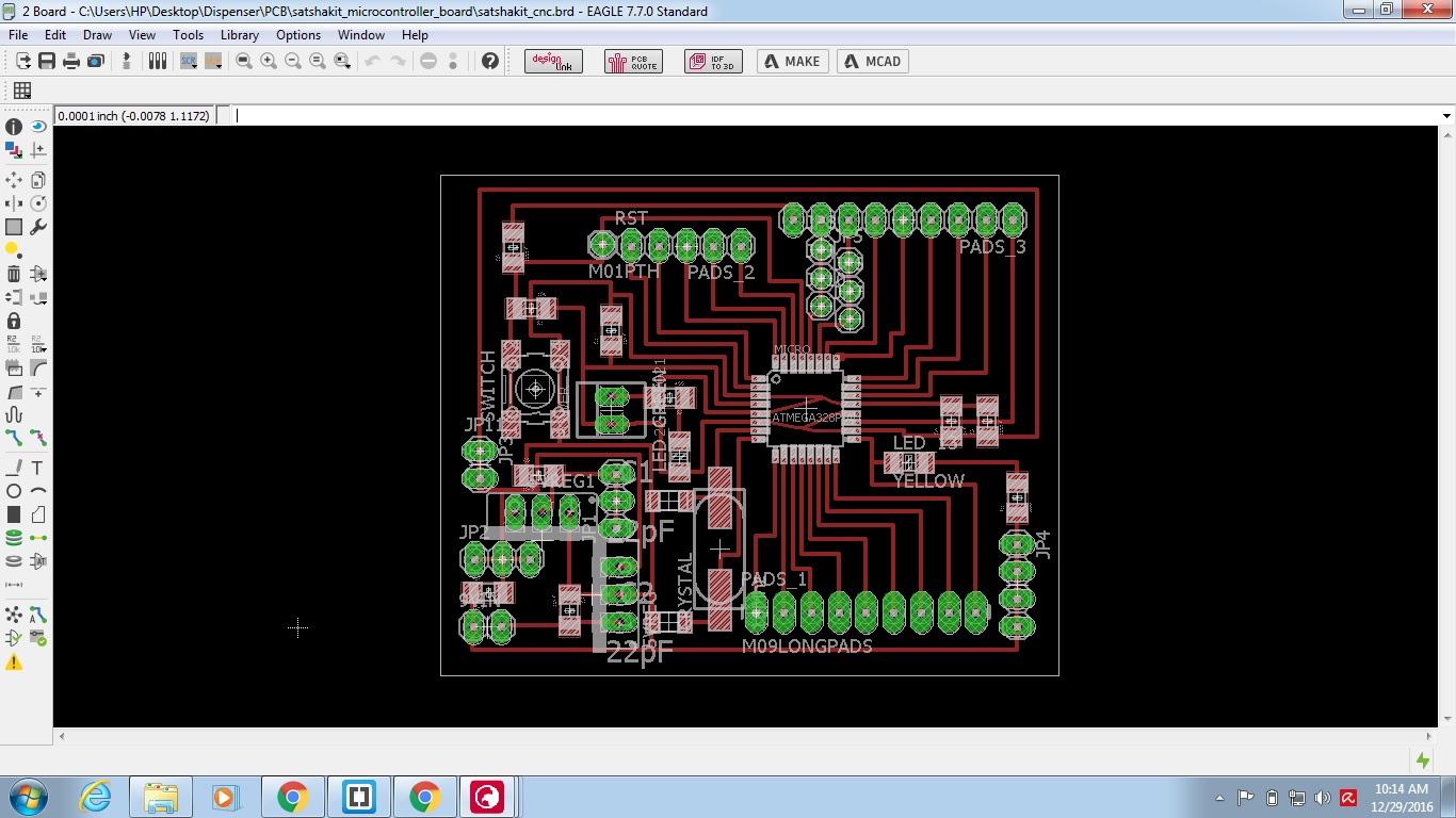
Finally I exported the design as shown above.
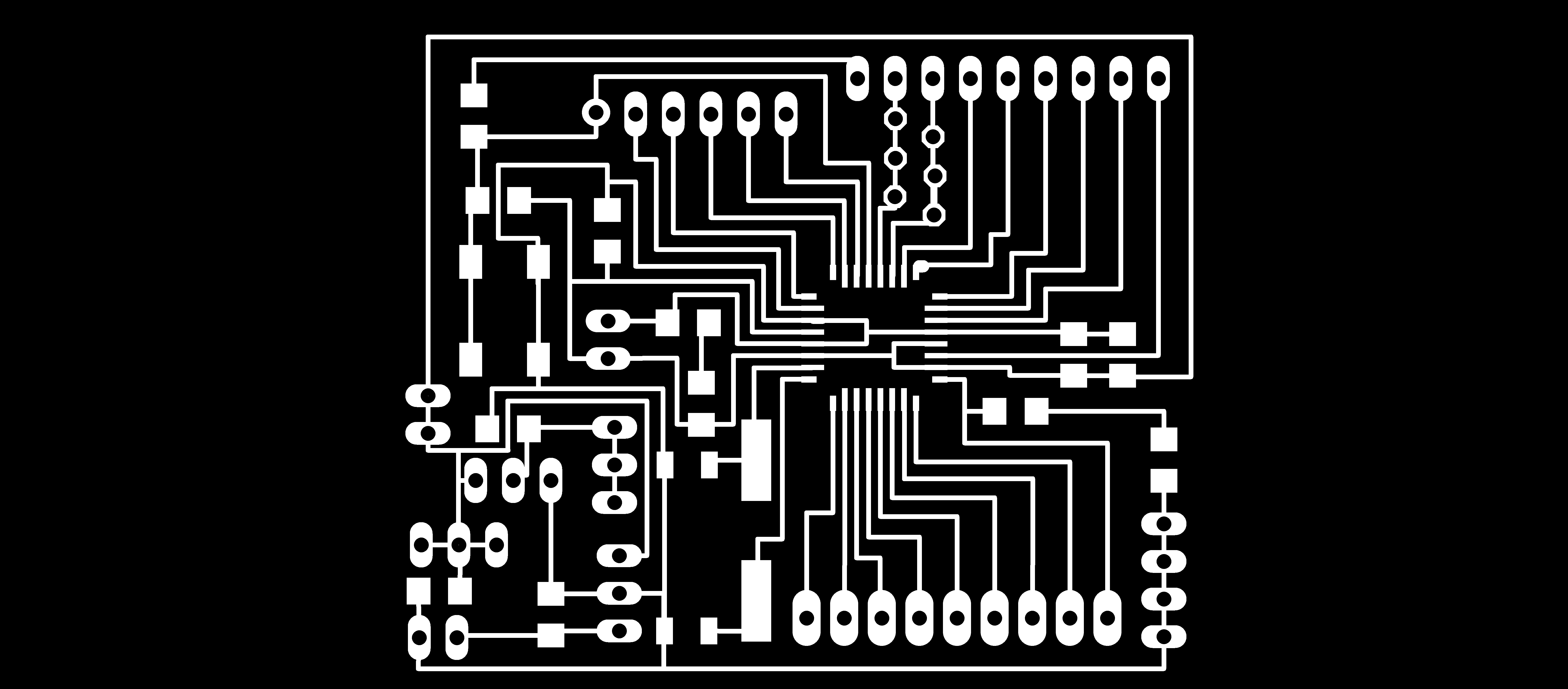
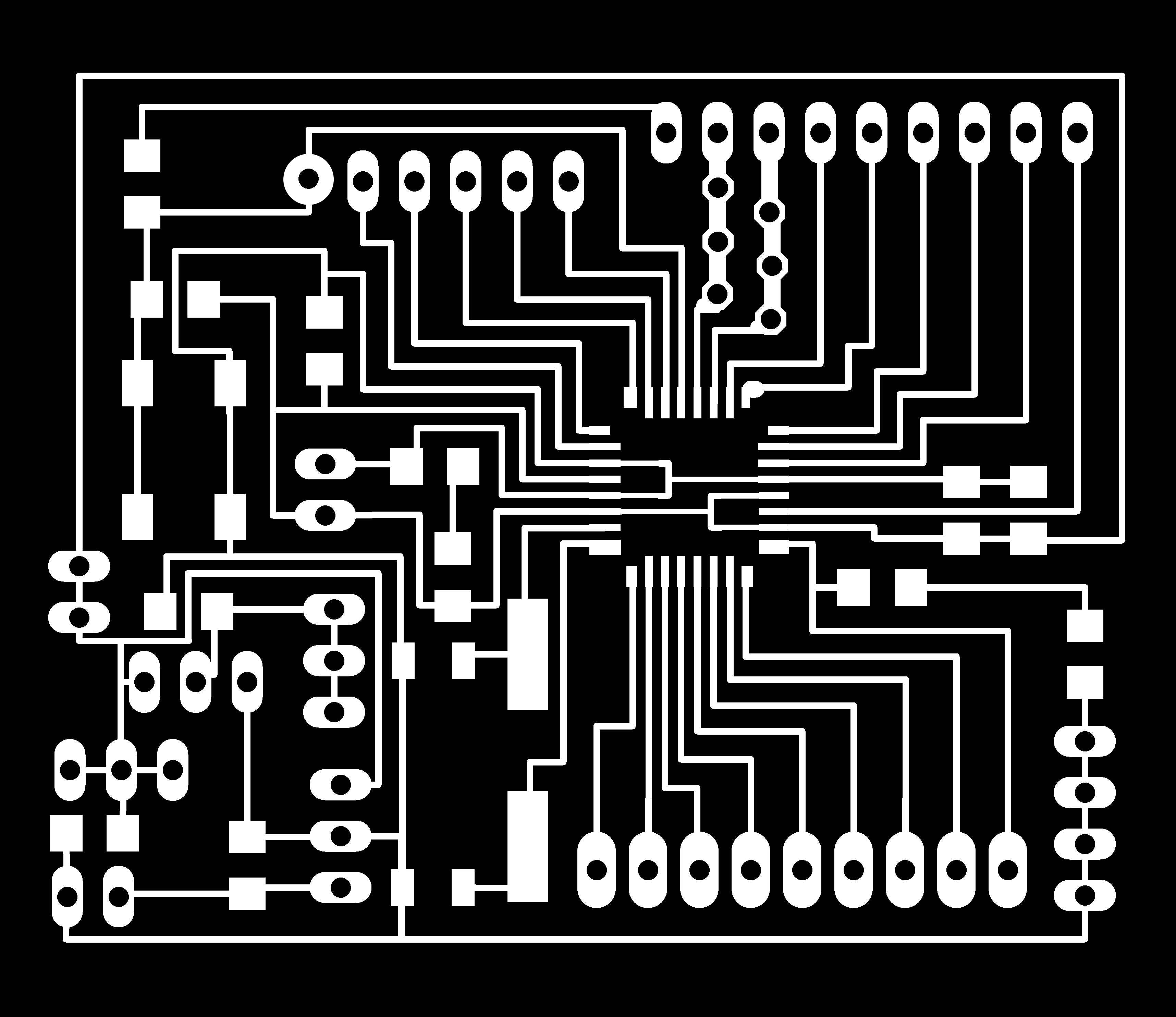
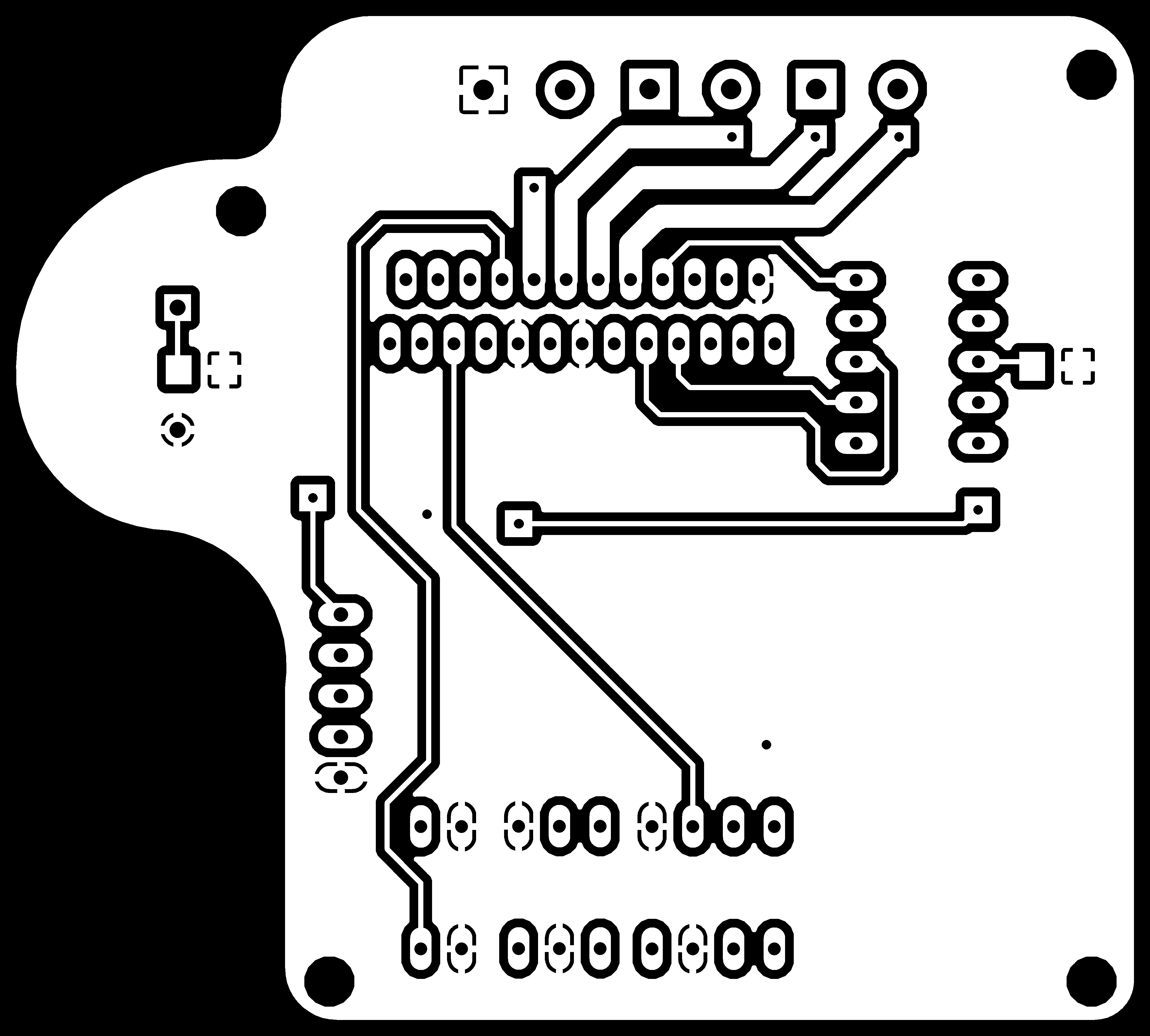
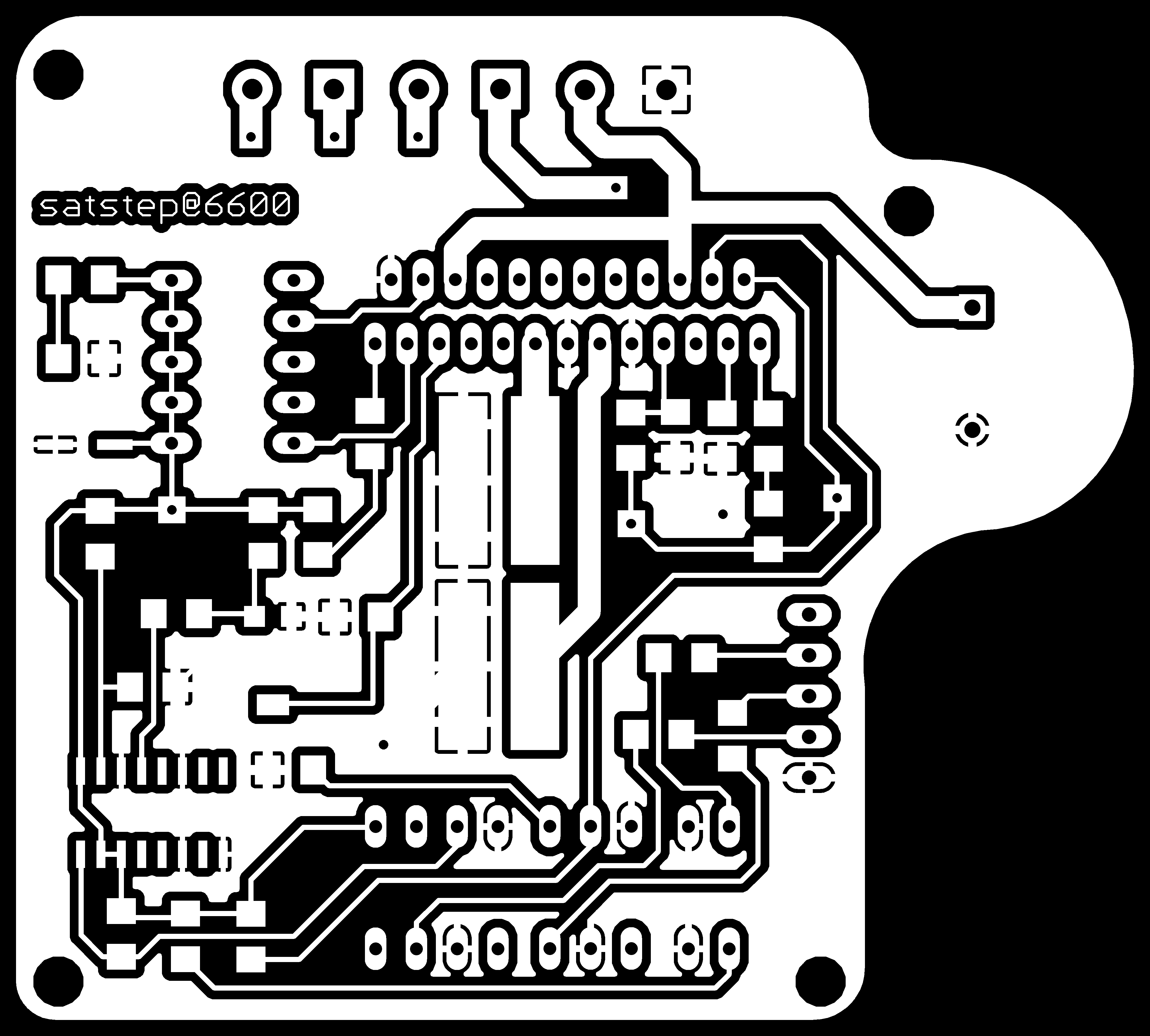
Here are the 2 images to be used for the CNC machine.

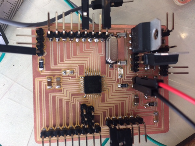
Making the stepper controller
I followed Daniele's repository to fabricate the board here are the images I used for milling


Here are the settings:
Machine: MDX-40
Speed: 4
Send Command: mod_lp.py/dev/usb/lp0
Server: Localhost:12345 In my case Local host was 127.0.0.1
Cut depth: 0
Tool diameter: 0.2mm
Number of offsets: 4
Offsets Overlap: 55
Programming
Then I uploaded the GBRL firmware to my board
Finally I used Universal G code sender to move the motor just to test everything.
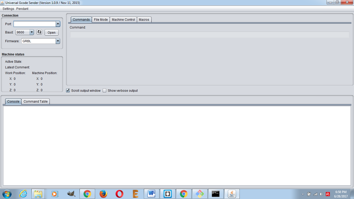
Here are some of the G-code examples I sent using the G-code sender:
G0 X0 --> to move x axis to zero position
G0 X50 --> to move x axis 50
G0 X0 Y50 --> to move x axis to zero position and y to 50
G1 F3000 --> to set the feedrate to 3000
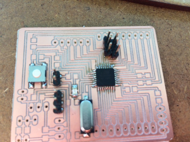
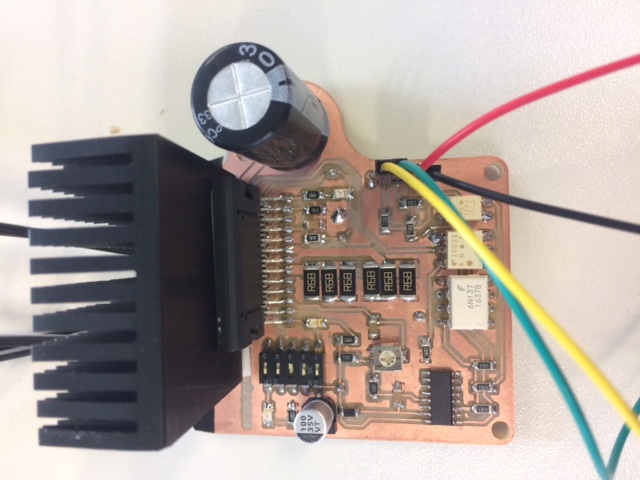
Final product
Downloads
-Schematic-Board