Electronics design
Week 6
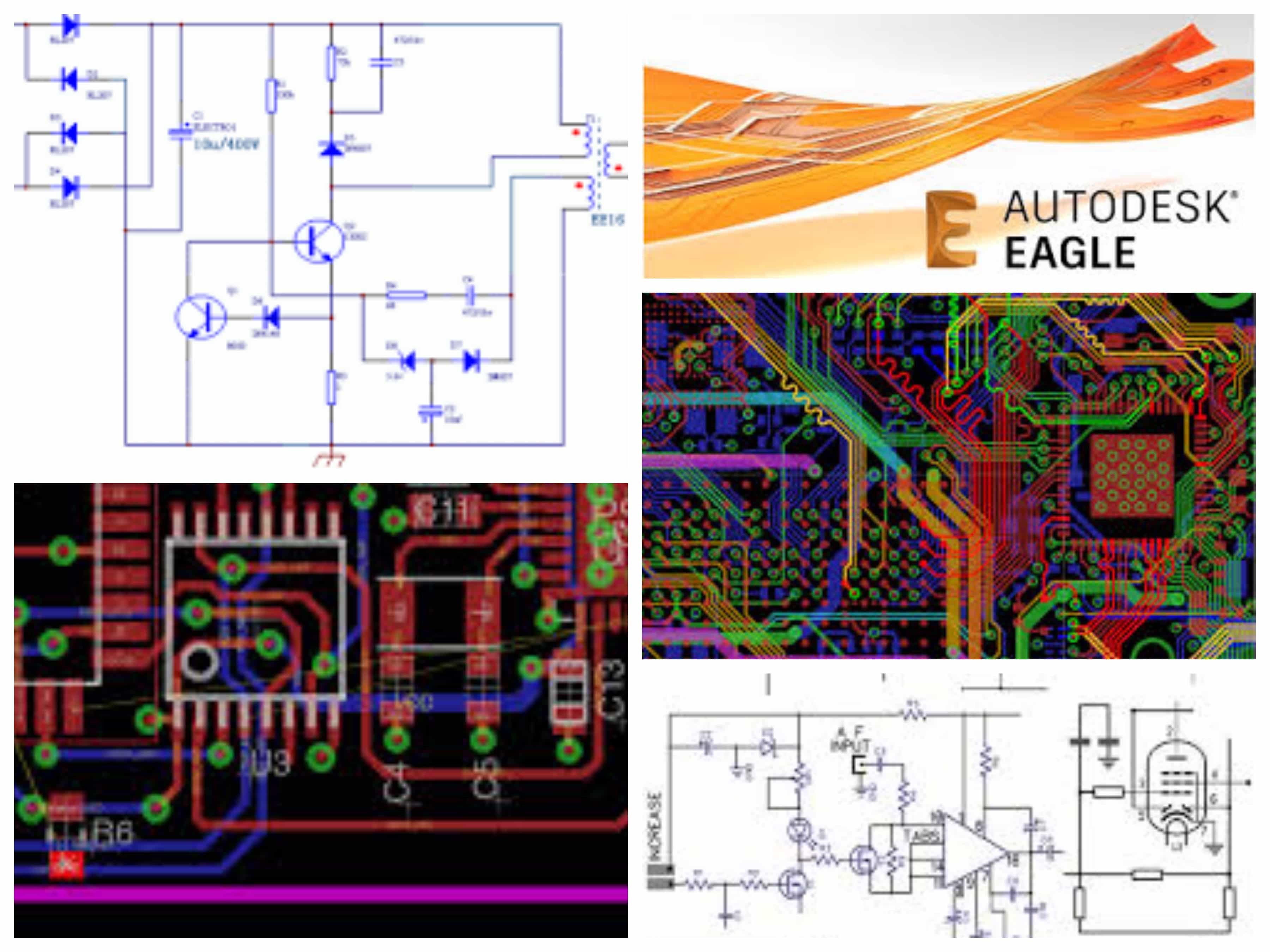
Discovering Eagle and basic electronics
I've never used any kind of software like this one before or do
any electronics work at all. So, this week was pretty new for me.
Well, I've never designed any circuits before too. I thought it was
pretty interesting but I definitely needed a little introduction to
many concepts and the software to although the Fab Academy tutorial
was already really complete. I looked at a lot of tutorials as you
can see in the left section. Passing from electronics basics to
eagle itself. After those tutorials, added to the Fab Academy
tutorial, I've been able to design my first PCB. I thought I
was a very interesting week because I'll have to design some
circuit for my final project, as for all of us I guess. Now, I'm
completely sold to it! I love that software.
Designing the PCB
To begin with, as the Fab Academy tutorial is already very complete, I'm not going to detail all the steps I followed to design that PCB because well, they're the same than in the tutorial. I have to say that I didn't any major difficulties to do that part of the assignment. The only thing you have to do is read well the steps and follow them as precisely as you can. This is what I did so, it went well. Still, I would like to underline some of the steps I found the most important or the interesting to me.
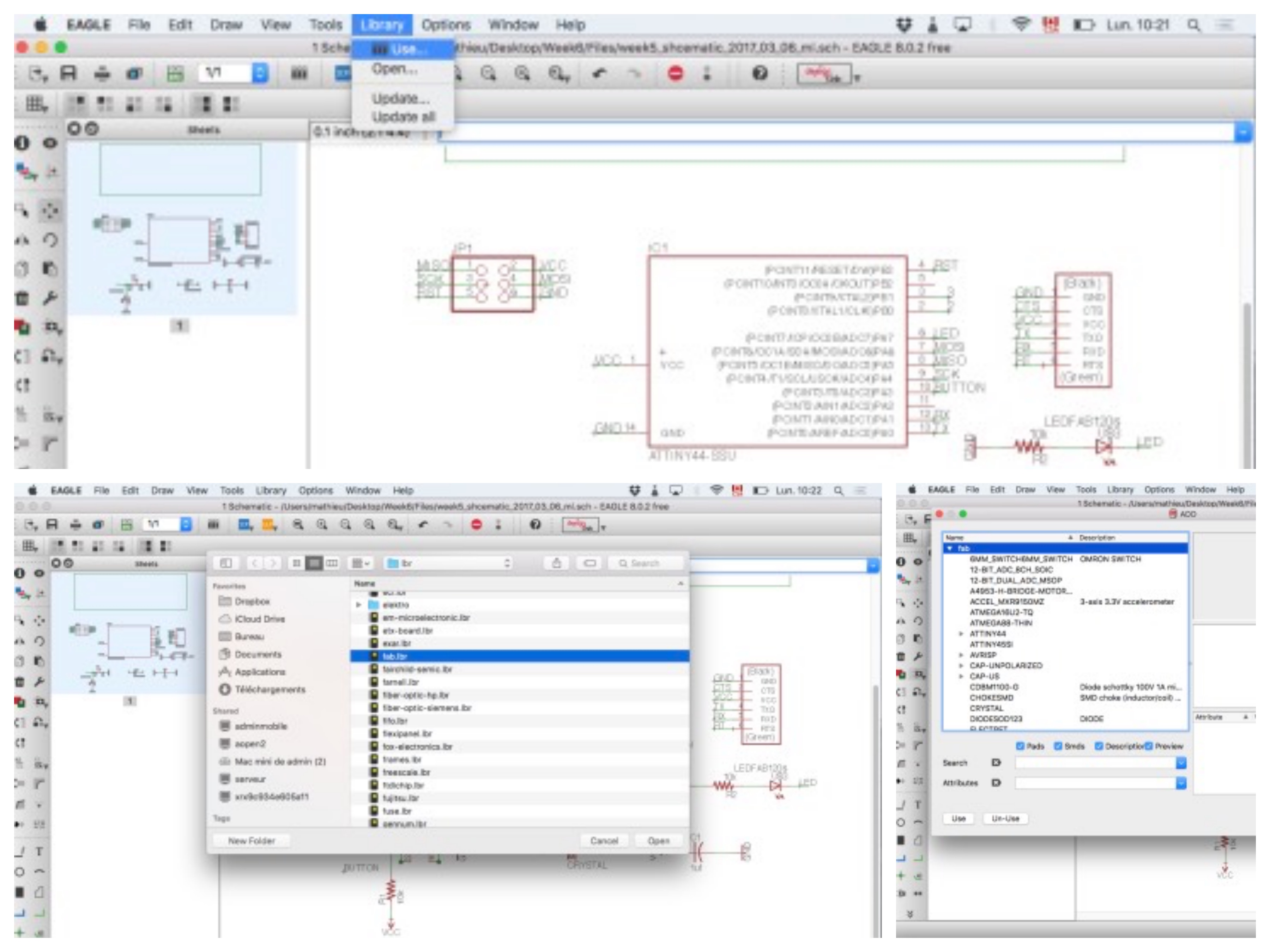
1.Importing the parts libraries
This was a very important step because you have to find the right component to put on your PBC. There were some major libraries that were needed to be added so you'll have all the component needed for this assignment.
Fisrt, the Fab librarie :
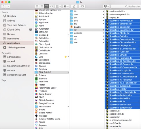
Then, the sparkfun batch of libraries (That I thought I needed but finally I didn't) :
To be able to use them, you have to tell the software to do so and then you'll see the choices in your add menu.
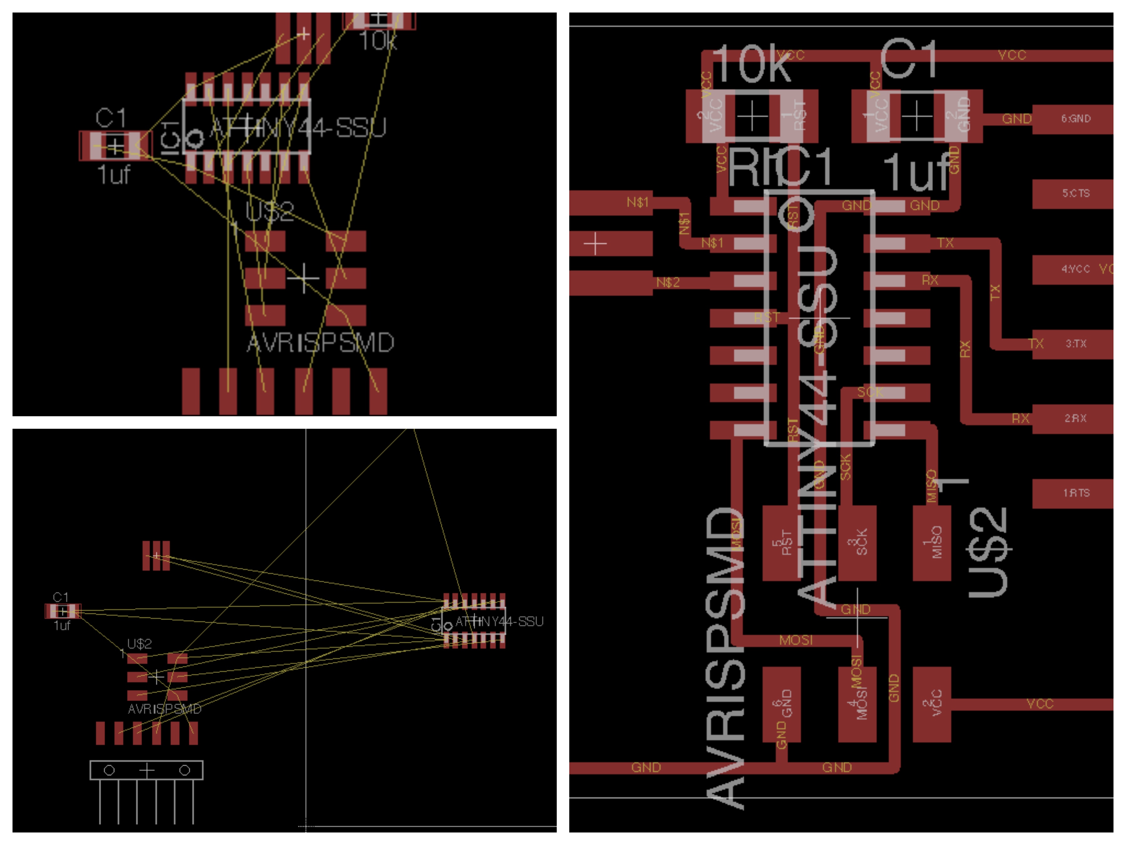
2.Importing the parts
Here's a list of the components needed :
Then, you press the add button and go to the right libraries
to find the components that you need. There's no need to place
them right away at a good place, you'll do it in the next steps.
This said it seemed good to me to already visualize a little bit
how the PBC will look like. Also, just to make it clear, because
it took me a little while to understand that, you have to press
on the little + symbol to access the part and move/rotated them  .
.
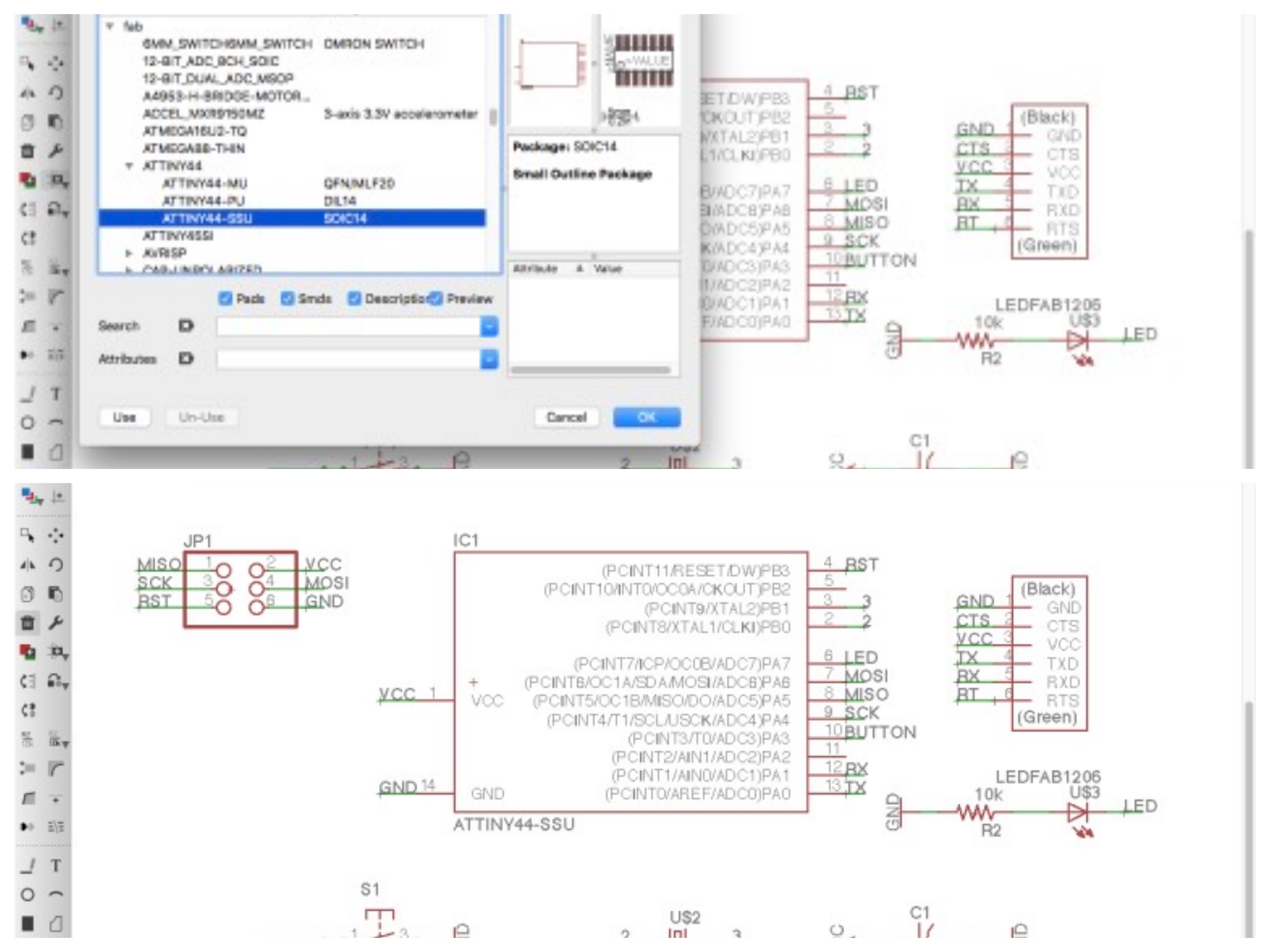
This was the last part of the schematic phase.
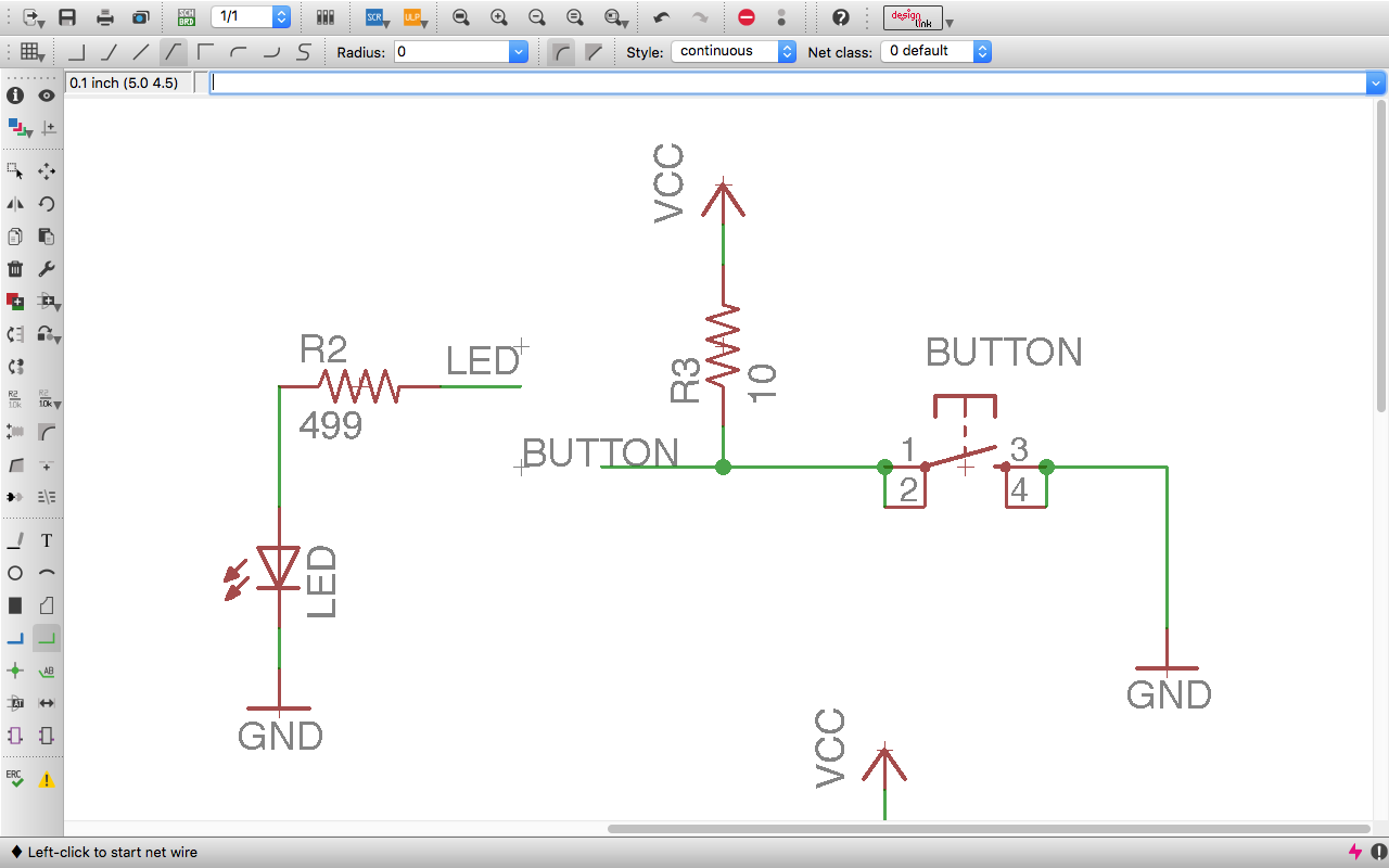
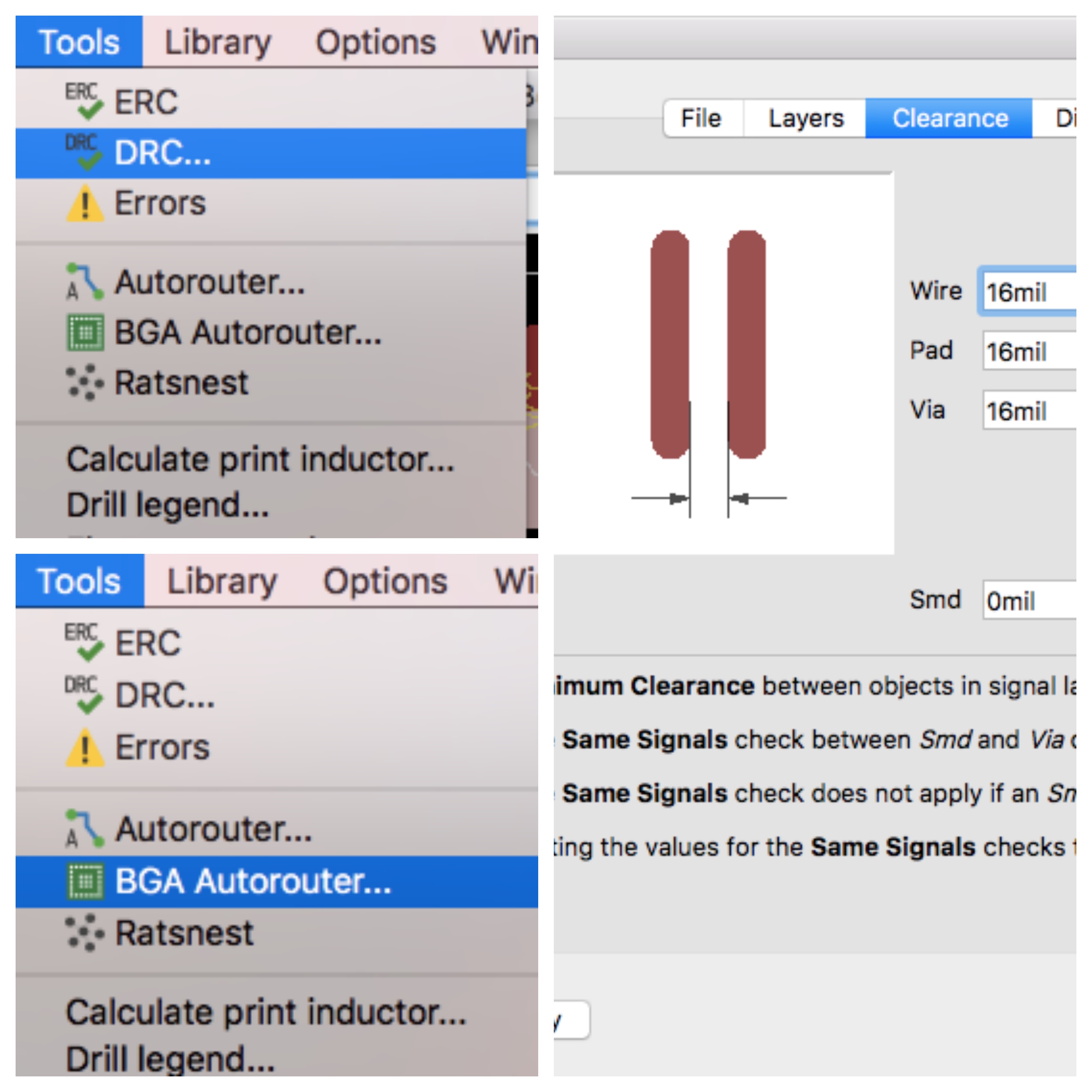
3. Preparing the board
Now that I have a schematic, I passed to the board section pressing
that button  .
Then, the screen changes and the prints of the parts appear with the connection
that they need. In this case, I placed then as the FabAcademy tutorials
showed as an inspiration. After this, I gave some design rules to the
software basically to make sure that the paths were wide enough.
Finally, I pressed BGA Autorouter and Eagle gives you options
of paths also giving the percentage of the connection made.
.
Then, the screen changes and the prints of the parts appear with the connection
that they need. In this case, I placed then as the FabAcademy tutorials
showed as an inspiration. After this, I gave some design rules to the
software basically to make sure that the paths were wide enough.
Finally, I pressed BGA Autorouter and Eagle gives you options
of paths also giving the percentage of the connection made.
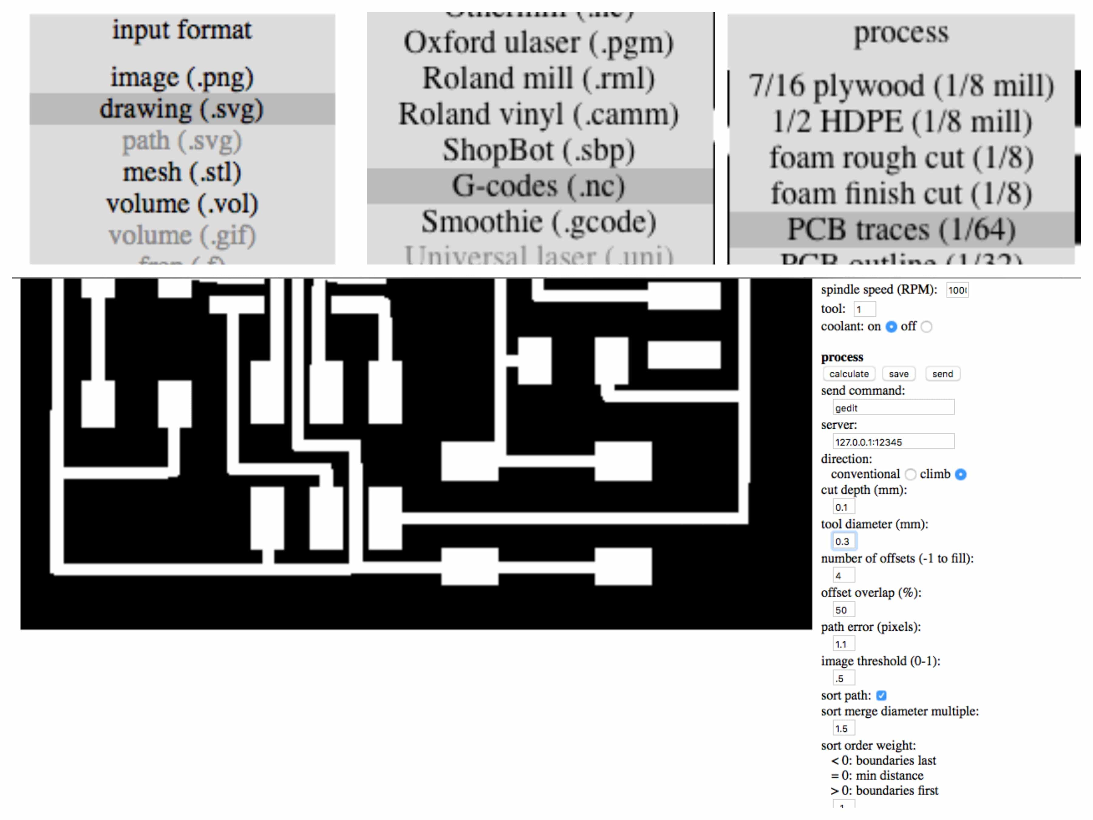
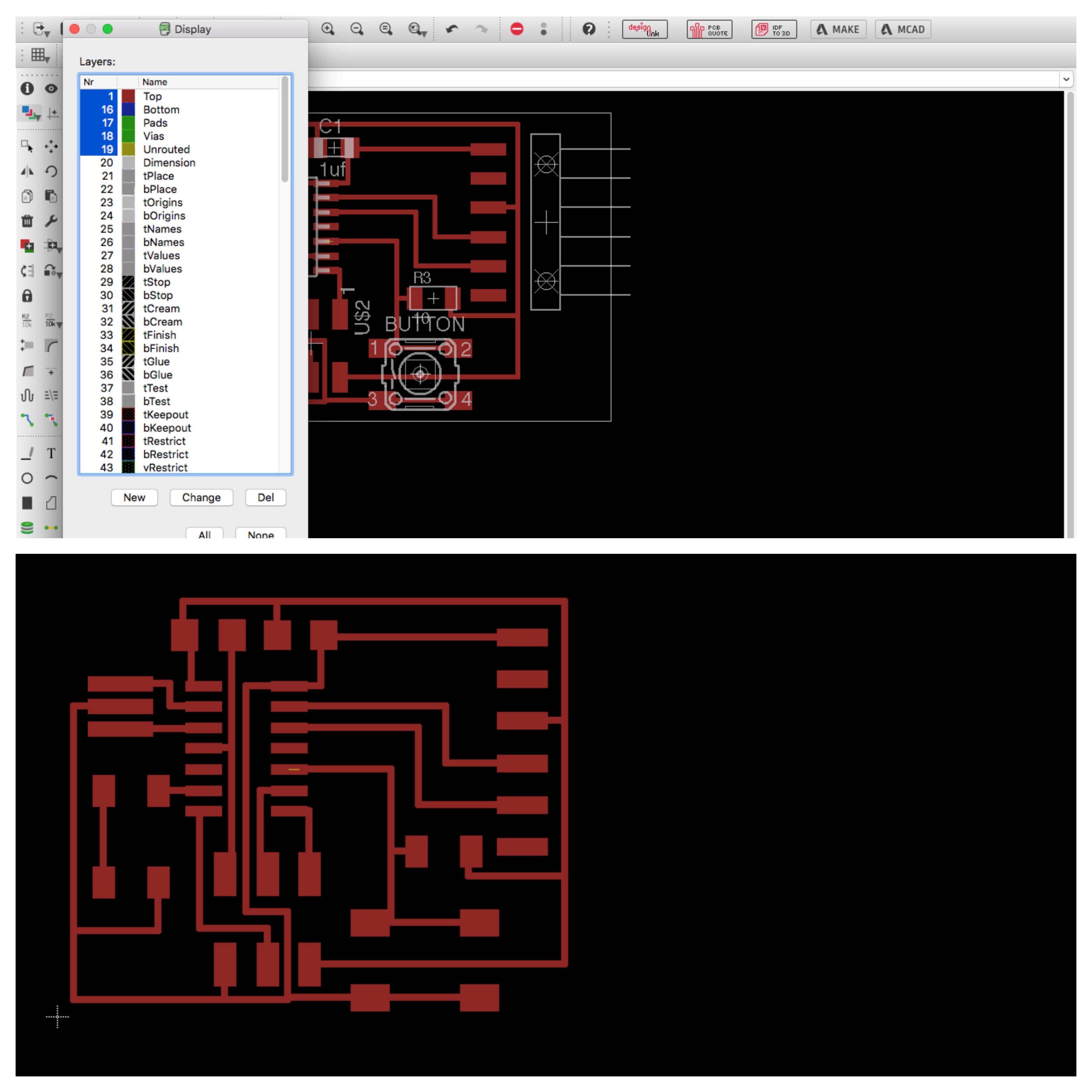
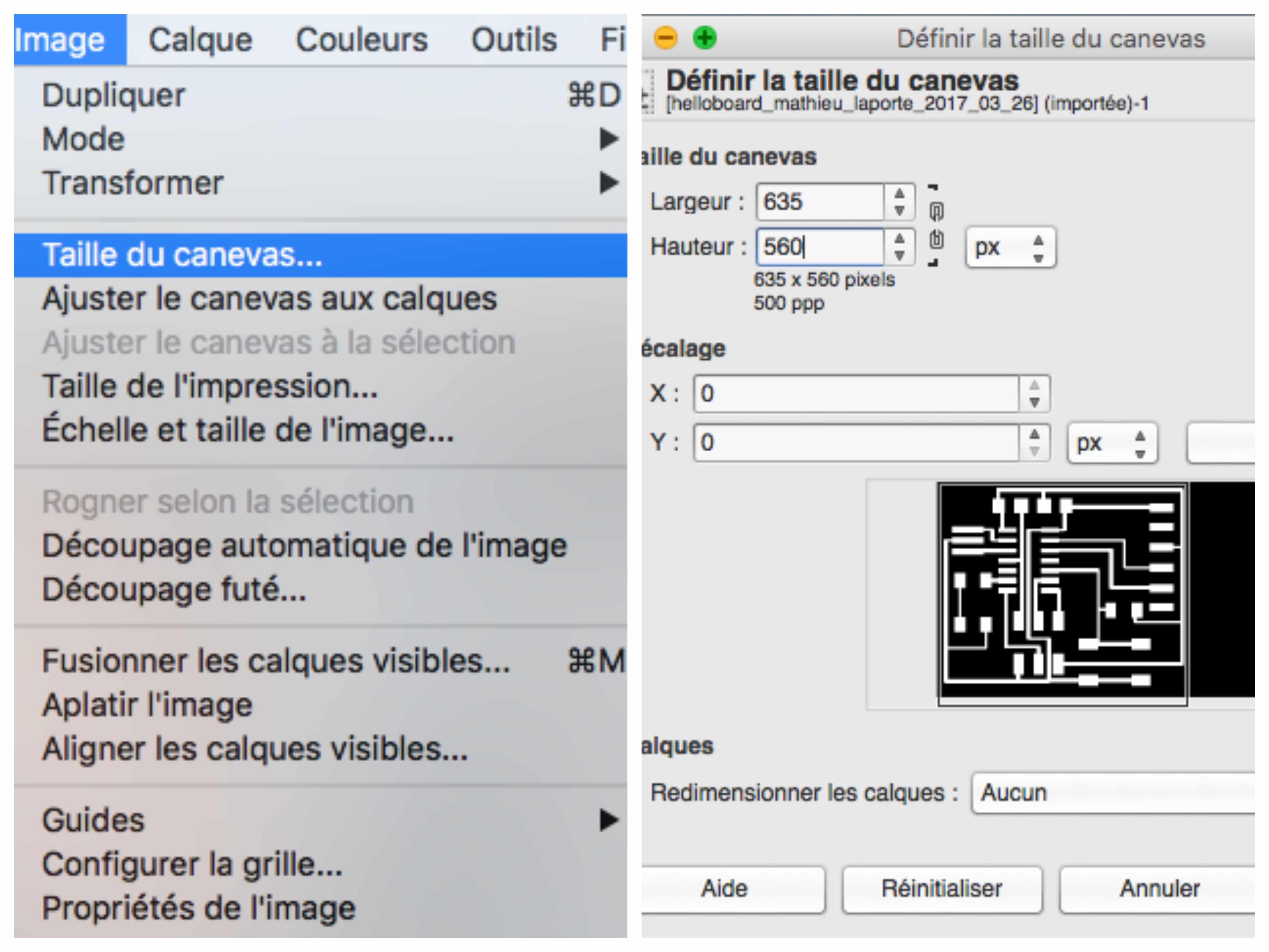
After this, I had to prepare the board to get exported. For that, I had to clean the information showed on the board keeping only the cases 1, 16, 17, 18, 19.
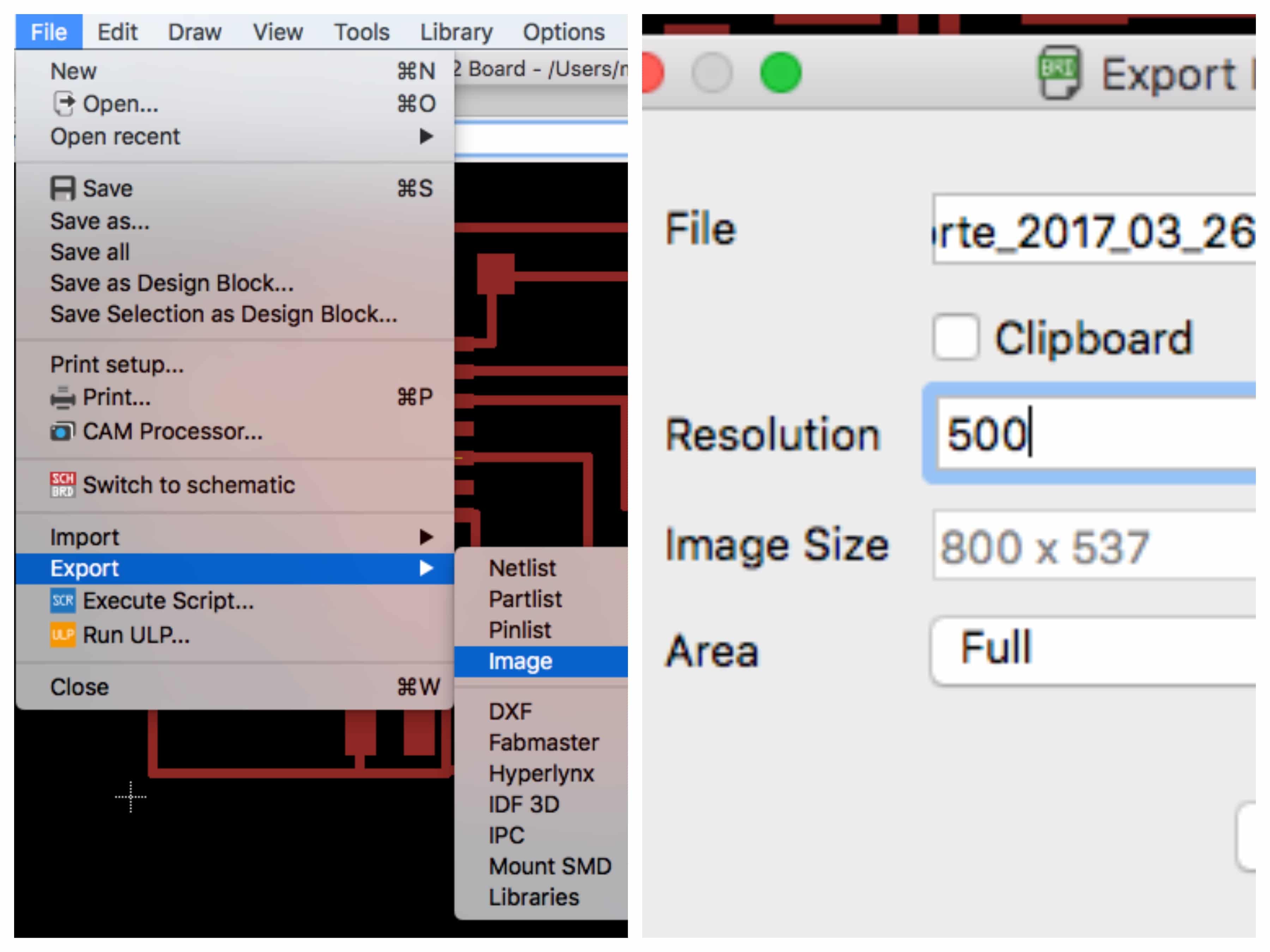
The next step is to export the board as an image (.png). I had to be carefull to put a high resolution because if it's not high enough the FabModule won't read it.
The rest of the job will be on other software, on Gimp, and
on the Fab Modules as well. On Gimp, import the .png and then,
cute the extra parts. Then, I opened it with Inkscape, vectorized
it and saved it in .svg. I prefer to use a .svg file more than a .png
because the clarity and quality on the file will be much better. It
happened to me that the resolution wasn't hight enough in .pgn and
the FabModules couldn't read it well. A .svg file will do the job very well.
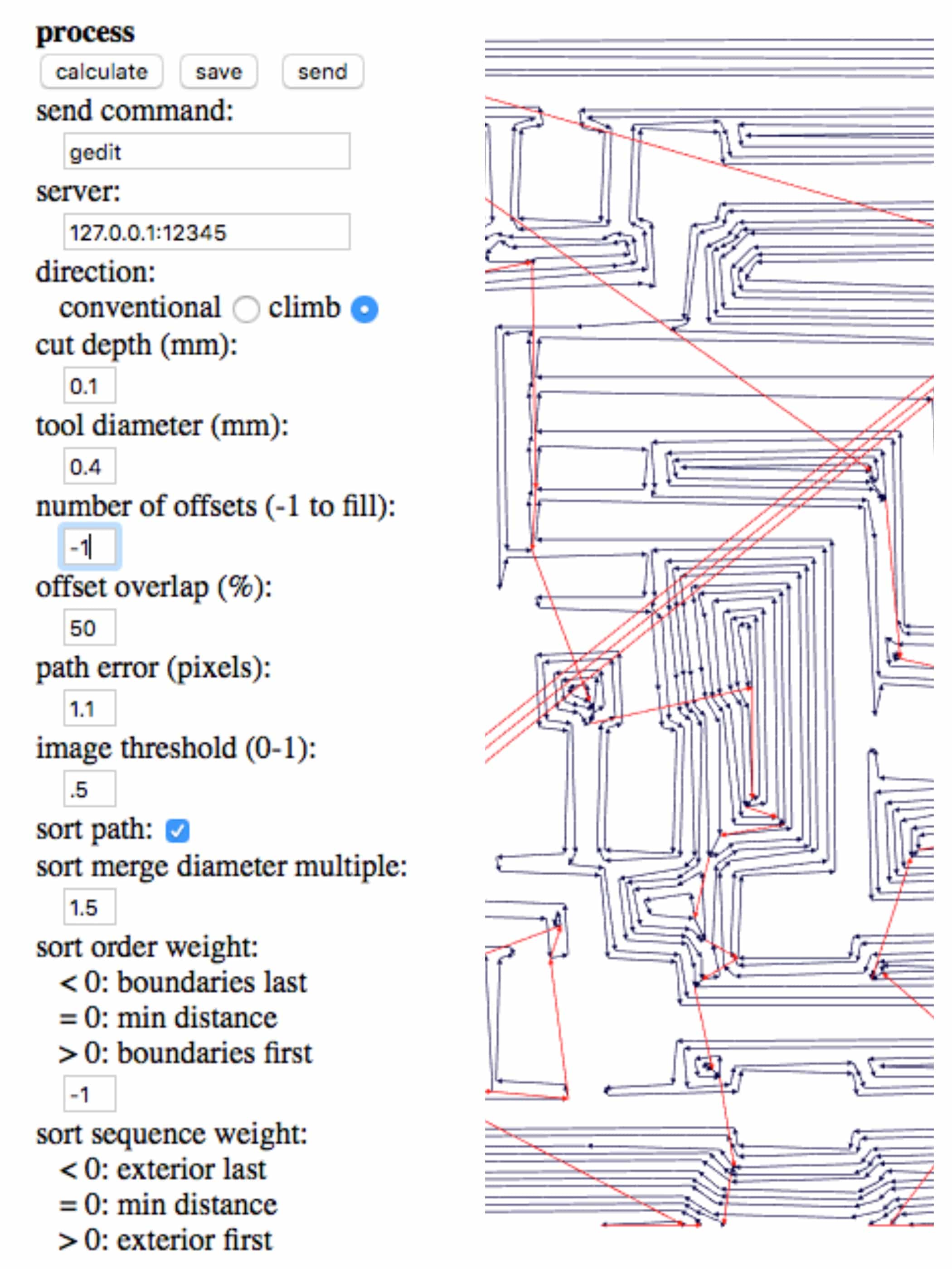
Finaly, I prepared the board for the milling with Fab Modules.
Then, I milled it. I'm not going to document more on this suject
because it's the same than in the Electronics production week.
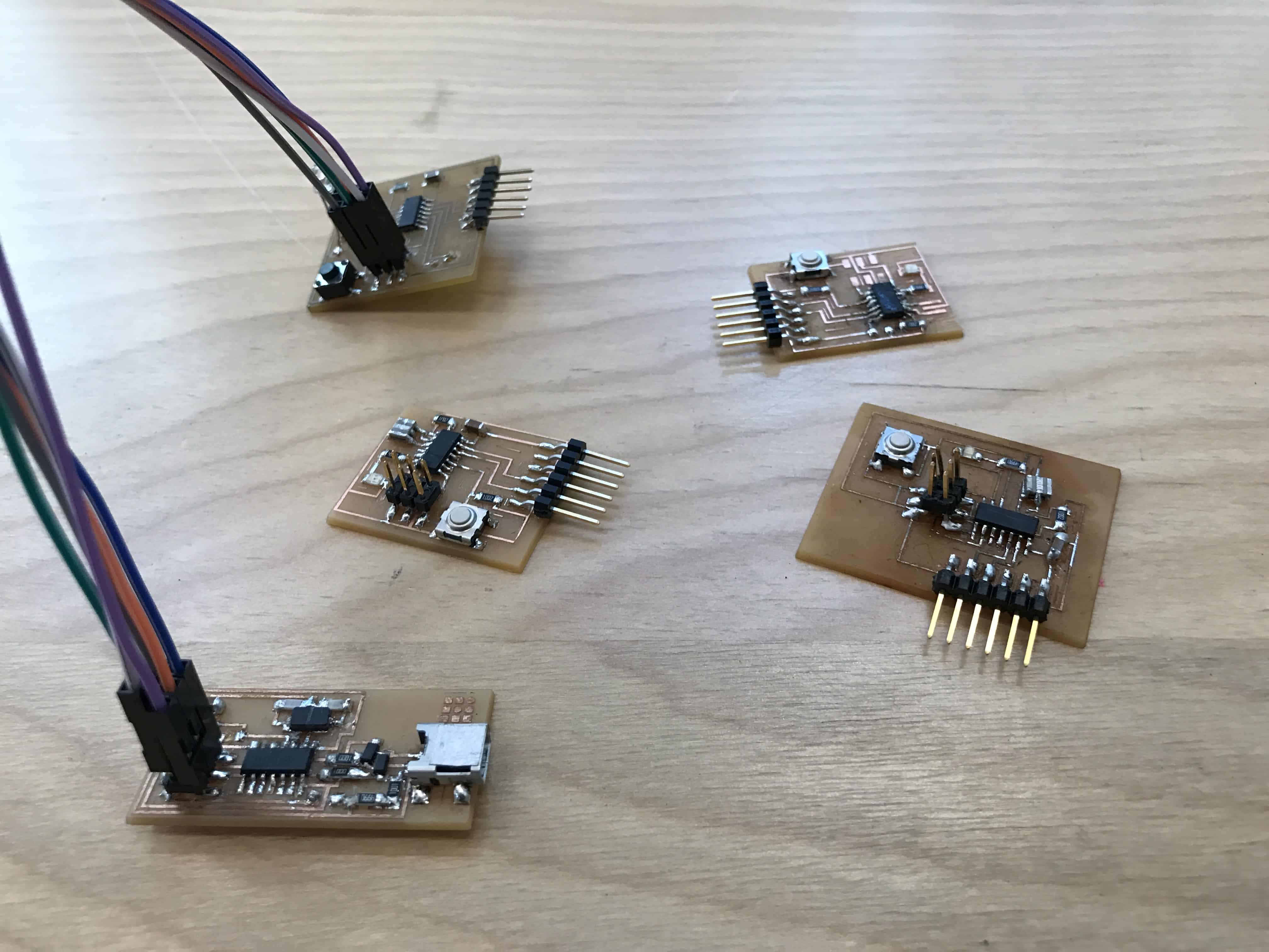
Here's the last phase on Fab Modules and the final result with all the parts solder on it!