WEEK 10
OUTPUT DEVICES
ASSIGNMENT
- Add an output device to a microcontroller board you've designed and program it to do something
Preperation
This is week assignment is to make a microcontroller board which can be used to contol an output device. There are different type of output devices are available like LED, Speakers,LED arrays, RGB LED, LCD,OLED,Servo & steppr motors etc. I have decided to make a contol board to interface with LCD and OLED. Actually for my final project, i need to display the measurement values for that my intitial planning is to use LCD as the display but the size of it is big, So i am planning to make it on OLED display. I thought this week will try the two displays , gone through the basics of LCD and OLED displays and the datasheet.
Multi Interface Board(MI Board)
I planned to make display contol board, especially for LCD and OLED display based on Attiny44 Microcontroller, Later i planned to brought some free pins to connectors so that i can control some more devices and named my circuit as Multiinterface board. Using the board we can interface LCD, OLED, Servos directly & by adding another driving board we can interface steppers and spaekers. My board block schematic is shown below.
Design of MI board
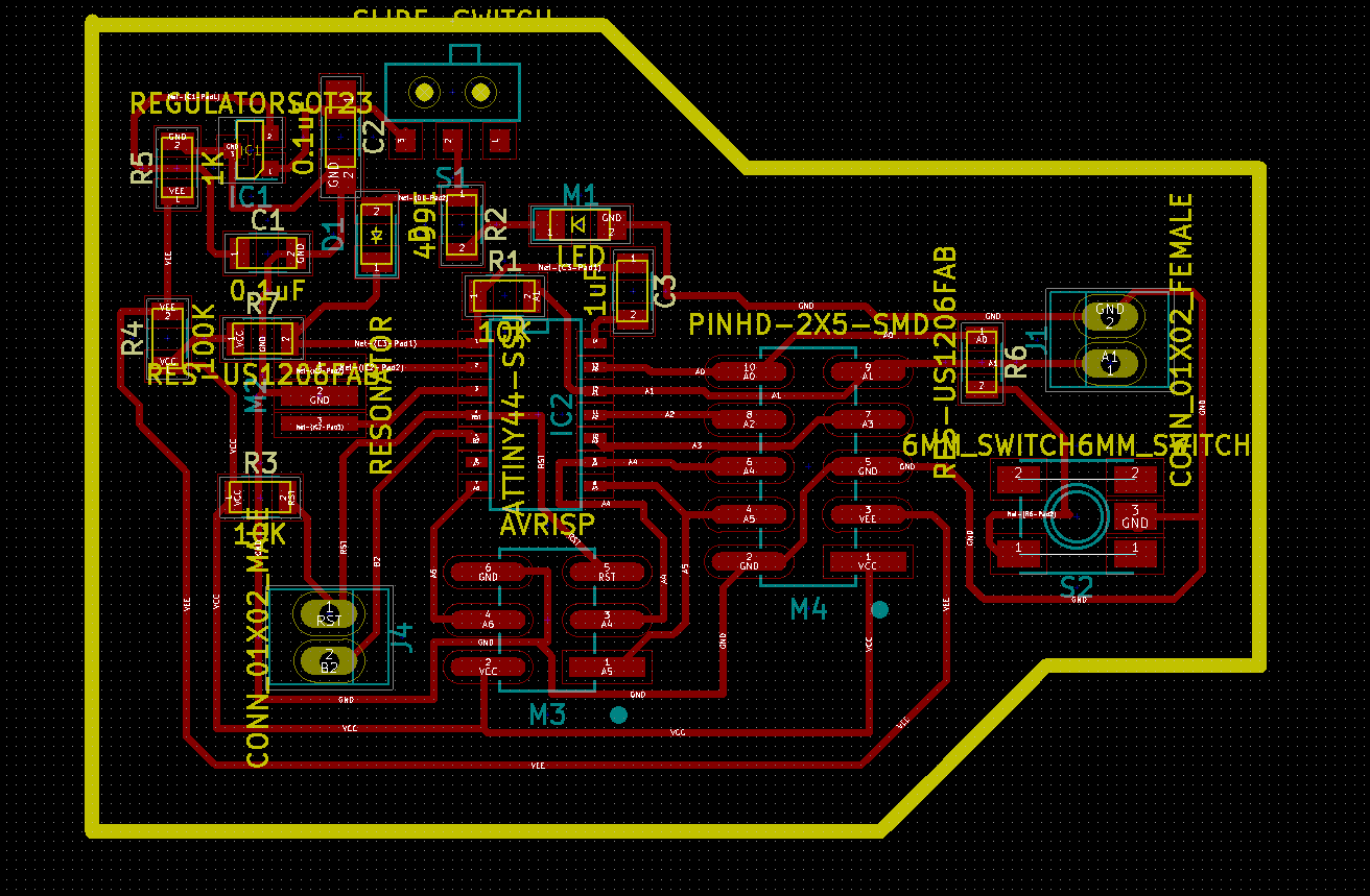
The board design i have done based on Neil's LCD board. This week i tried Kicad software for designing the board because in the electronics design week i have tried Kicad and interested to do something for my assignments. Started my boards design in Kicad schematic editor, First i downloaded and added the Fab libraries into the kicad libraries Fab library. Download the file,unzip it and add the ".lib" file to through componenet libraries option from the preference menu , Also i have gone through some video tutorials on designing usig Kicad. We can place the componenets using "place component" option from the right side of the toolbar.
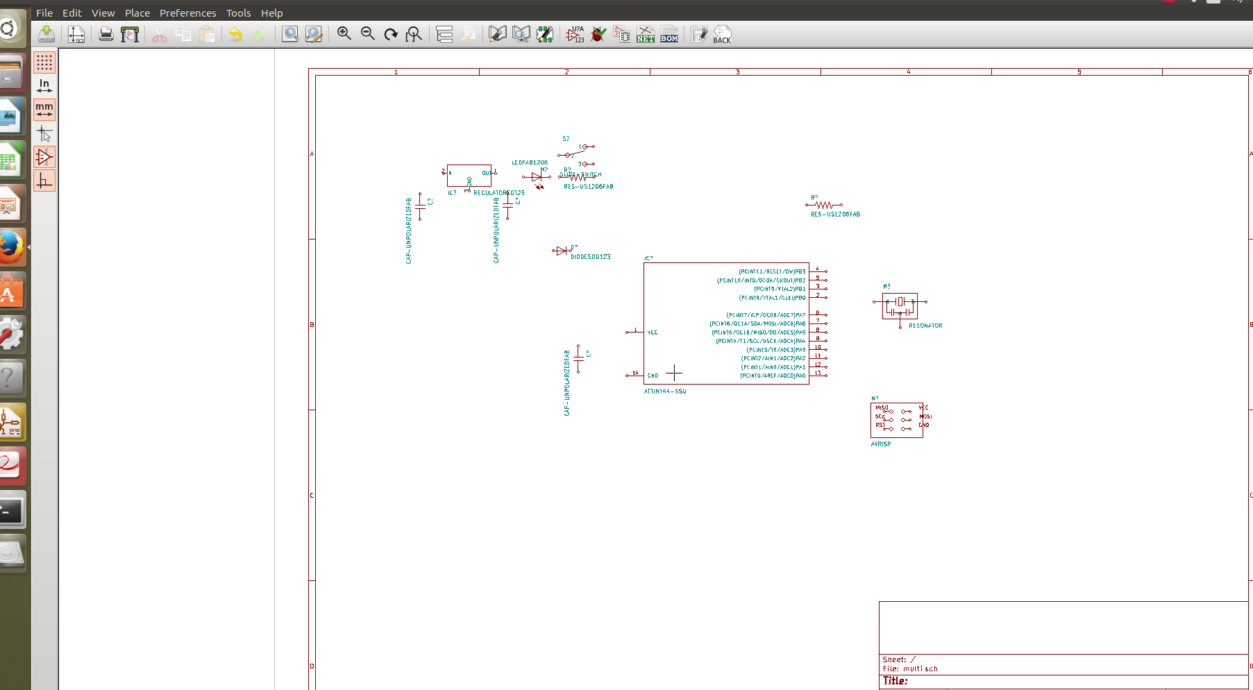
Actually as told earlier , My board is having some more circuits included a sensing circuit for the resistance value measurements and a voltage regulator circuit for standalone operation of the board. After placing all the componenets, connected the componenets each section and completed the schematic of my board. Next i have done the ERC checks and it showed some errors like opened connections etc., corrected those errors and the below showed image is the final schematic of my Multi Interface board.
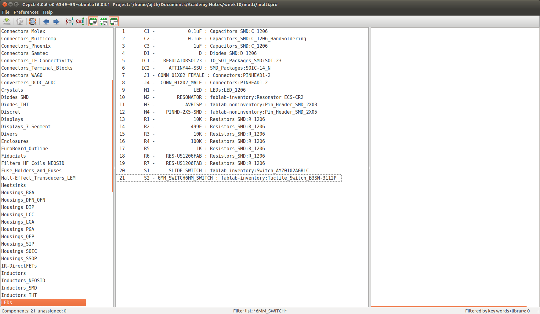
Next is to add componenet footprints, Once the schmatic is over we can add the foot prints of the components by "Run Cvpcb" button on the top menu. I have added the following footprints to my board.
After completing the step we can save the netlist and close the window. Again from the schematic editor generate the netlist using "Generate netlist" button and save into the directory.
Next step is to routing the layout of my pcb, We can select Run pcbnew button in the schematic editor for this. Once clicked the new window will come and we can import the netlist saved into the
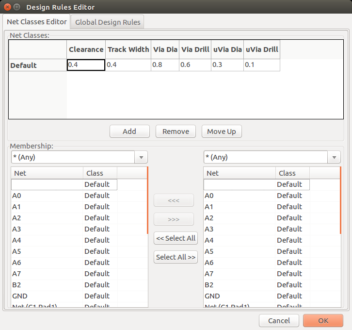
directory and open it. We have to first set the design rules from the "design rules" menu. My design rule setting for the multi control board is shown here.
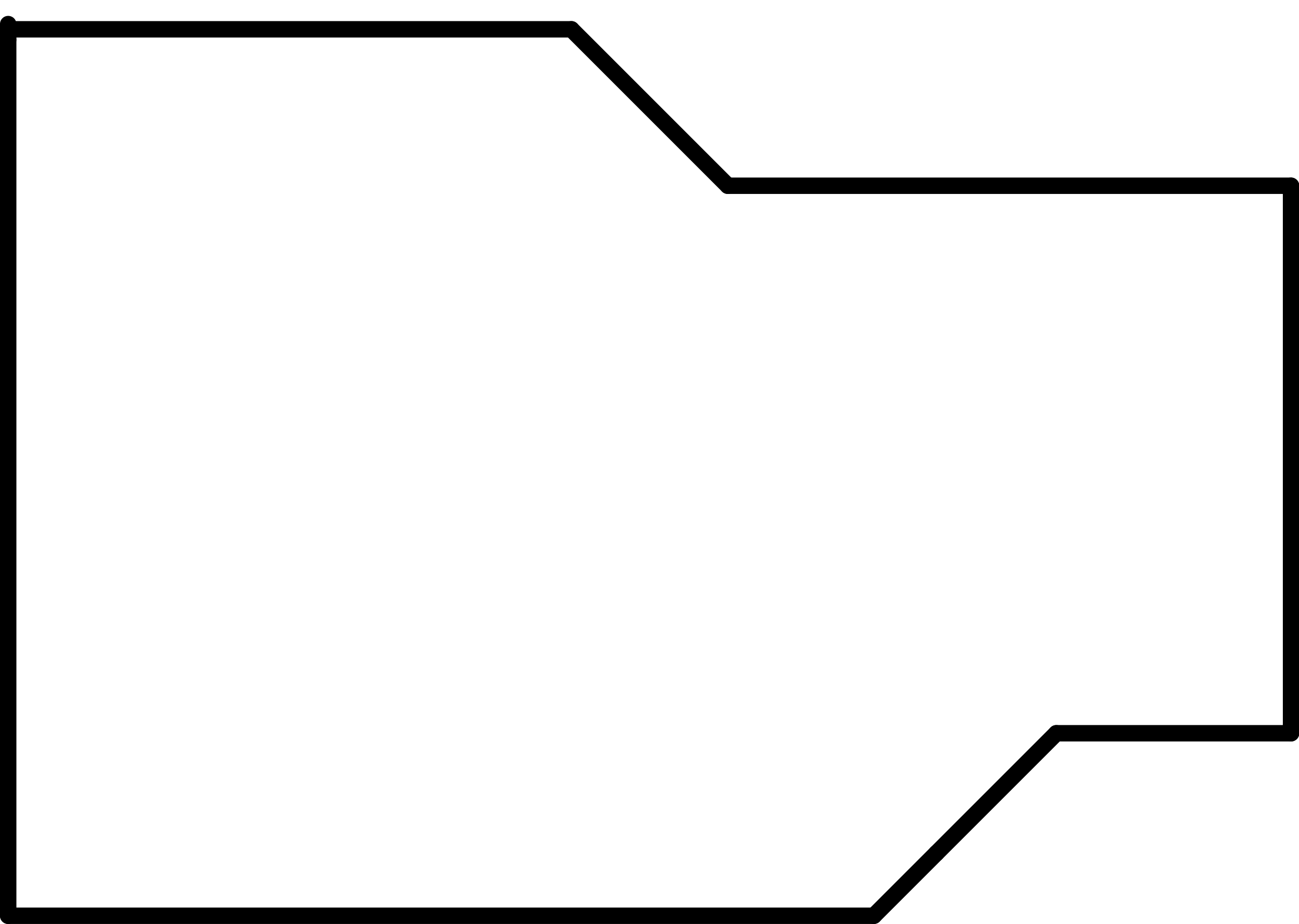
Set the desgn rules and we can do manual routing. It's one of the hardest part i have faced in this week, eventhough i enjoyed it. completed the layout routing and is shown below. This is a single side pcb and the red lines are the traces and the yellow lines are dimension lines.
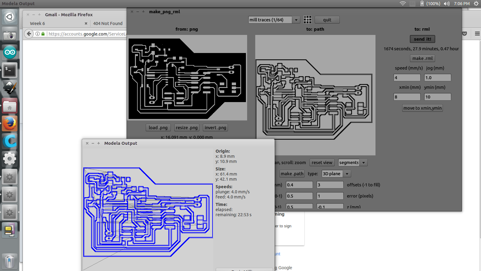
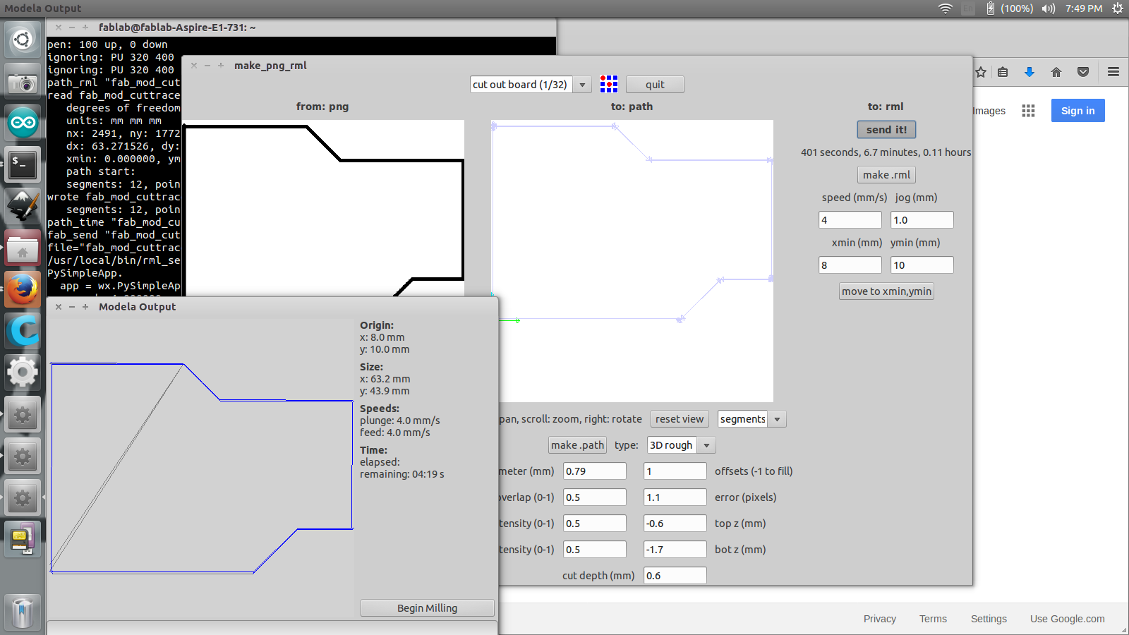
After the completion we can export the layout to ".SVG" format. First we need a file for milling the pcb and second one for cutting the board. The settings for the mill and cutout are shown below.
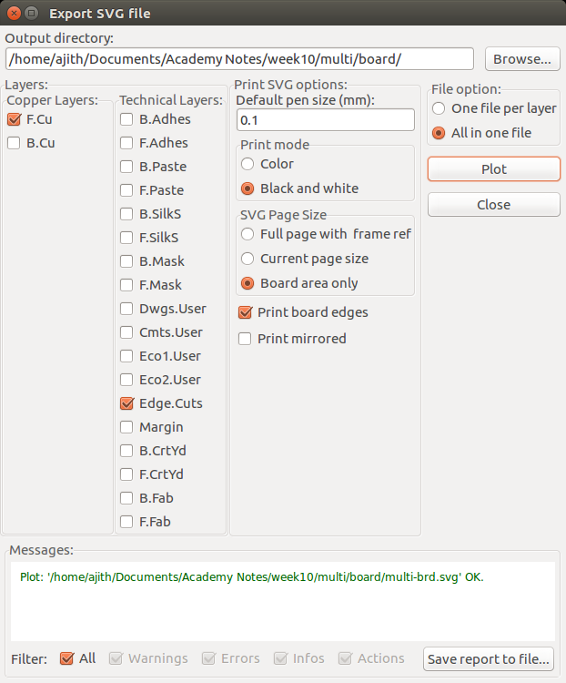
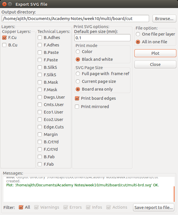
Exporting the milltraces Exporting cutout traces
Milling the PCB
The exported file need to be preprocessed inorder to mill it on Modela CNC, for that i have opened the files in gimp and done the edits and my final mill traces and cutout traces ".png" file is showed below.
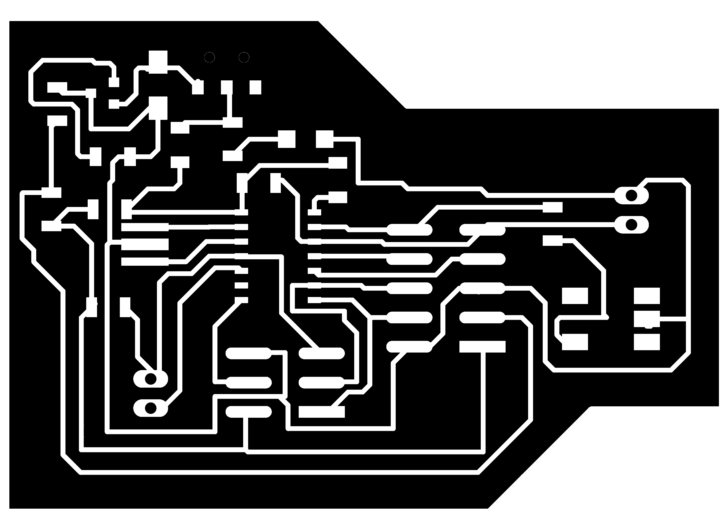
Milltraces(.png) Cut traces(.png)
Fabricating pcb in Modela
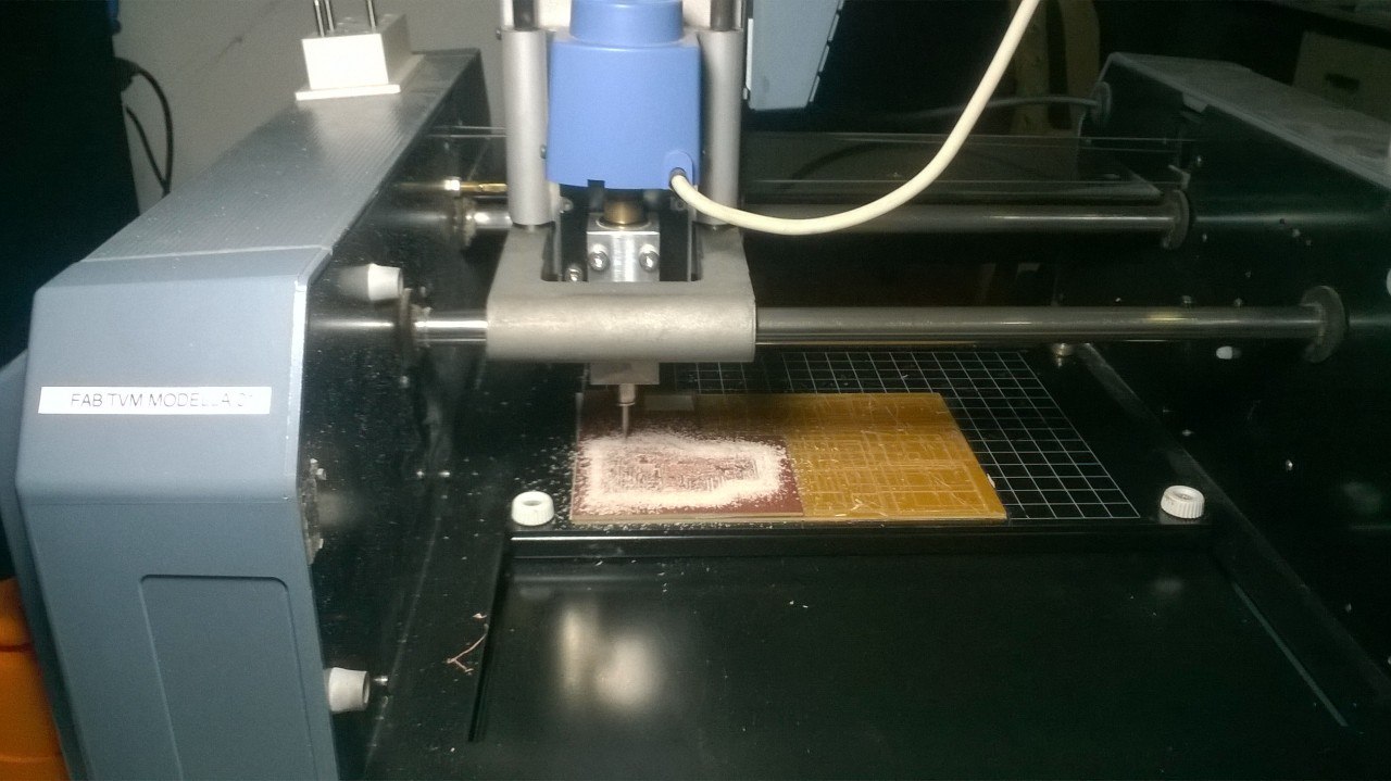
Milling the pcb requires two files of .png file format , one is for milling the pcb and the other is for cutting the pcb. I have saved the two files, this time i used the compiled version of fab module for processing the board in modela , beacause our pc installed with local version of current version fabmodule is under maintenace. I have done all the machine settings what i have done in electronics production week. Here i am adding some screen shots of the fab module processing steps of milling and cutting my pcb.
The image shown below is the shots taken while doing my pcb fabrication with modela. Used 0.4mm bit for milling and 0.8mm bit for cutting the pcb. Processing my board in Modela is shown below.
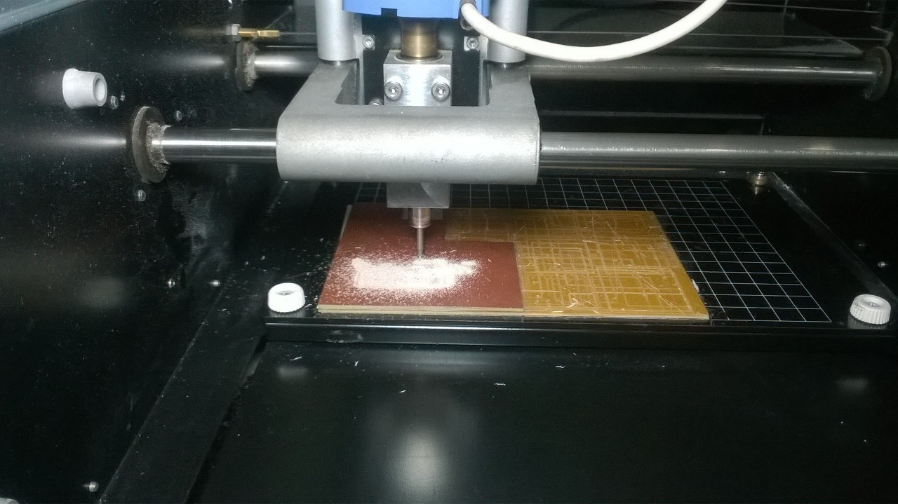
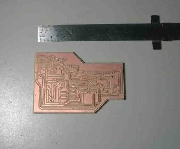
My pcb after milling the pcb is shown below.
Soldering the PCB
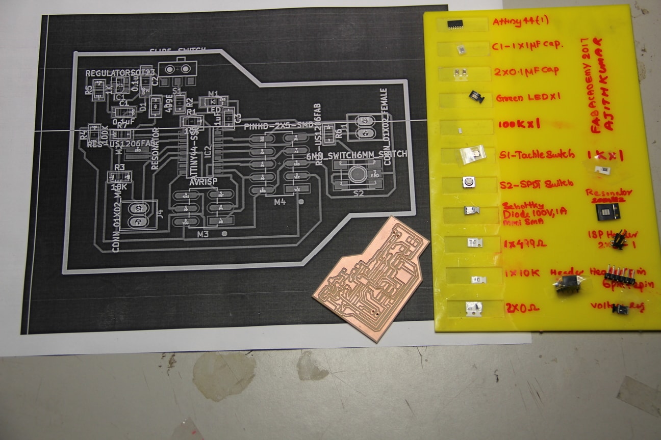
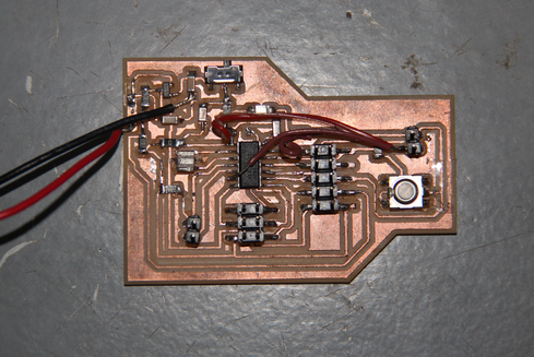
Prepared all the bill of materials required to soldering the board, collected and arranged in the plate and moved to the workbench, using soldering iron and lead soldered the components by refering the printed schematic of my Multiinterface board as shown below.
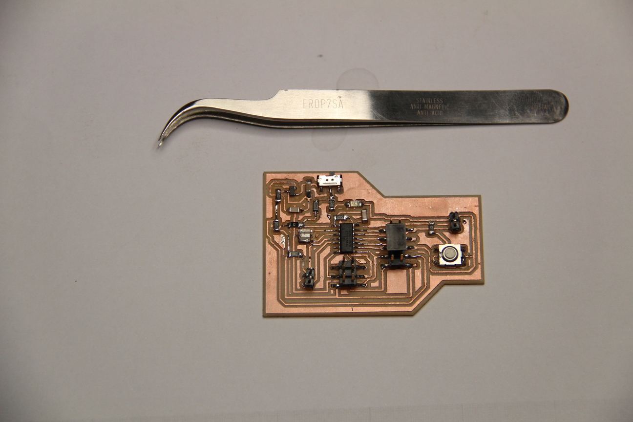
Soldered all the componenets and verified the orientation and polarities of componets etc. Hero shot of my soldered MI board is shown below.
Problems faced
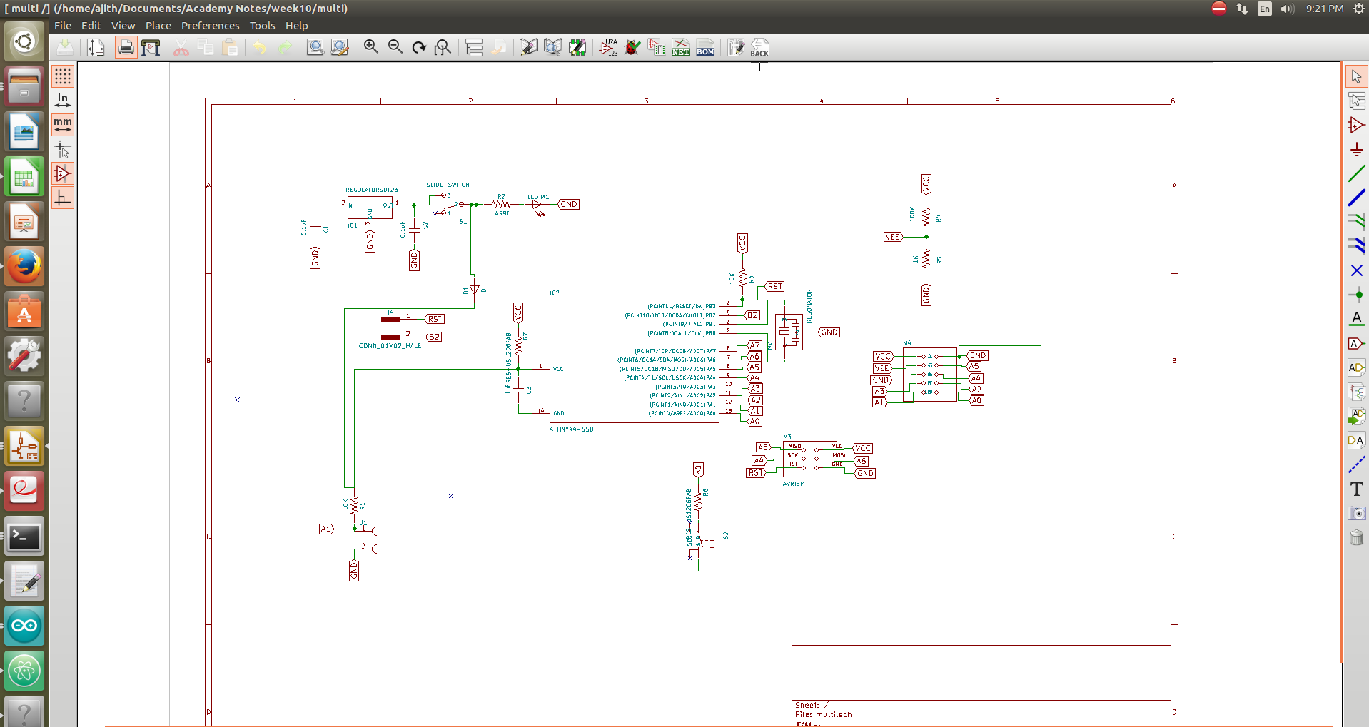
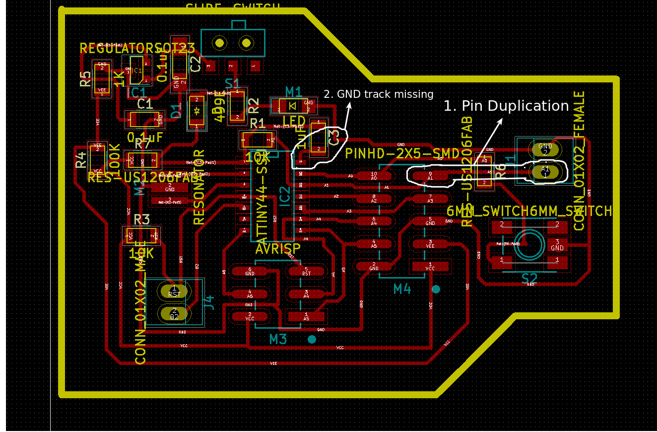
1. After soldering the board, checked once again the design at that time i found that the pin on A1 pin of attiny is being used for the sensing the resistance value. The mistake i made is shown below, it was the mistake in my schematic design. Inorder to correct that i have done some track cutting and wire jumper to seperate the resistance sense circuit and connected to Port A6 of Attiny44.
2. The second mistake i made is the GND track was open at the GND pin of Attiny 44. Iorder to solve this i put a wire jumper to the nearby GND tarck close to pin no.14 of Attiny44. The final circuit after correction is shown to the left of the schematic image.
Download Multiinterface board files (.zip)
Programming the board
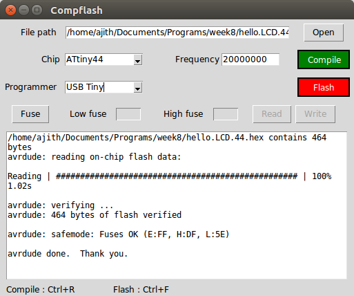
After correcting the issues i just copied Neil's LCD code to contol the LCD in 4 bit mode, this is just for testing my board. Saved the program from the archieves and edited using atom editor and programmed using compfalsh. The programming steps shots are shown below.
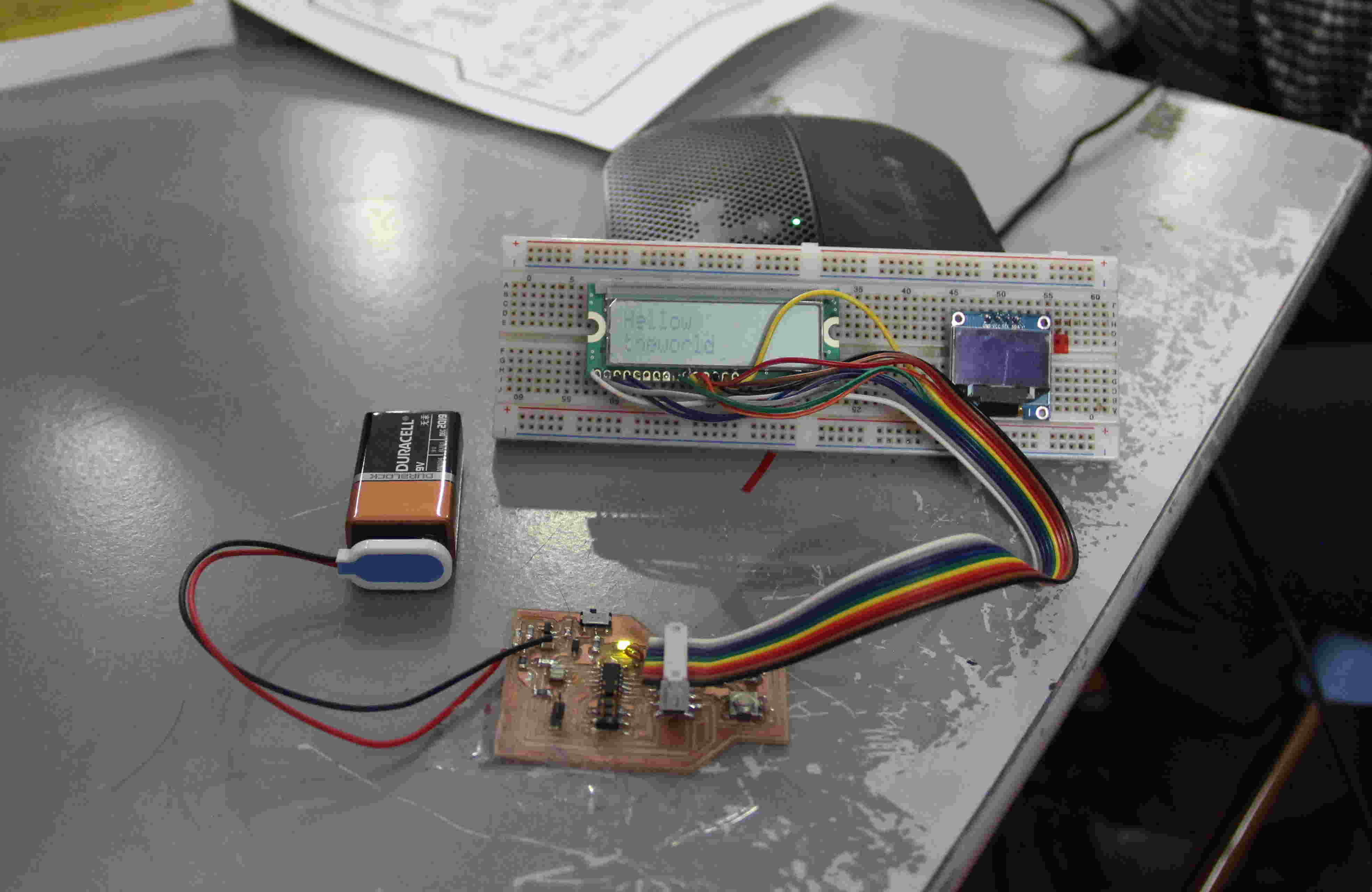
On successfully fusing the program into my board i have removed the ISP cable connection from my borad and connected 9V battery and turned it ON using the slide switch SW1 according to the design , this time the Green LED indicator will
glow and the LCD starts showing the "Hellow the world" text in the display. The LCD display connections are made by refeing the data sheet of the LCD and made a cable to connect it with the control board.
The output is shown below.
Programming the board using Arduino
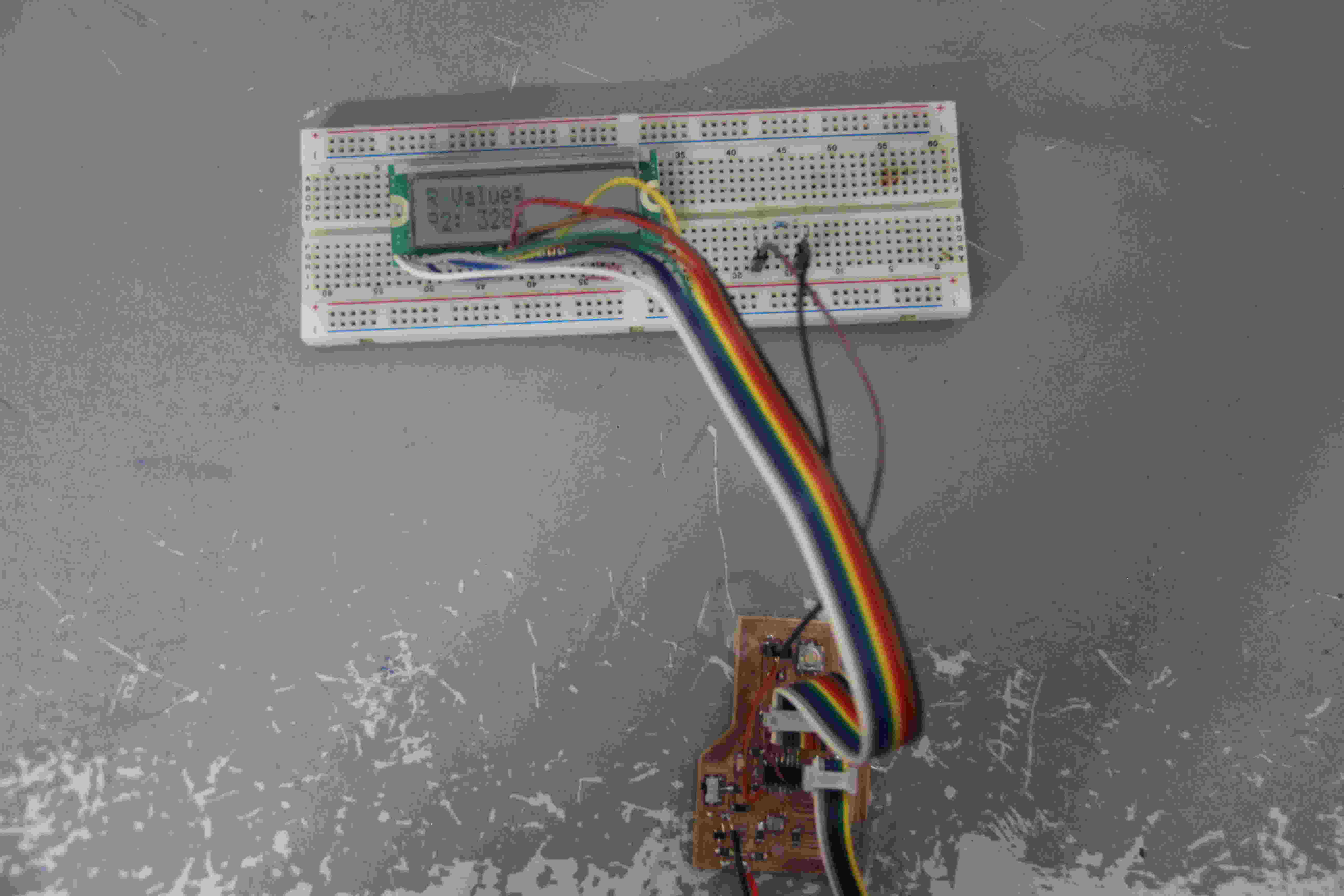
After testing my board with Neils code , I understand the code in detailed and moved to arduino to program my board to display the value of the unknown resistance. Started some example programms with arduino and written the code to display the value of the unknown resistance. The code is shown below.
# Resistance Meter Program #includeLiquidCrystal lcd(5,4,3,2,1,0); int analogPin= 6; int raw= 0; int Vin= 5; float Vout= 0; float R1= 10000; float R2= 0; float buffer= 0; void setup() { lcd.begin(16, 2); } void loop() { raw= analogRead(analogPin); if(raw) { buffer= raw * Vin; Vout= (buffer)/1024.0; buffer= (Vin/Vout) -1; R2= R1 * buffer; lcd.setCursor(0, 0); lcd.print("Vout: "); lcd.print(Vout); lcd.setCursor(0, 1); lcd.print("R2: "); lcd.print(R2); delay(1000); } }
After compiling the program in Arduino IDE fused the program to the Attiny44 through fab isp and i have tested it with a 330ohn leaded resistor. The out put is shown below.
Download Resistance measurement program file (.zip)
Quote of the Week
"You must do the things you think you cannot do"
by Eleanor Roosevelt