Electronics Production
Follow how I converted the FabTinyISP design file in Inkscape for Fab Modules, learned how to mill a PCB board, soldered the electronic components for my programmer, and programmed my board.
Summary
Our goals this week were to mill an in-circuit programmer by milling PCB, and then to complete the programmer by soldering the necessary components and programming the board.
Learning outcomes
Lessons learned
Links / Files
Components / Tools
Hall of Fame
References of Websites / Files
| # | References | Links/ Files | |
|---|---|---|---|
| 1 | Fab Academy Weekly Assignment- Electronics Production | LINK | |
| 2 | Building the FabTinyISP - Brian's Page | LINK | |
| 3 | Programming Your Board - Fab Academy Archive | LINK | |
| 4 | Building the FabTinyISP - Traces file | LINK | |
| 5 | Building the FabTinyISP - Outline file | LINK | |
| 6 | Building the FabTinyISP - PCB Board Schematic | LINK | |
| 7 | CrossPack for AVR Development - Download | LINK | |
| 8 | Xcode - Download | LINK | |
| 9 | Traces file - PNG / RML | PNG FILE | RML FILE |
| 10 | Outline file - PNG / RML | PNG FILE | RML FILE |
Electronics Components
| # | Component |
|---|---|
| 1 | 1x ATtiny45 or ATtiny85 |
| 2 | 2x 1kΩ resistors |
| 3 | 2x 499Ω resistors |
| 4 | 2x 49Ω resistors |
| 5 | 2x 3.3v zener diodes |
| 6 | 1x red LED |
| 7 | 1x green LED |
| 8 | 1x 100nF capacitor |
| 9 | 1x 2x3 pin header |
Designs
We used Brian's FabTinyISP tutorial and circuit board designs as a guide, and first had to use Inkscape and Fab Modules to prepare the trace and outline files for milling.
Lessons Learned- Design
| Tool | Lesson Learned |
|---|---|
| InkScape | When duplicating file, make sure to use "duplicate" command and not "copy/paste" otherwise the file is flipped. The file must be in the same orientation each time. (See image InkScape Step 1) |
| InkScape | Don't forget to add a third layer of a black rectangle to eliminate white boarder around trace/ outline files, otherwise it will show up in Fab Modules as another cutline. |
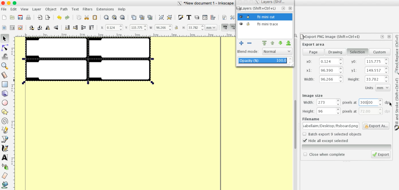
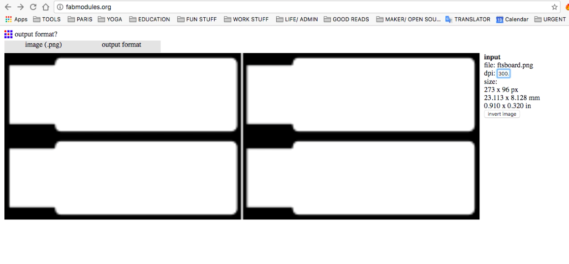
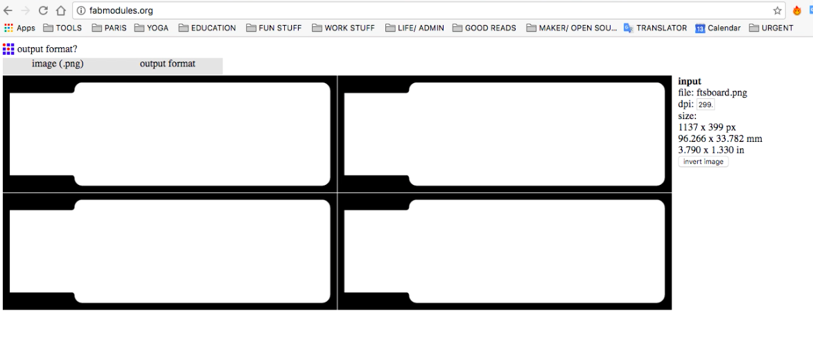
| InkScape | The resolution should be set to 1000 dpi, not 300 or 72. This can only be changed in Inkscape while exporting your file, not in Fab Modules, otherwise it will alter the dimensions of your file. |
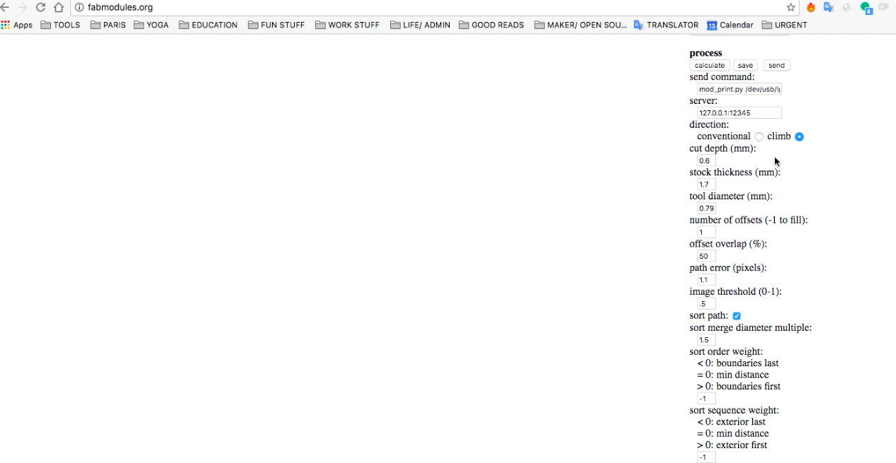
| Fab Modules | Make sure the X, Y, Z axis are all set to 0 before sending / exporting your file as .rml. Otherwise, the mill will use this location and possibly cut into your circuit board in the wrong area. |
| Fab Modules | Note that for the Outline File the cut depth should be 0.6 mm, and the stock thickness should be 1.7 mm |
Circuit Board Trace and Outline Files
| # | Reference | File | |
|---|---|---|---|
| 9 | Traces file - PNG / RML | PNG FILE | RML FILE |
| 10 | Outline file - PNG / RML | PNG FILE | RML FILE |
Using InkScape to Prepare the Trace and Outline files for Fab Modules
InkScape Step 1: Creating multiple layers in Inkscape for file
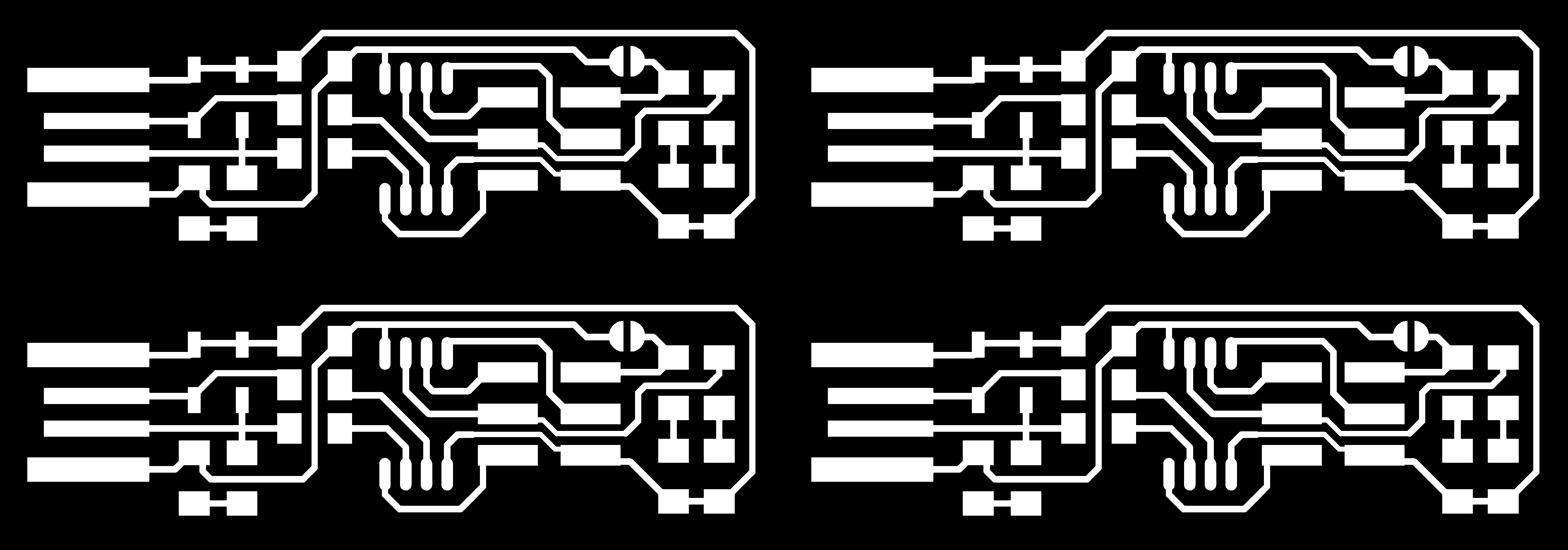
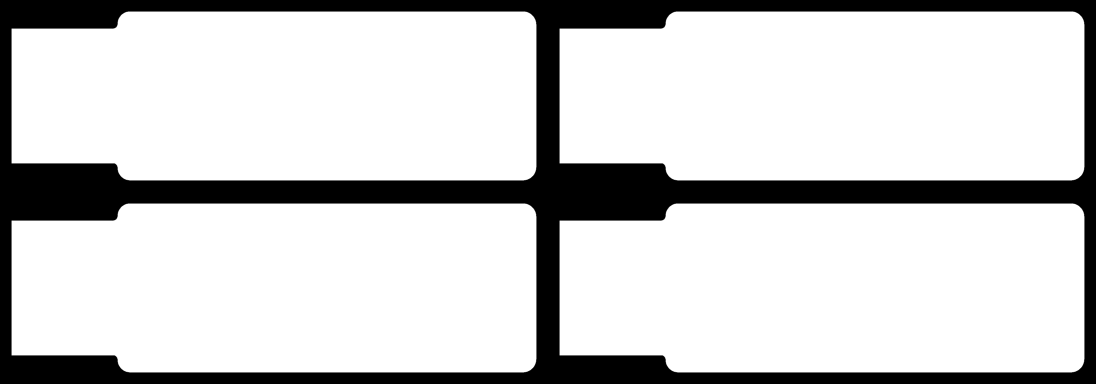
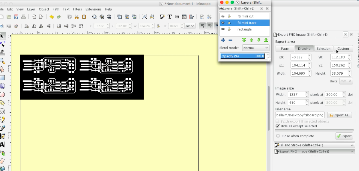
The first step is duplicating the trace file four times in a grid to optimize the layout of the desigfor the milling job, and to create multiple boards to practice with. Next, import and duplicate the outline file directly above the trace file in order to ensure the mill cuts out the outline of the circuit board correctly. Also, make sure to create a third layer of a black rectangle to avoid having the white lines between the four design show (see error 2 in Fab Modules Steps). Make sure to assign the trace, outline, and black rectangle to different layers as you will export each layer as a different file to upload in Fab Modules.
InkScape Step 2- Error in dpi pic
Notice that the resolution in this file is too low, this is due to not changing the dpi in Inkscpae when exporting the file. We made this mistake several times, first forgetting to change the dpi (so the default was 72), then by changing it to 300 (which was still too low), and finally getting it right by setting the dpi to 1000.
InkScape Step 3- Changing dpi in inkscape to 300
Here we changed the dpi to 300 to increase the resolution before exporting from Inkscape. Note that the resolution needed is actually 1000, not 300.
Using Fab Modules to Prepare Cut-File for Milling
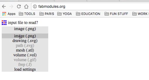
Fab Modules Step 1: Input file to read - .PNG
First, open Fab Modules and input your exporting .png file from Inkscape.
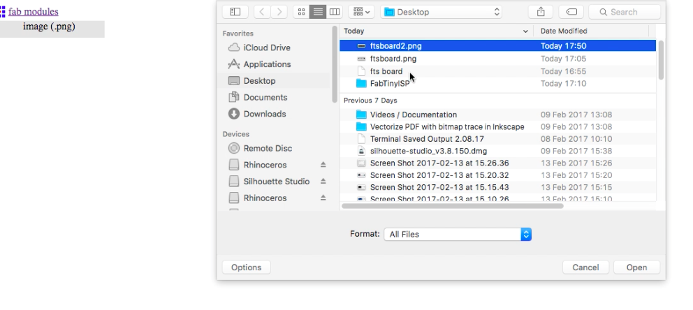
Fab Modules Step 2- Opening your file
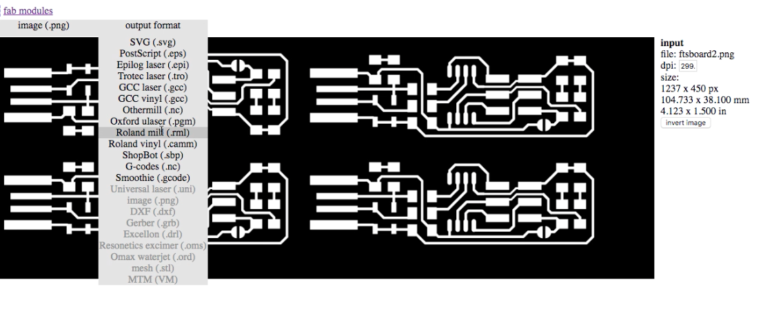
Fab Modules Step 3- Output format- Roland Mill
Next, select the machine used for the milling job, for us it was the Roland Mill.
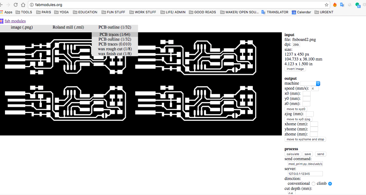
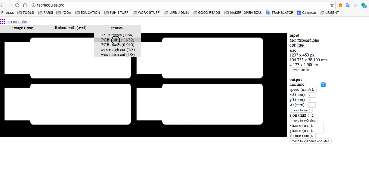
Fab Modules Step 4- PCB outline - PCB traces 1/64
Next, open your trace file and select the router bit size 1/64.
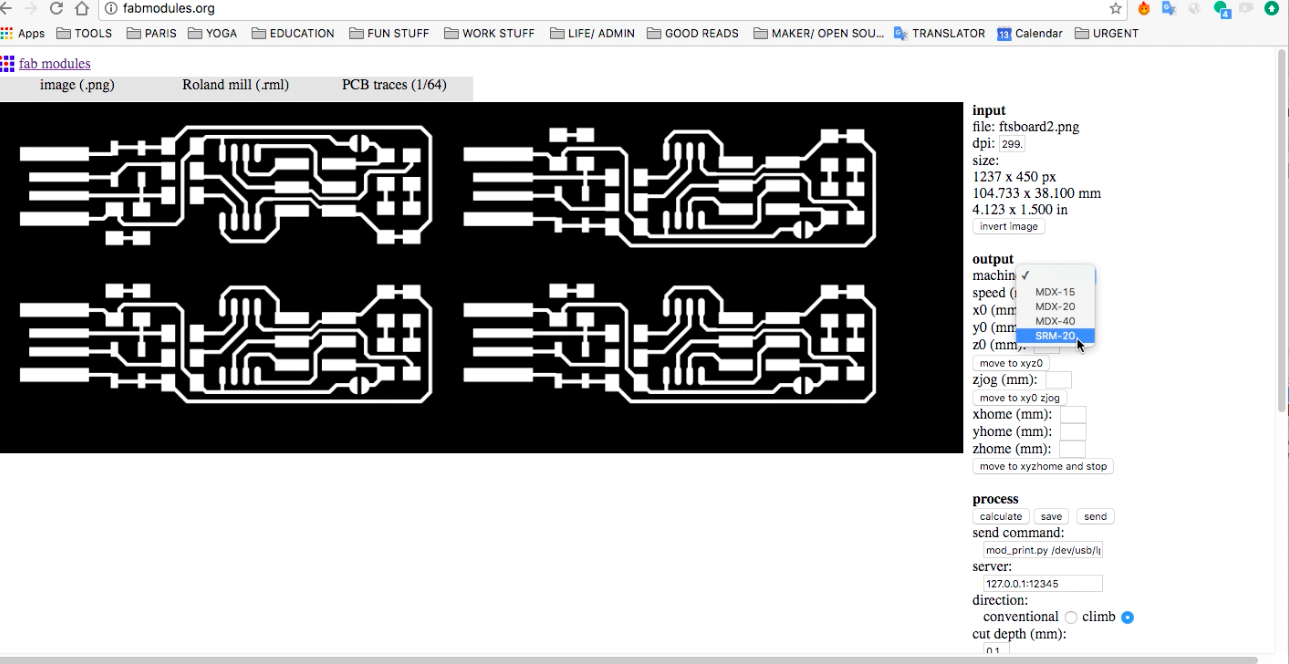
Fab Modules Step 5- Output- Machine- SRM20
Select the machine SRM20 for the pre-set tool/ cut information.
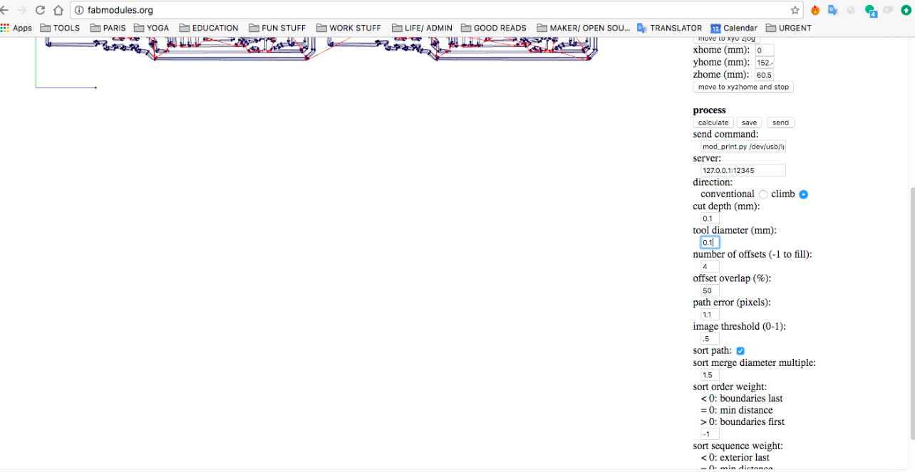
Fab Modules Step 6- Tool Diameter 0.1
Note- we had to change the tool diameter to 0.1 since we did not yet have the 1/64 bit.
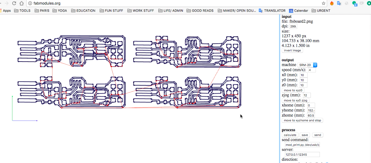
Fab Modules Step 7- Note Error- XYZ Axis 10, not 0
Note- the X, Y, Z axis should be set to 0, not 10. This caused the mill to cut into the trace file once we ran the outline file with the same coordinates set at 10, not 0.
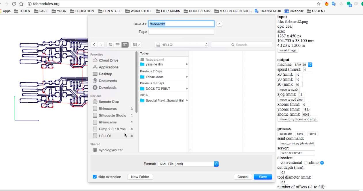
Fab Modules Step 8- Save your exported file as RML to send to Mill
Calculate your file and if it looks good, send it / export it as an .rml file to send to the mill.
Fab Modules Step 9- Fixing XYZ Axis- 0
We eventually realized the axis was set incorrectly to 10, so we went back and changed it to 0.
Fab Modules Step 10- Outline file- PCB Outline- 1/32
Next, upload your Outline file, select Roland Mill again, and the choose the PCB outline file at 1/32.
Fab Modules Step 11- Note Cut Depth/ Stock Thickness
Note that the cut depth should be 0.6 mm, and the stock thickness should be 1.7 mm.
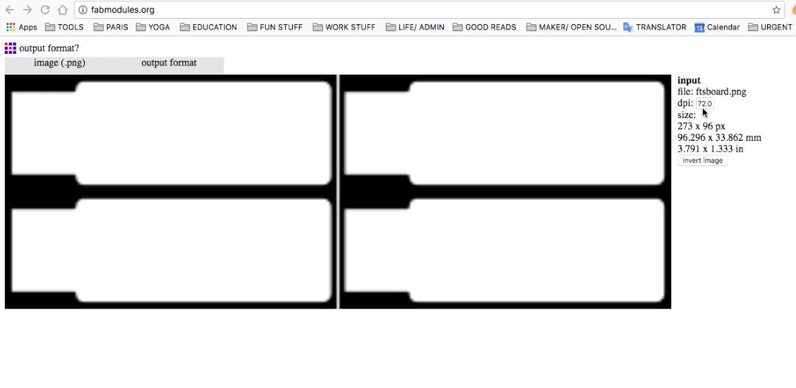
Fab Modules Error 1- Note dpi error- dimensions change
Note the low resolution as a result of not increasing the dpi in Inkscape before exporting the .png. We evenutally tried 300 dpi, and finally settled with 1000 as the correct resolution in the end.
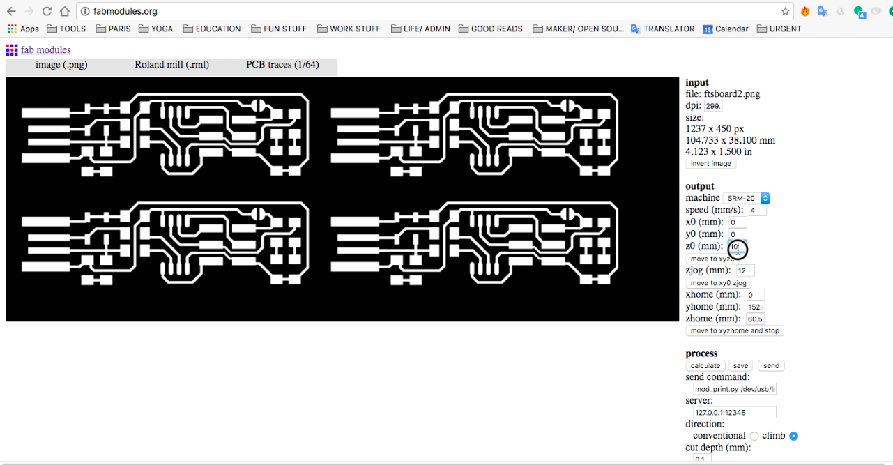
Fab Modules Error 2- White spaces between the boards
Note the white lines between the four board designs. This is an error from not initially adding the third layer in Inkscape of the black rectangle underneath the trace and outline layers.
Milling
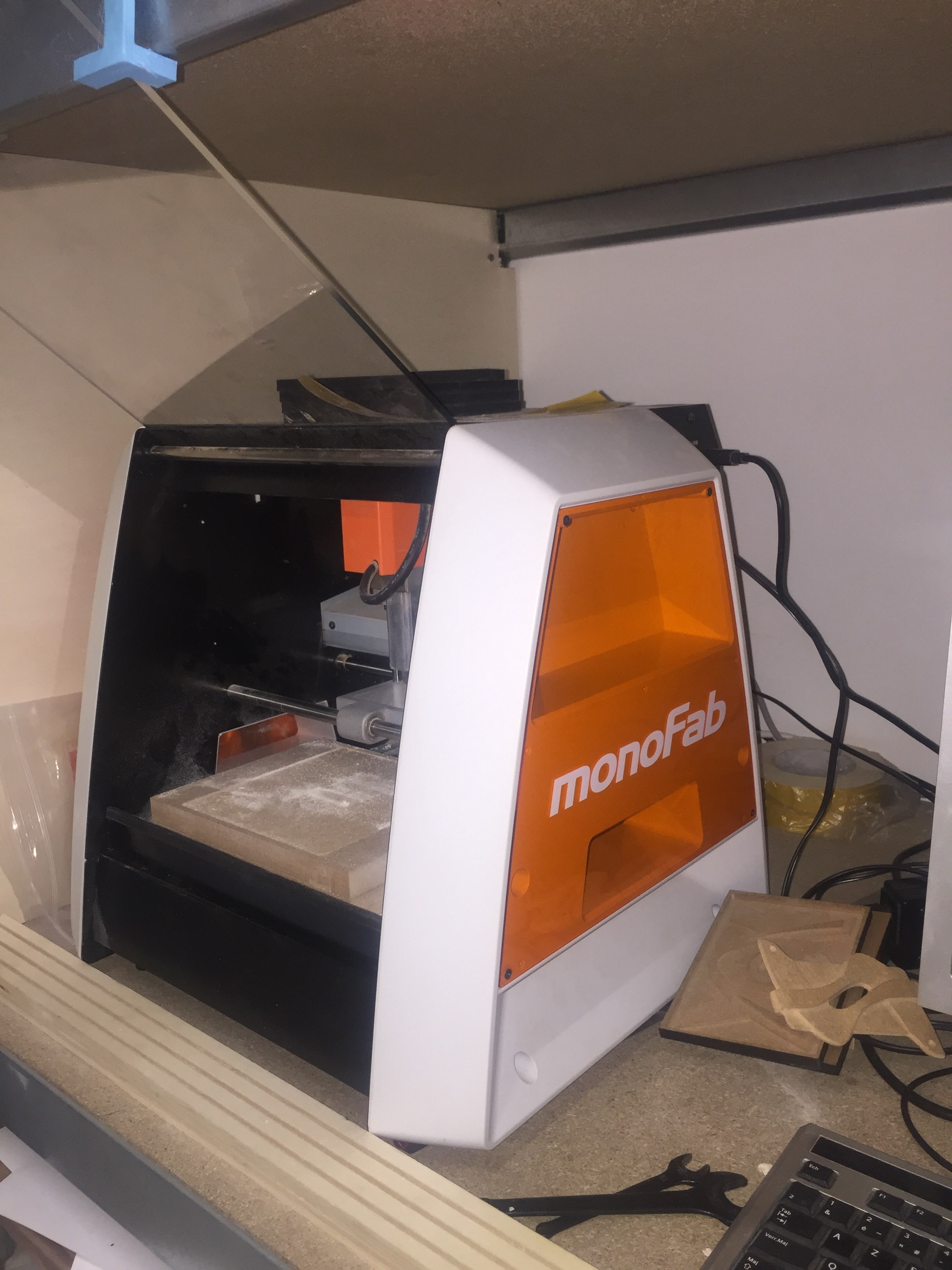
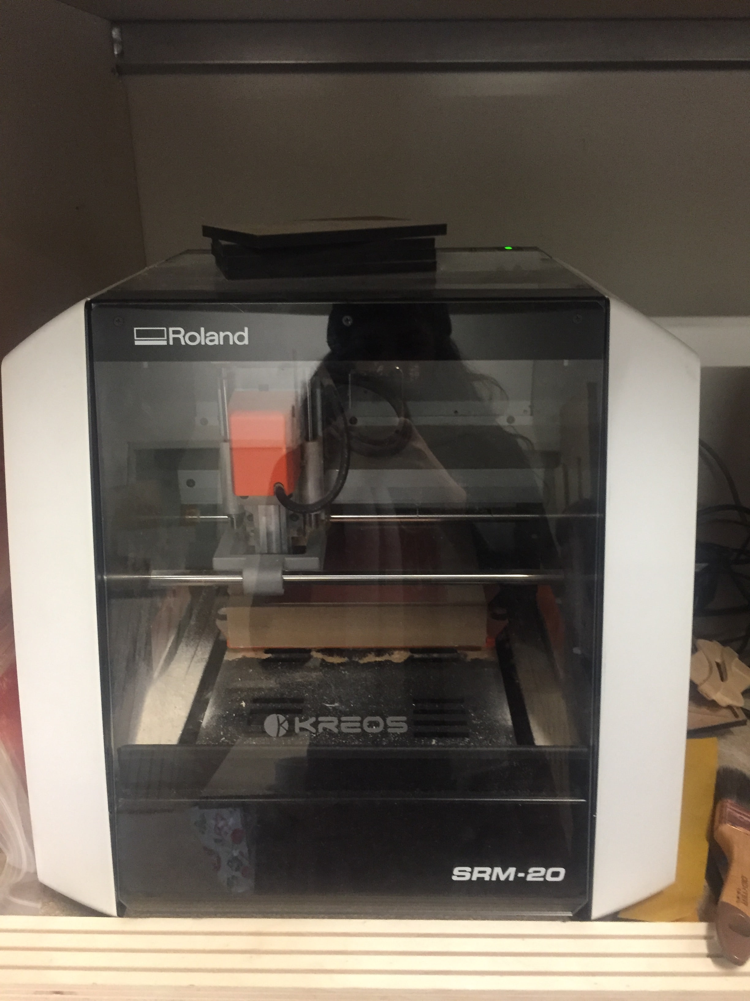
We used the Roland Mill SRM-20 to engrave and cut the trace and outline files for our circuit board into copper plated PCB.
Lessons Learned- Milling
| Tool | Lesson Learned |
|---|---|
| Roland SRM-20 | When changing the router bit, make sure to keep the cap on and hold the bit in place when unscrewing or tightening the joints, since the bits are very fragile and can break easily. |
| Roland SRM-20 | Make sure the double-sided tape on the sacrificial board and PCB board are perfectly aligned and not overlapping as this can cause either board to be unstable and possibly damage the cutting job. |
| Roland SRM-20 | Also, make sure to firmly press the sacrificial board and PCB board into the base of the mill, otherwise it may also become unstable and dmamage the cutting job. |
| Roland SRM-20 | Use the 'paper test' to ensure that the Z axis is well defined, otherwise the router may not cut all the way through the copper coating. |
Using the Roland Mill to Engrave and Cut our Circuit Boards
Milling Machine- Roland S20
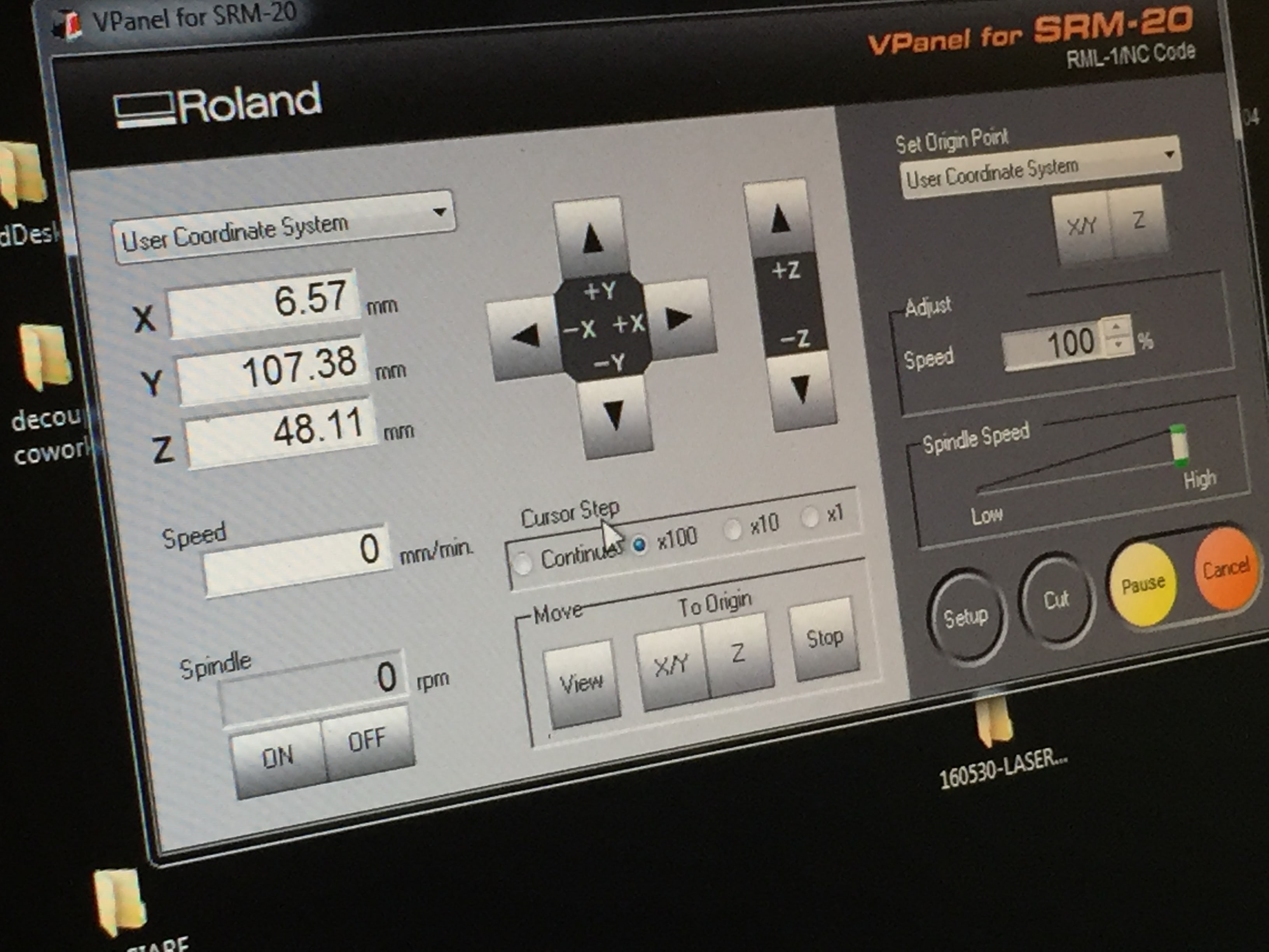
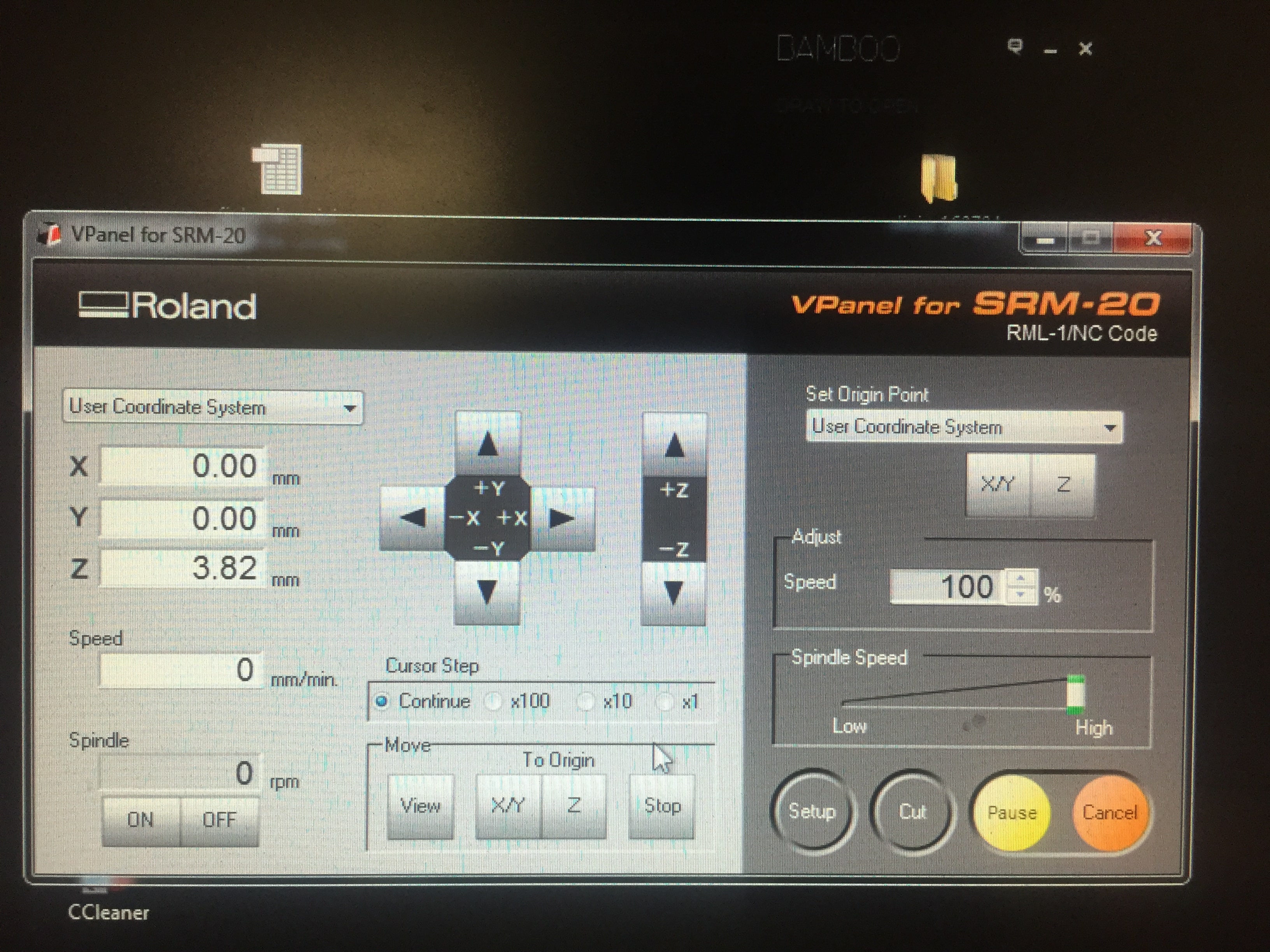
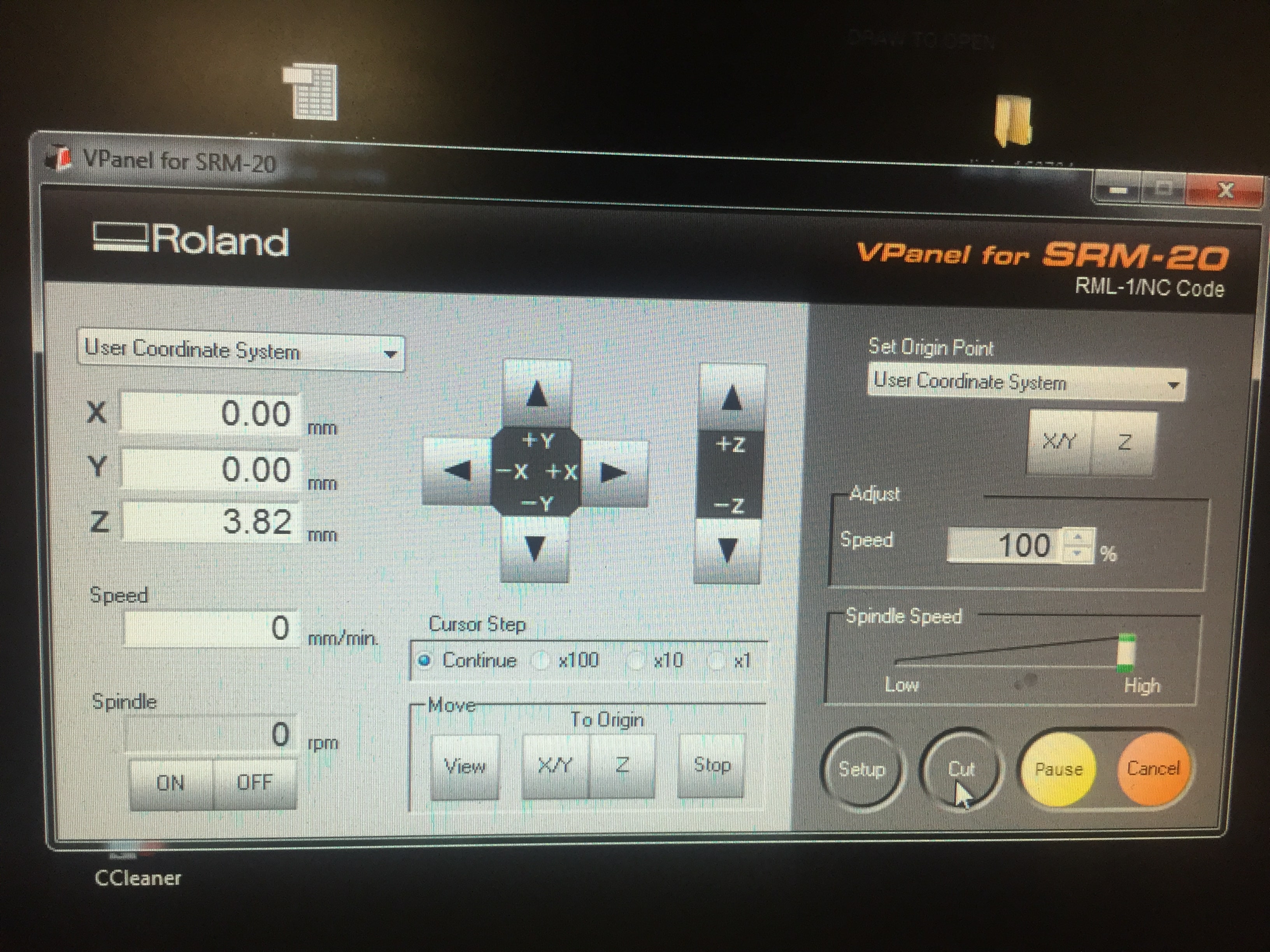
Roland Mill SRM-20 Interface
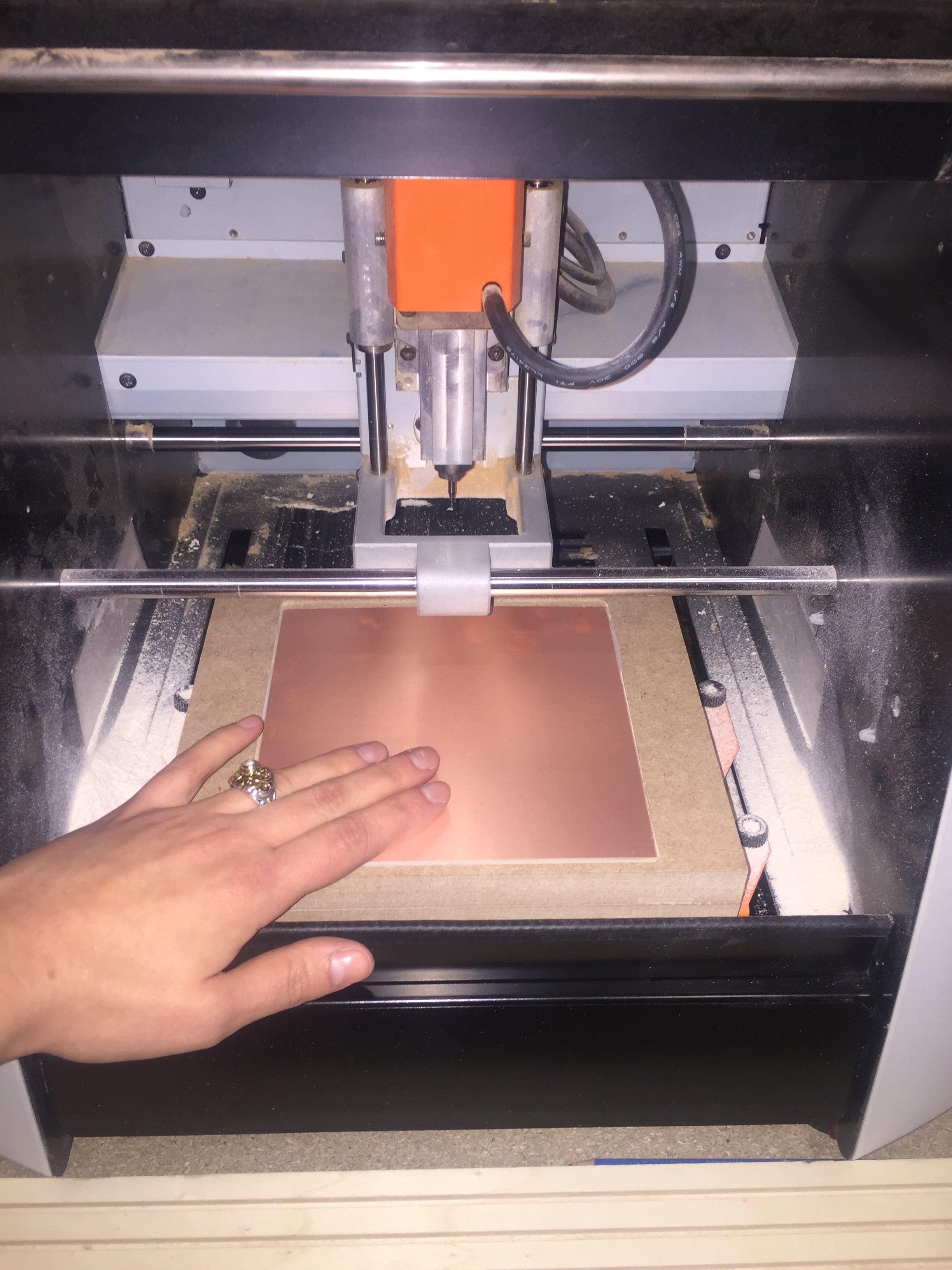
Milling Step 1
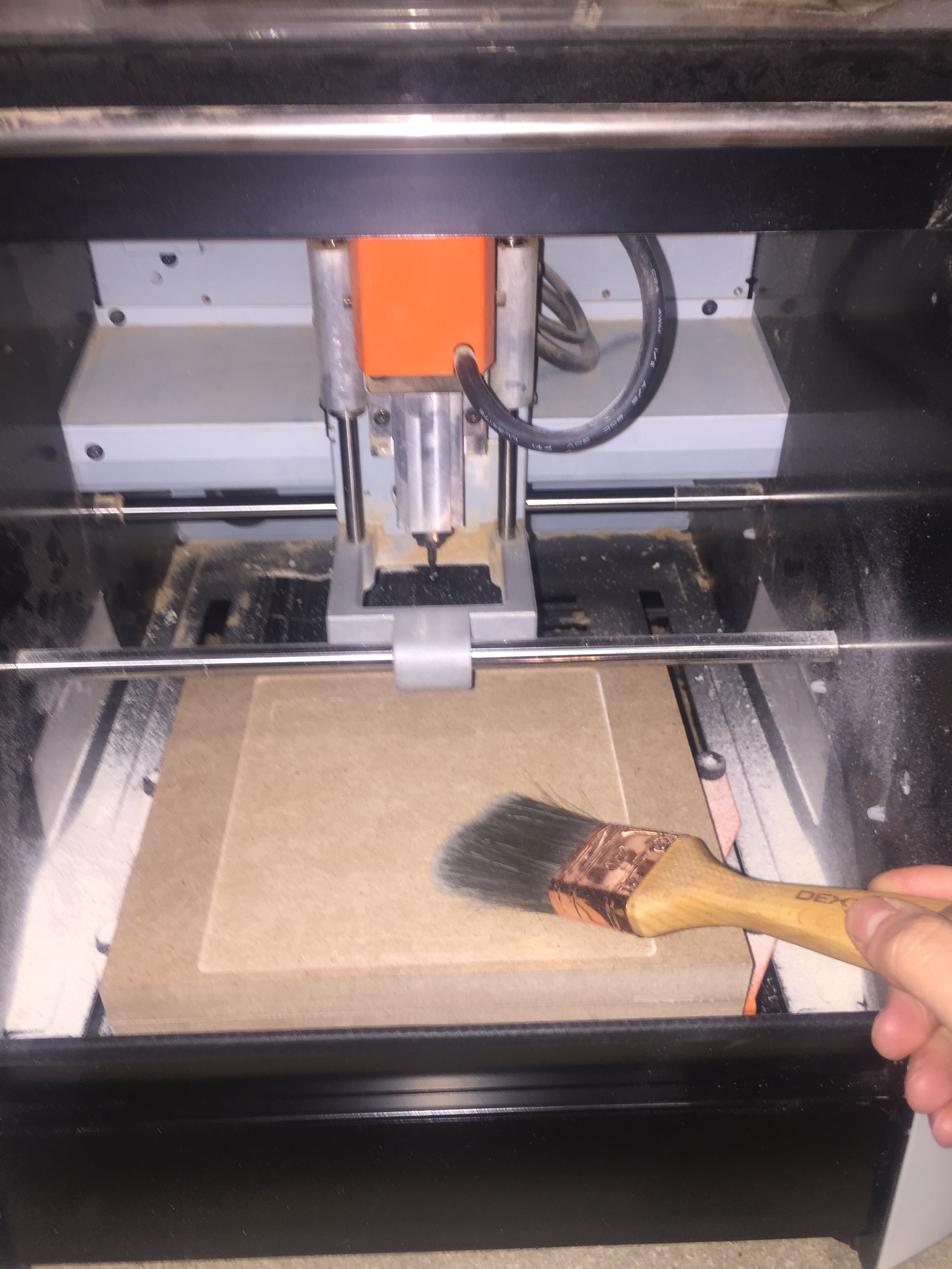
Clean off sacrificial board of dust and old PCB.
Milling Step 2
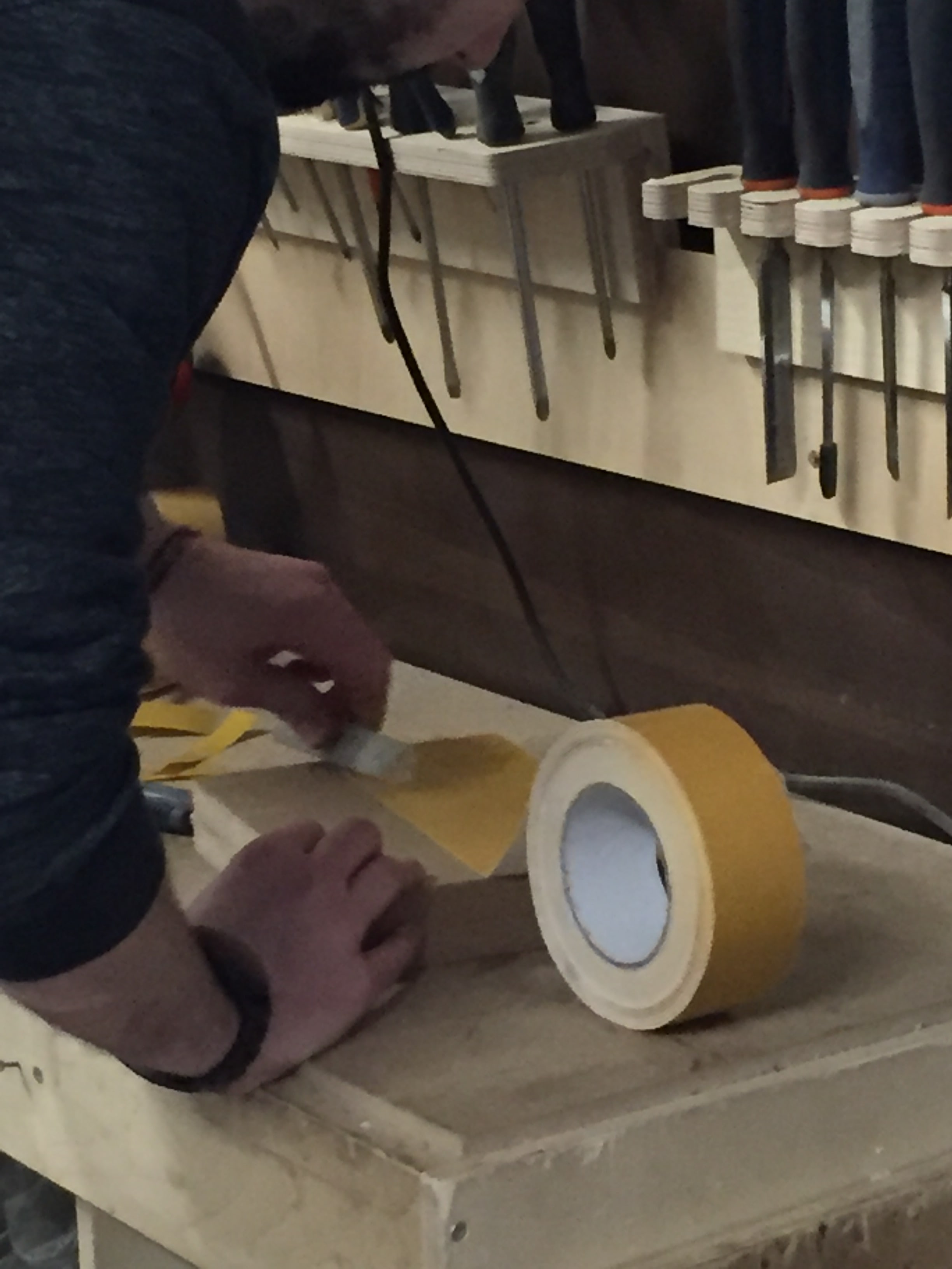
Ensuring well aligned taping of sacrificial board. Make sure the double-sided tape on the sacrificial board and PCB board are perfectly aligned and not overlapping as this can cause either board to be unstable and possibly damage the cutting job.
Milling Step 2.2
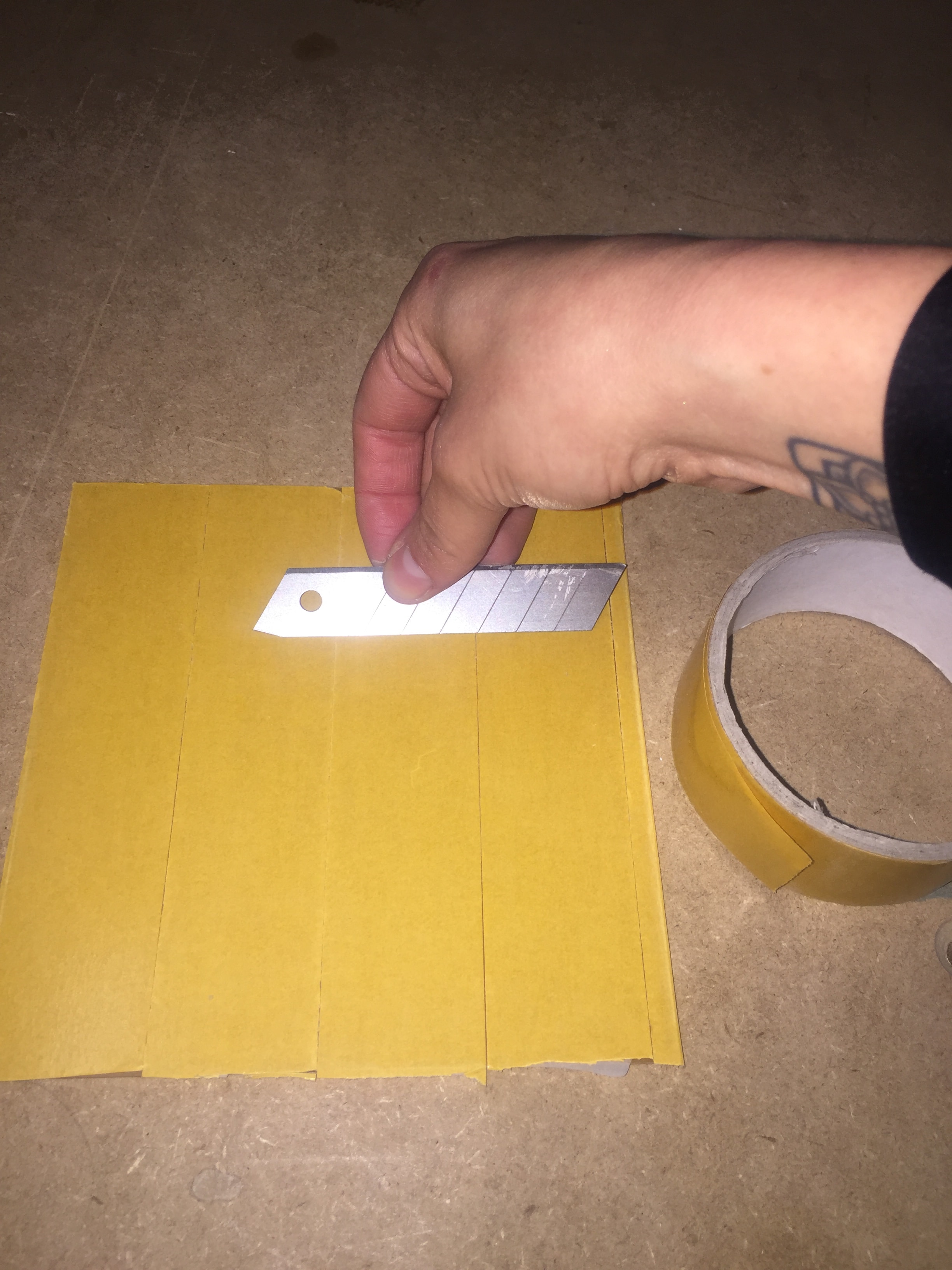
Double-Sided tape PDB board- flatten with sharp edge.
Milling Step 3
Firmly press and flatten the sacrificial board into the base of the mill, and the PCB board into the sacrificial board, otherwise both may become unstable and dmamage the cutting job.
Milling Step 4
Unscrew old router bit- When removing / changing the router bit, make sure to keep the cap on and hold the bit in place when unscrewing or tightening the joints, since the bits are very fragile and can break easily.
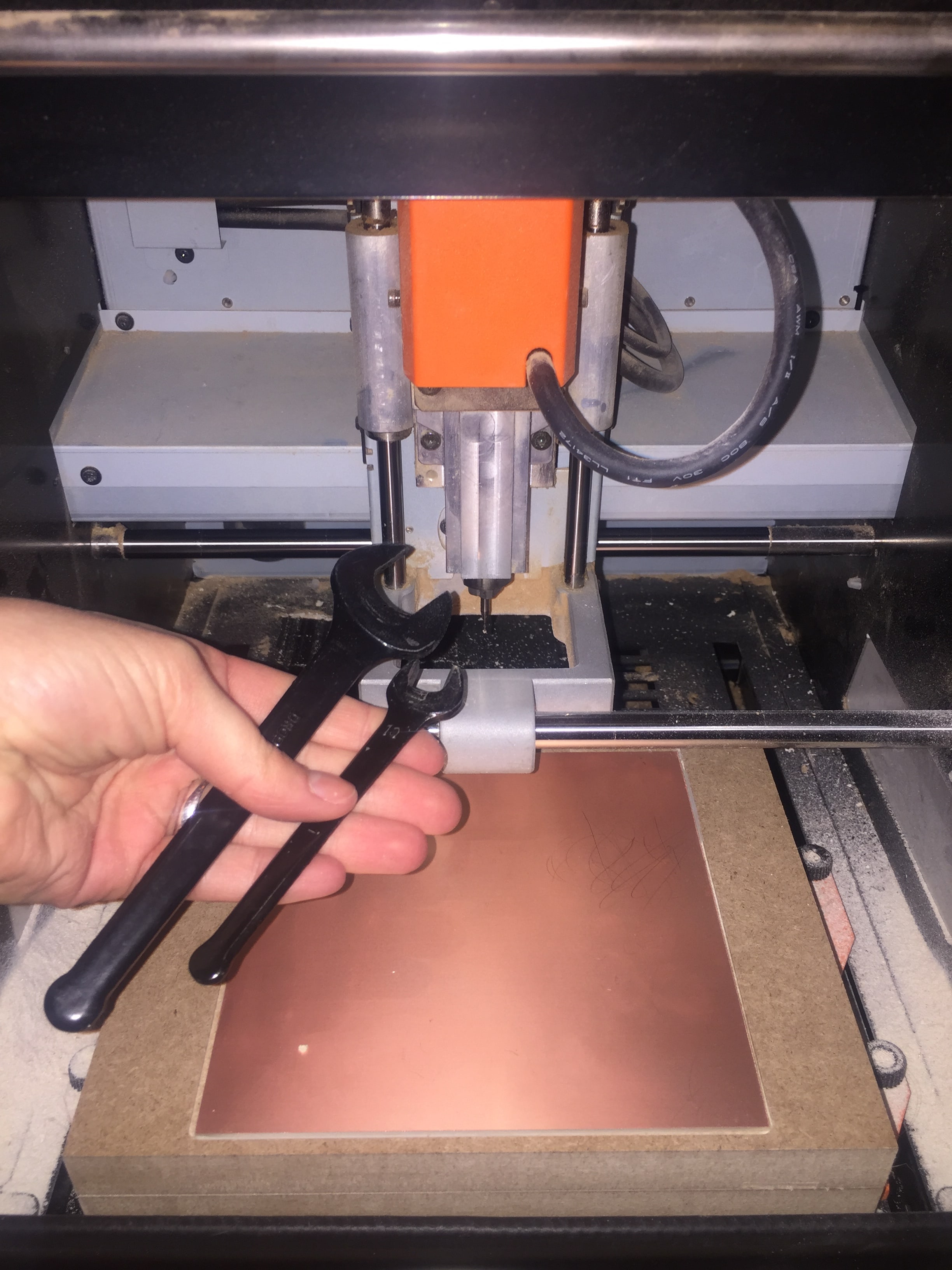
Milling Step 5
Change router bit.
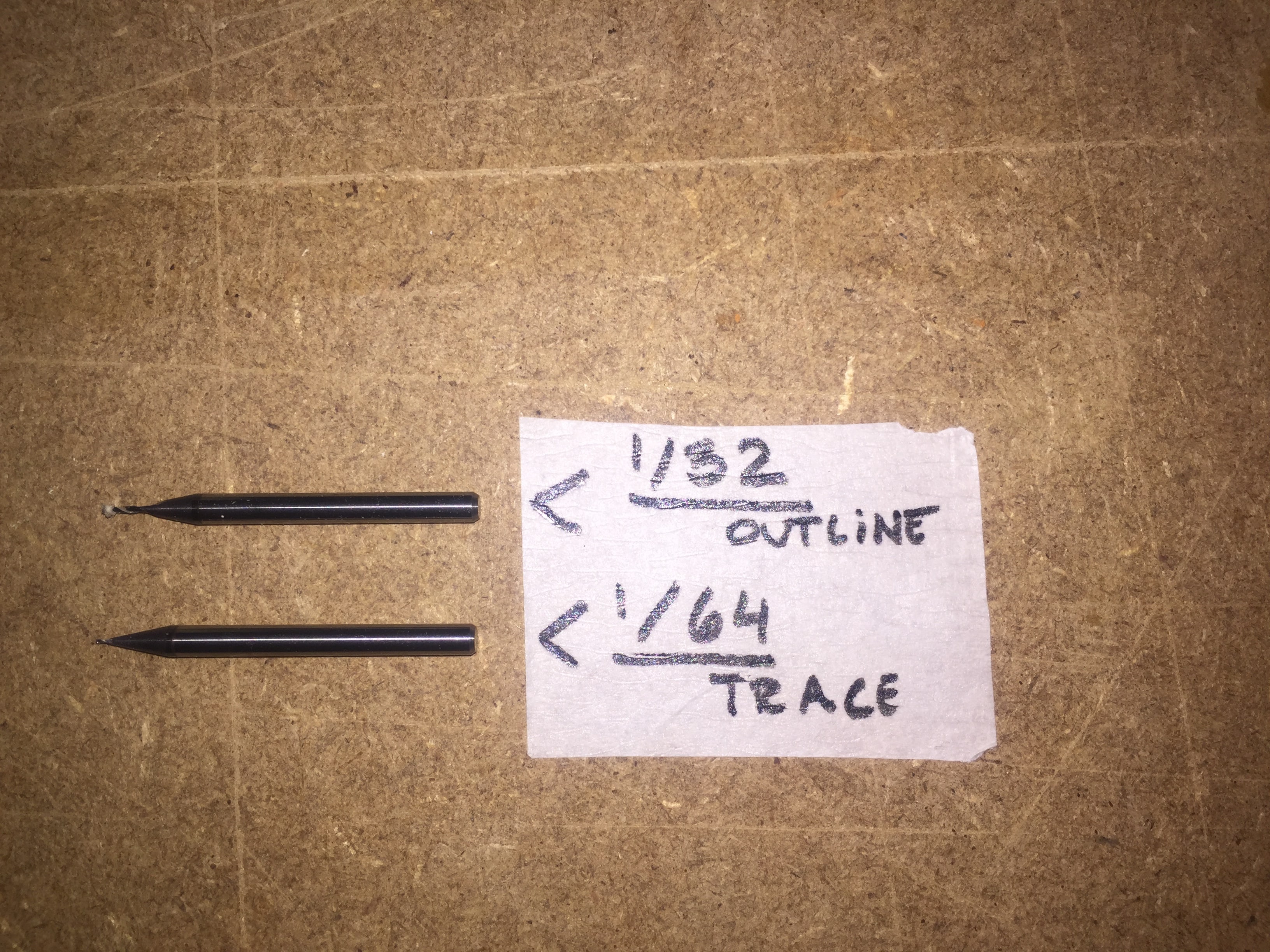
Milling Step 6
Router bits for trace and outline.
Milling Step 7
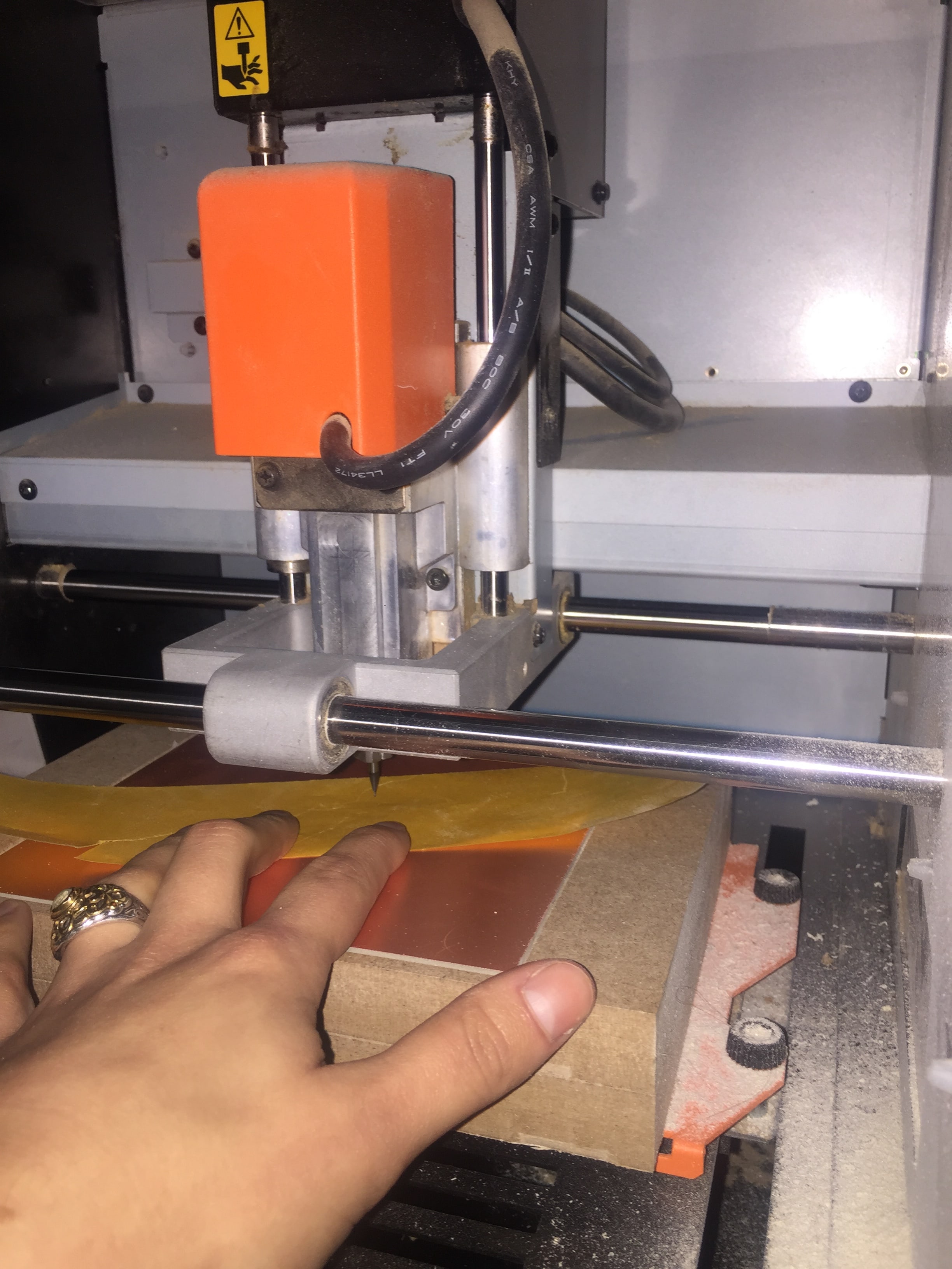
Set Z axis - Do 'paper test' by slowly lowering the router down onto the PCB board while holding a piece of paper just underneath and moving slightly side-to-side until the bit pierces the paper and firmly stops it from moving.
Milling Step 8
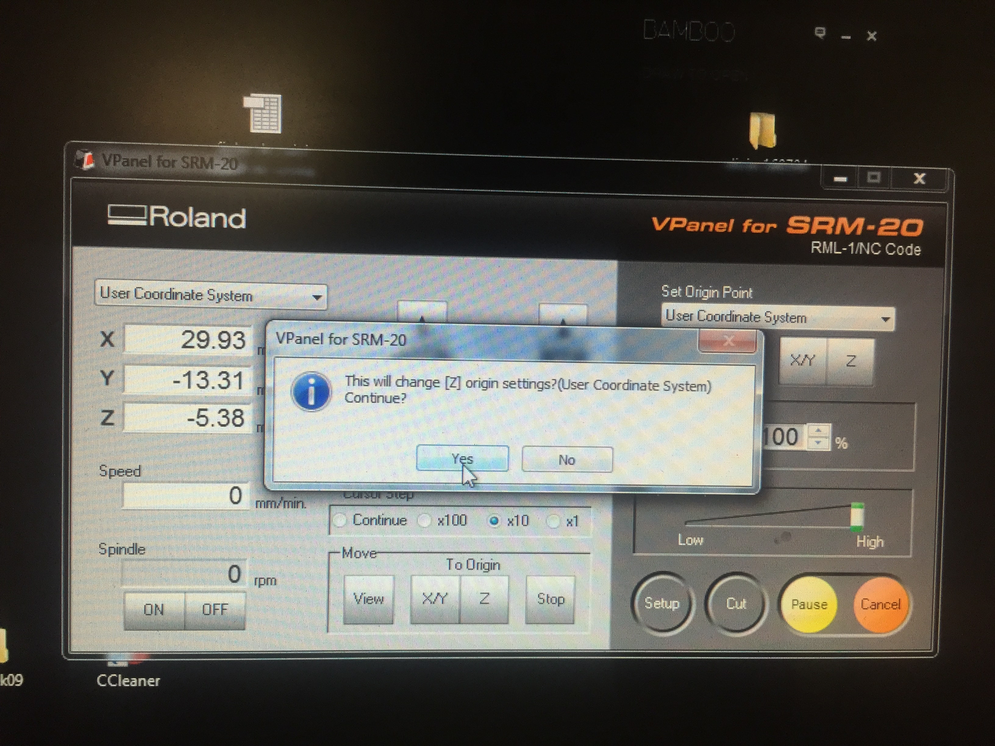
VPanel Set Z axis.
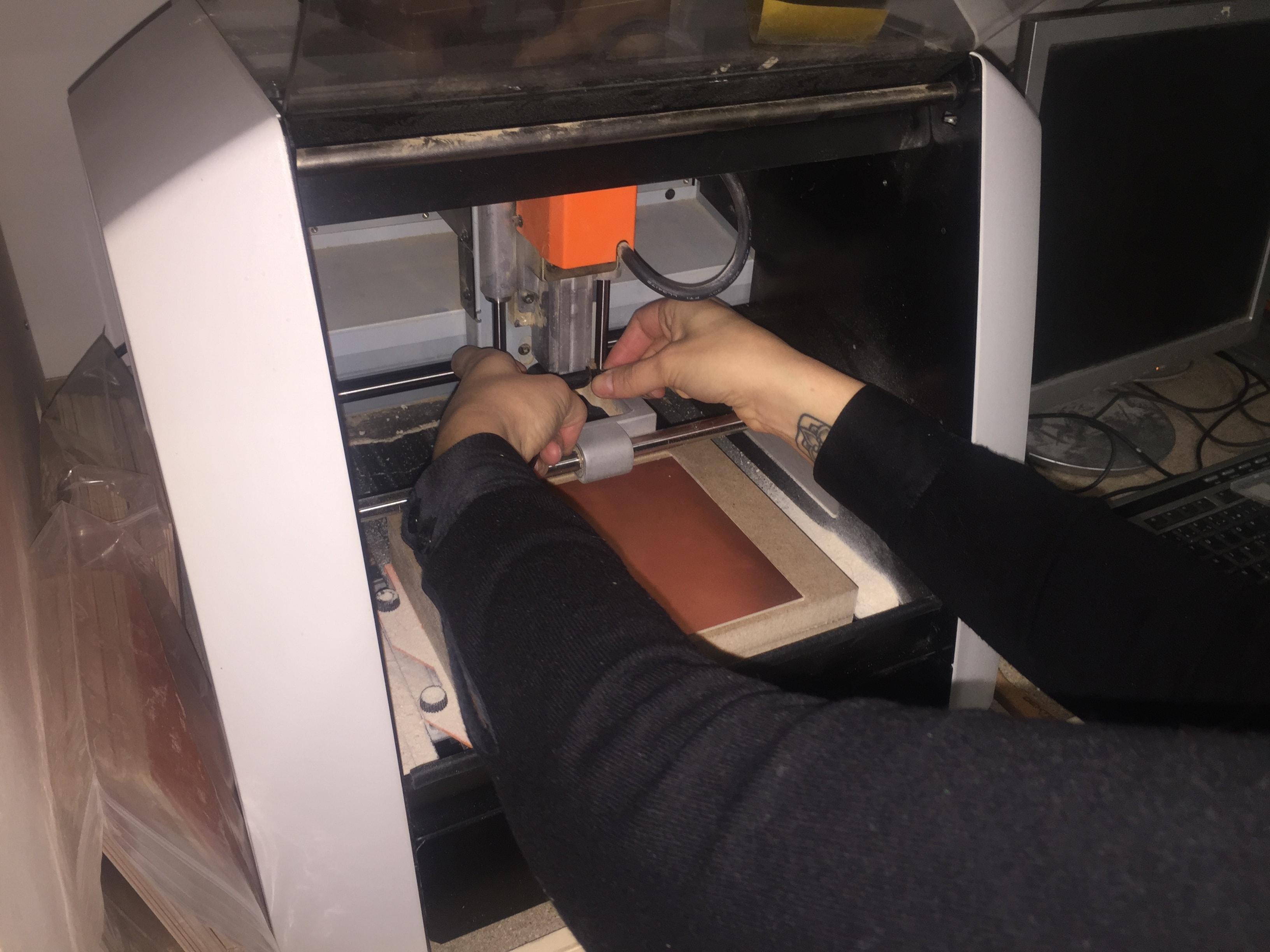
Milling Step 9
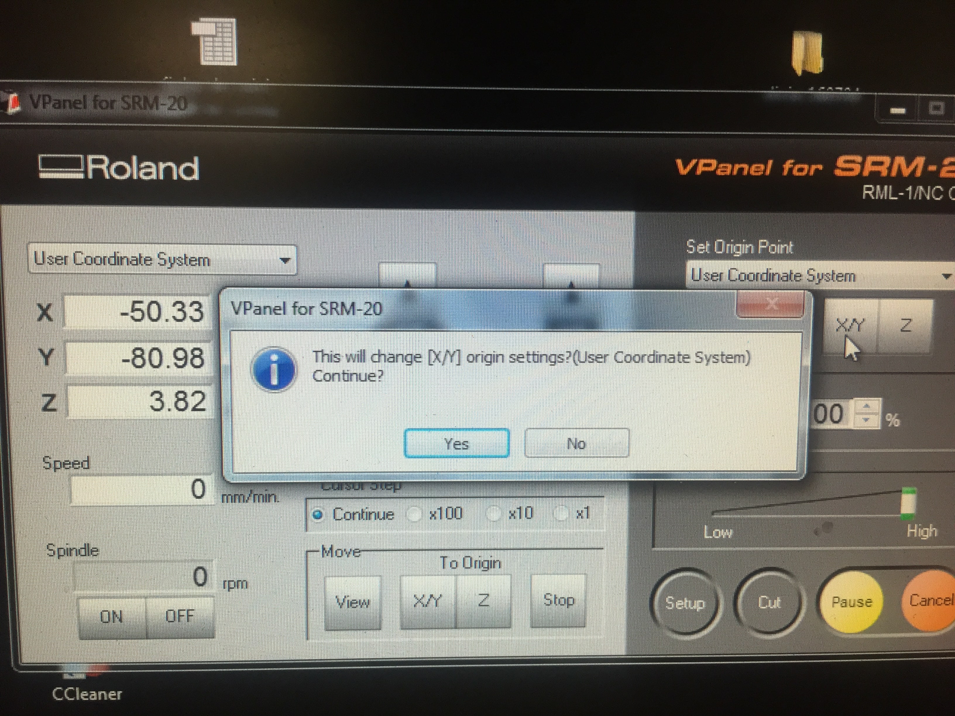
Set XY axis.
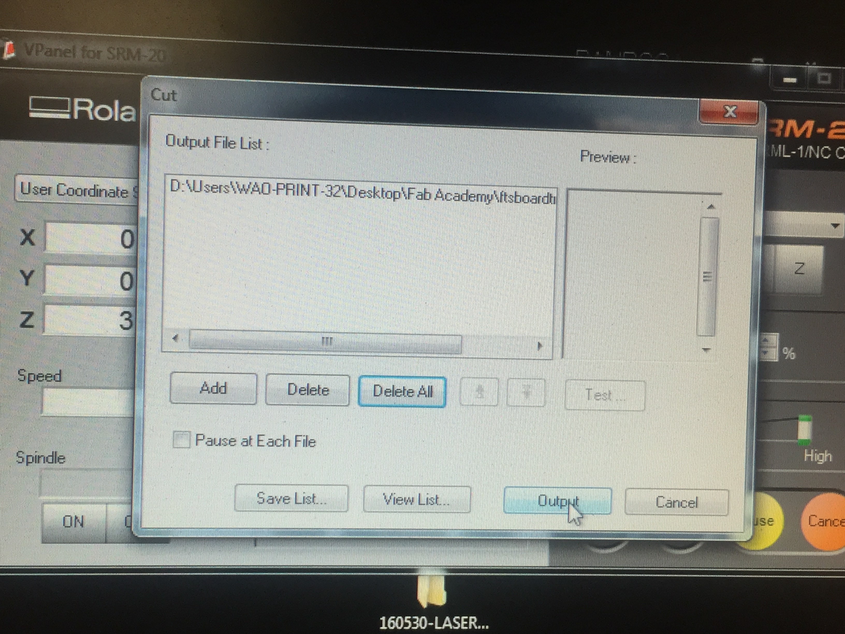
Milling Step 10
VPanel Set XY axis
Milling Step 11
VPanel Set XYZ axis
Milling Step 12
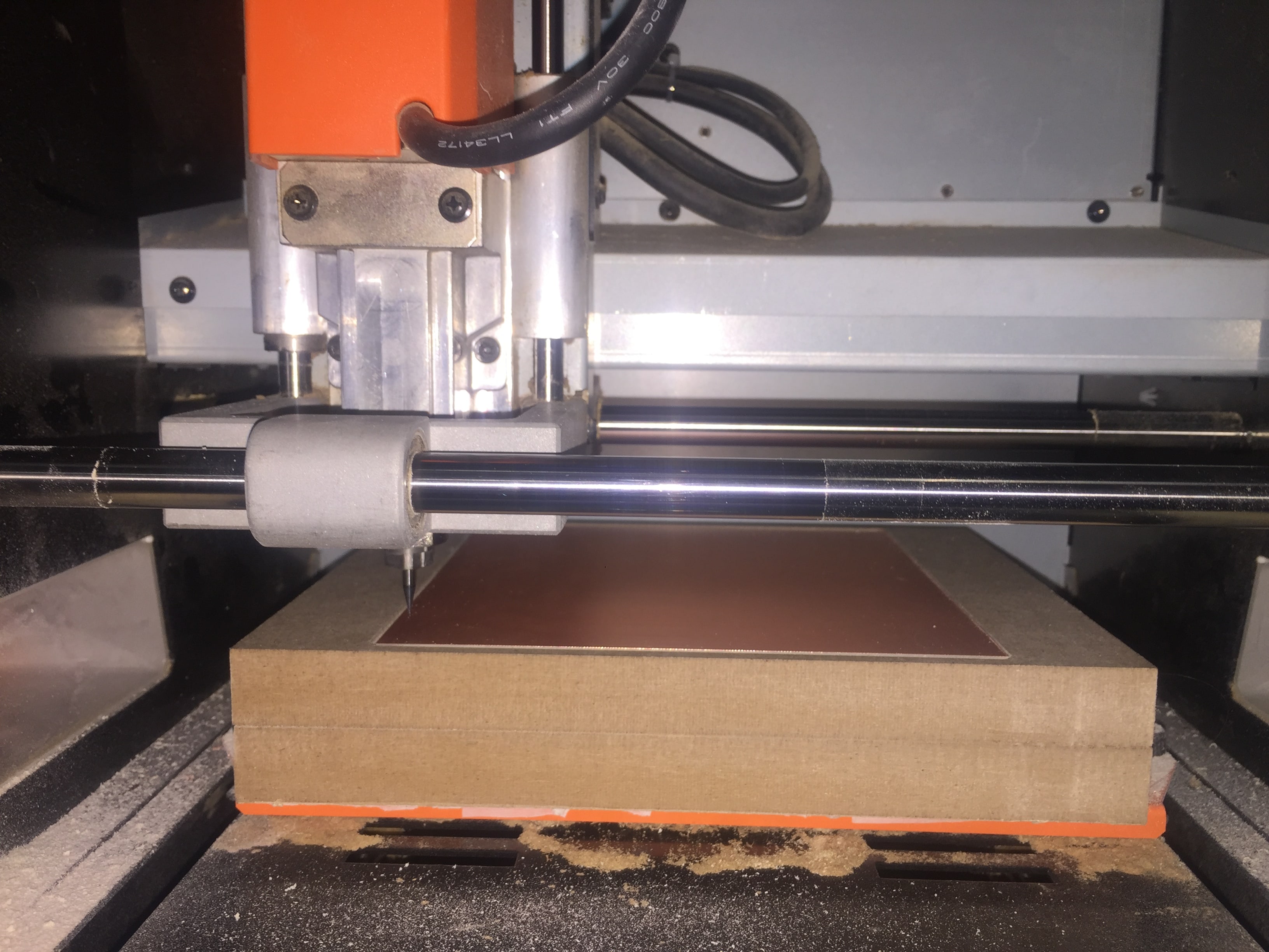
Close Machine cover
Milling Step 13
VPanel Select Cut
Milling Step 14
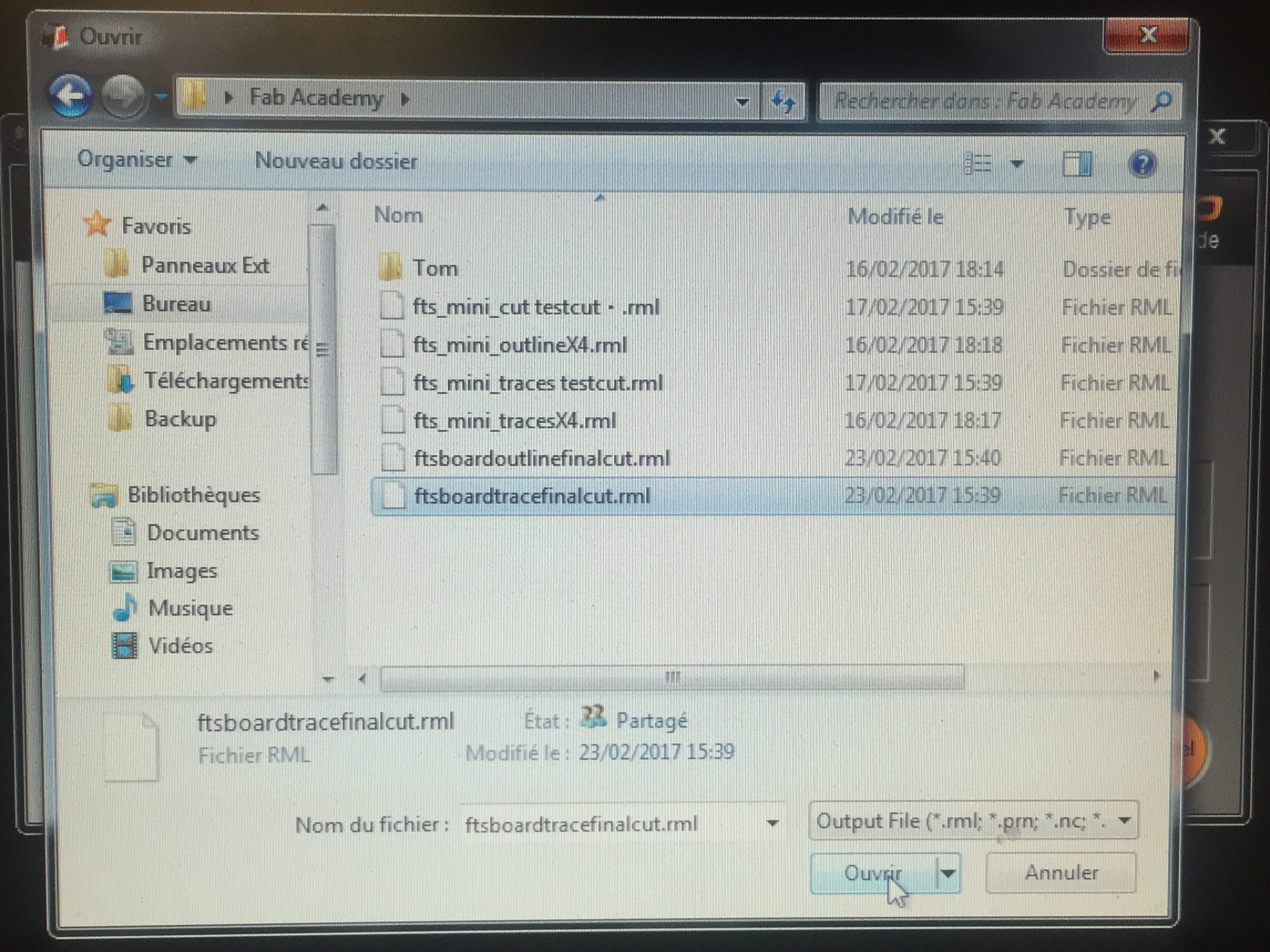
VPanel Select RML trace file first
Milling Step 15
VPanel Select Outprint to start milling job
Soldering
We used Brian's FabTinyISP tutorial and the schematic design as a guide to solder the electronic components to our circuit boards.
Electronics Components
| # | Component |
|---|---|
| 1 | 1x ATtiny45 or ATtiny85 |
| 2 | 2x 1kΩ resistors |
| 3 | 2x 499Ω resistors |
| 4 | 2x 49Ω resistors |
| 5 | 2x 3.3v zener diodes |
| 6 | 1x red LED |
| 7 | 1x green LED |
| 8 | 1x 100nF capacitor |
| 9 | 1x 2x3 pin header |
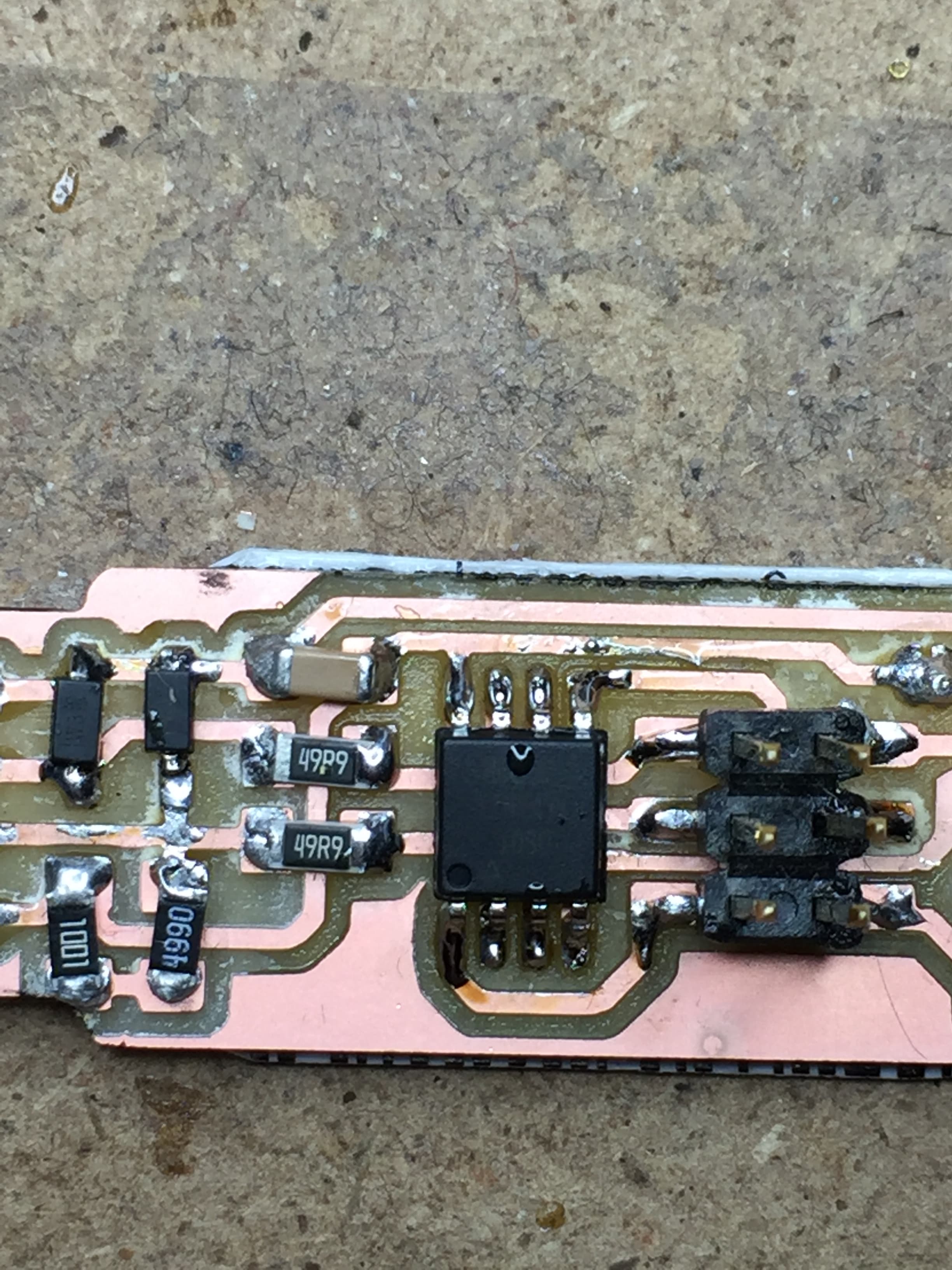
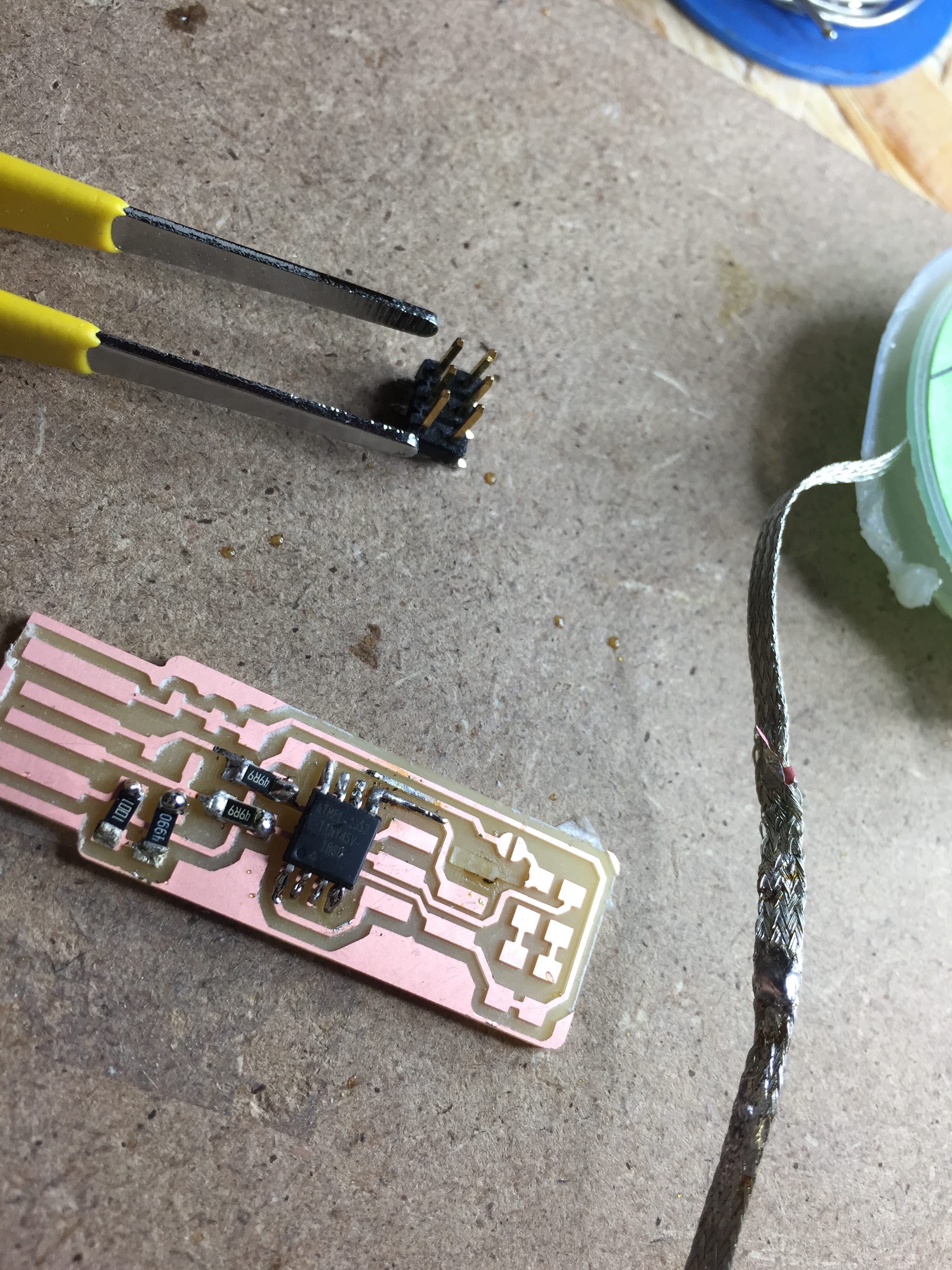
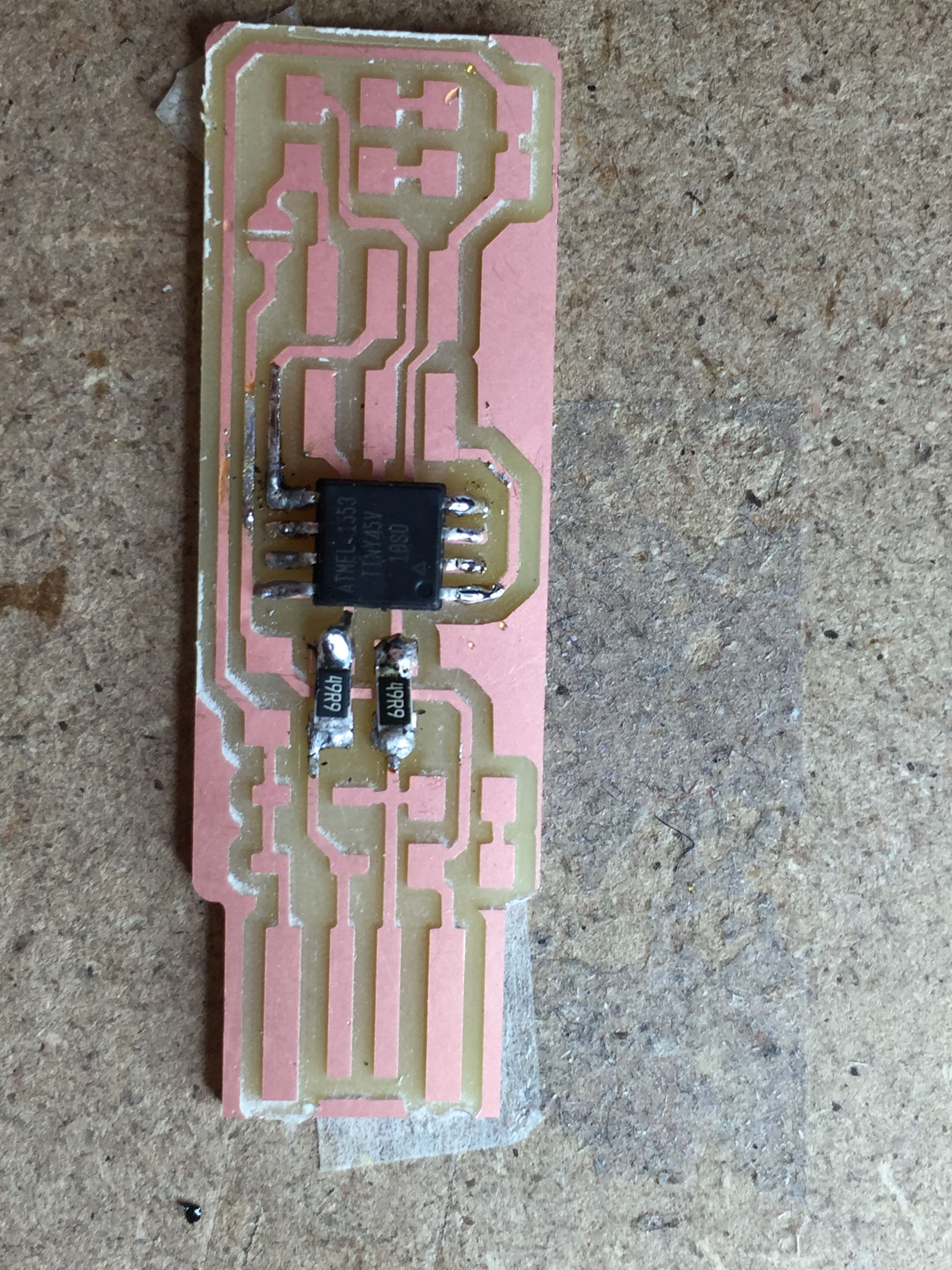
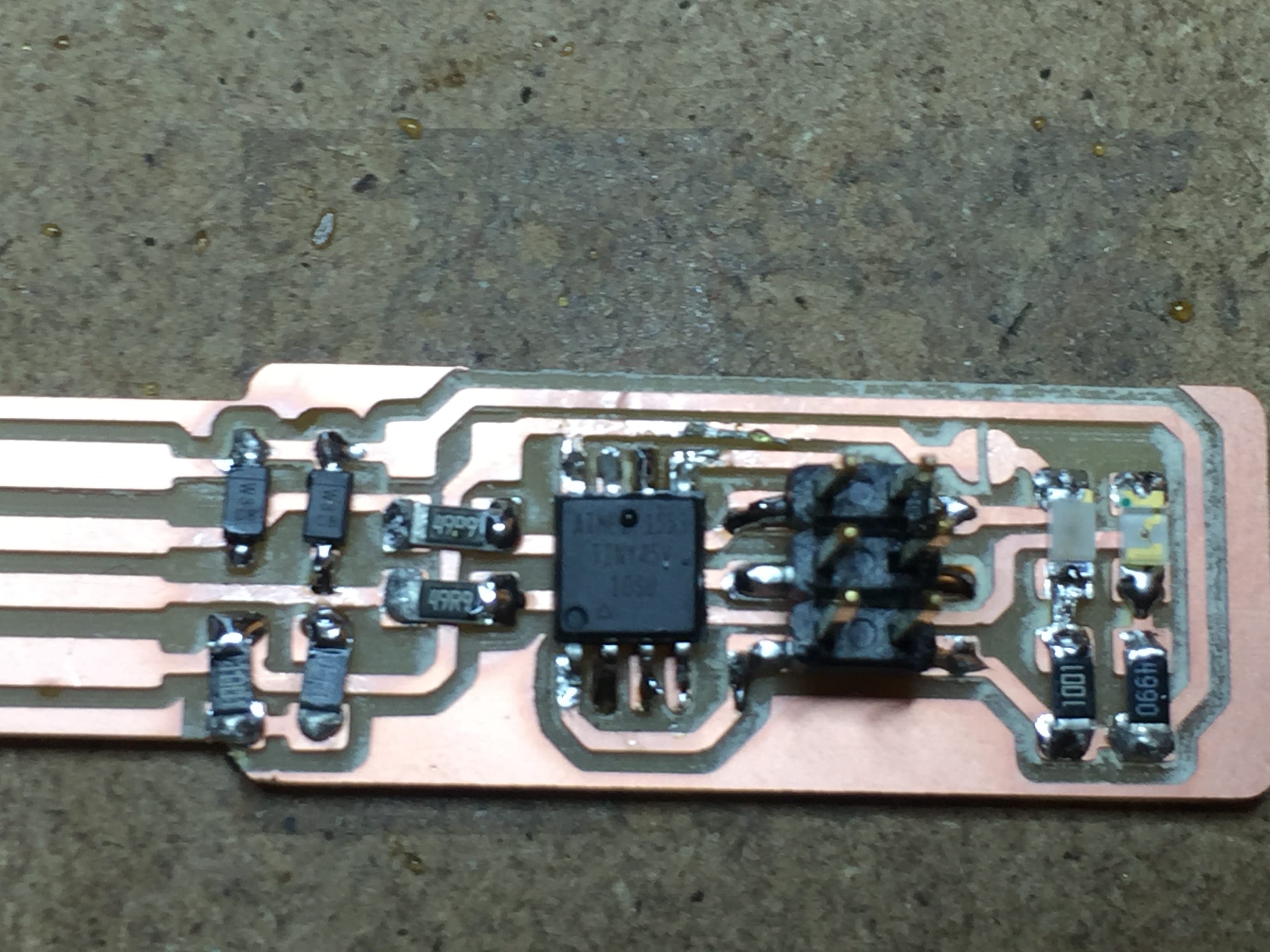
Soldering the Circuit Board with Electronic Components
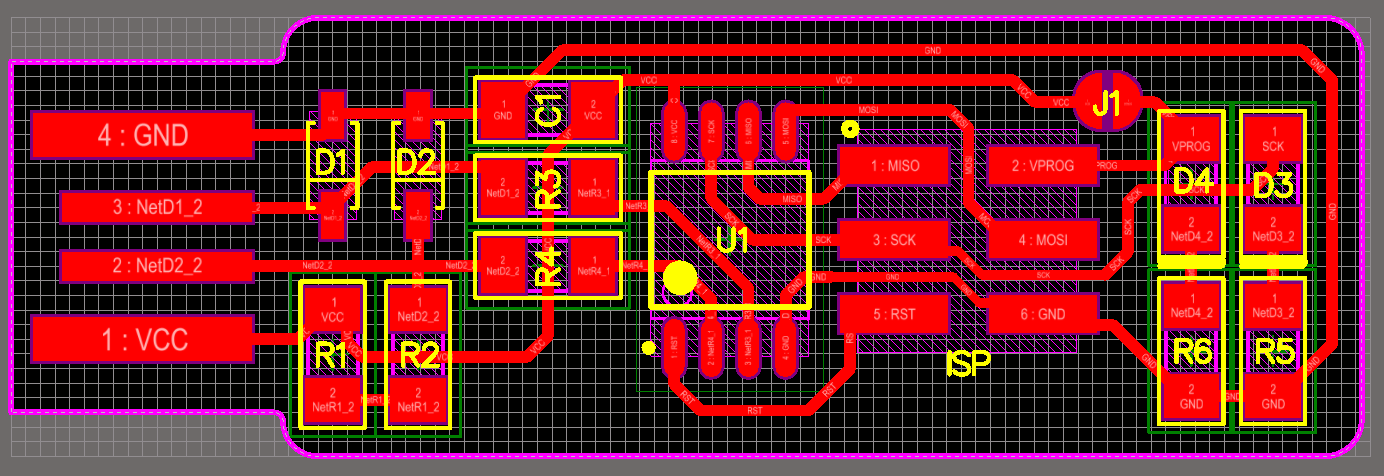
Circuit Board Schematic 1
Follow this schematic to understand where each component is placed.
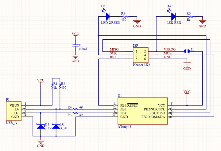
Circuit Board Schematic 2
Follow this schematic to determine the direction of certain component's positive / negative ends based on the flow of current.
Washing board with soap and water
Before beginning to solder, make sure to wash the circuit board with soap and water to get rid of any oil from your hands. This will lengthen the life of your board since oil can break down the copper traces over time.
Trial 1: Soldering Error: Braid ripping up copper
I ruined my first board when I used the braid to remove some extra solder, since there was not enough solder for the wire to remove and it melted into the copper trace instead. Beware!
Trial 2: First few solders
I ruined my second board because it was difficult to solder the Atiny 45 without also deposting solder between the nearby traces, thereby mistakenly creating a short.
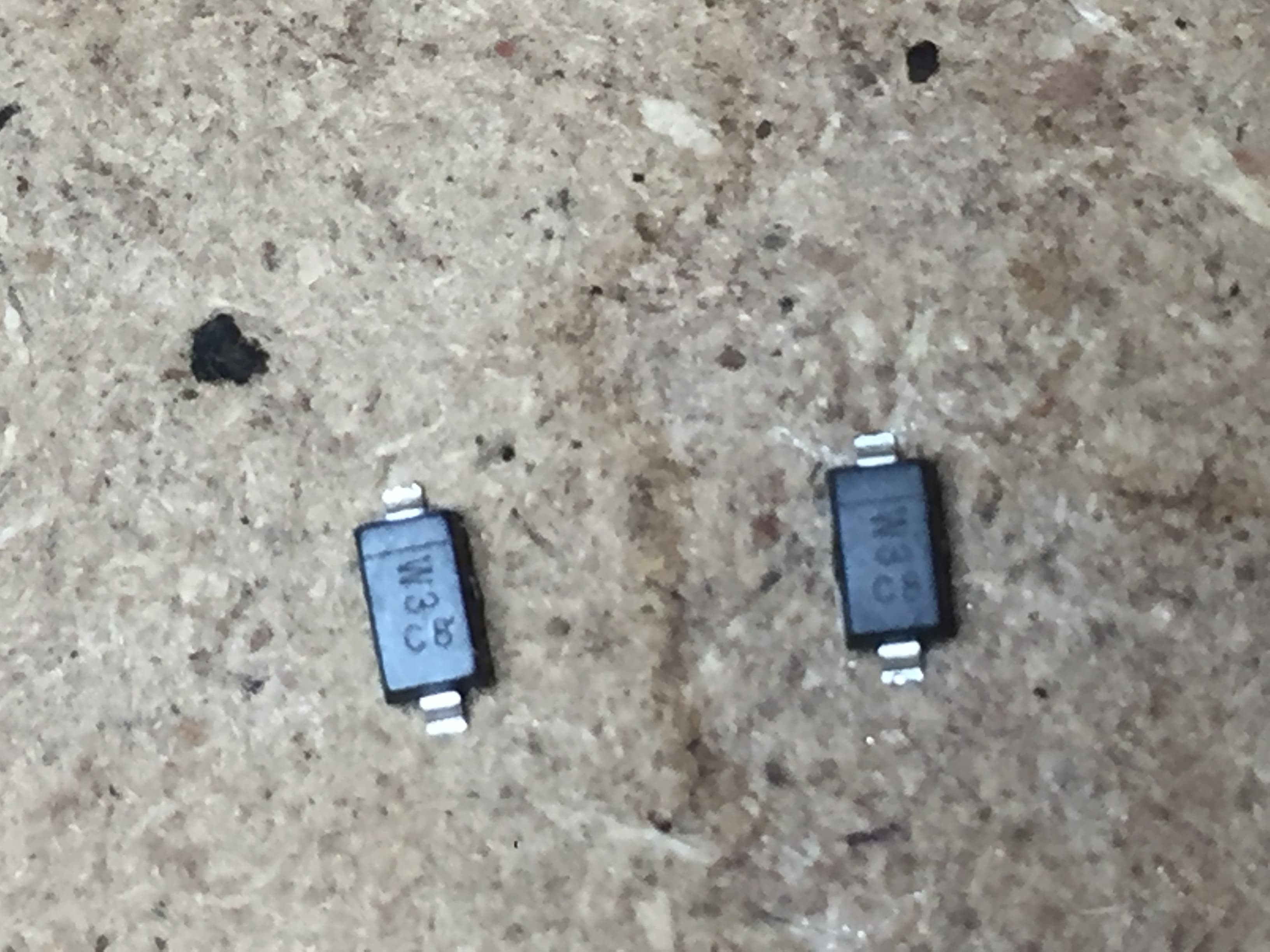
Trial 3: Soldering Error- Diodes/ LEDs + /- ends in wrong direction
My third board looked okay, until I realized I read the schematic in correctly and the LEDs and Zener Diodes were placed in the opposite positive/ negative directions.
Note: Zener Diodes Up Close – Line denotes negative end!
I removed the Zener Diodes and LEDs to inspect more closely for signs of their positive / negative ends. For the Zener Diodes the line denotes the negative end.
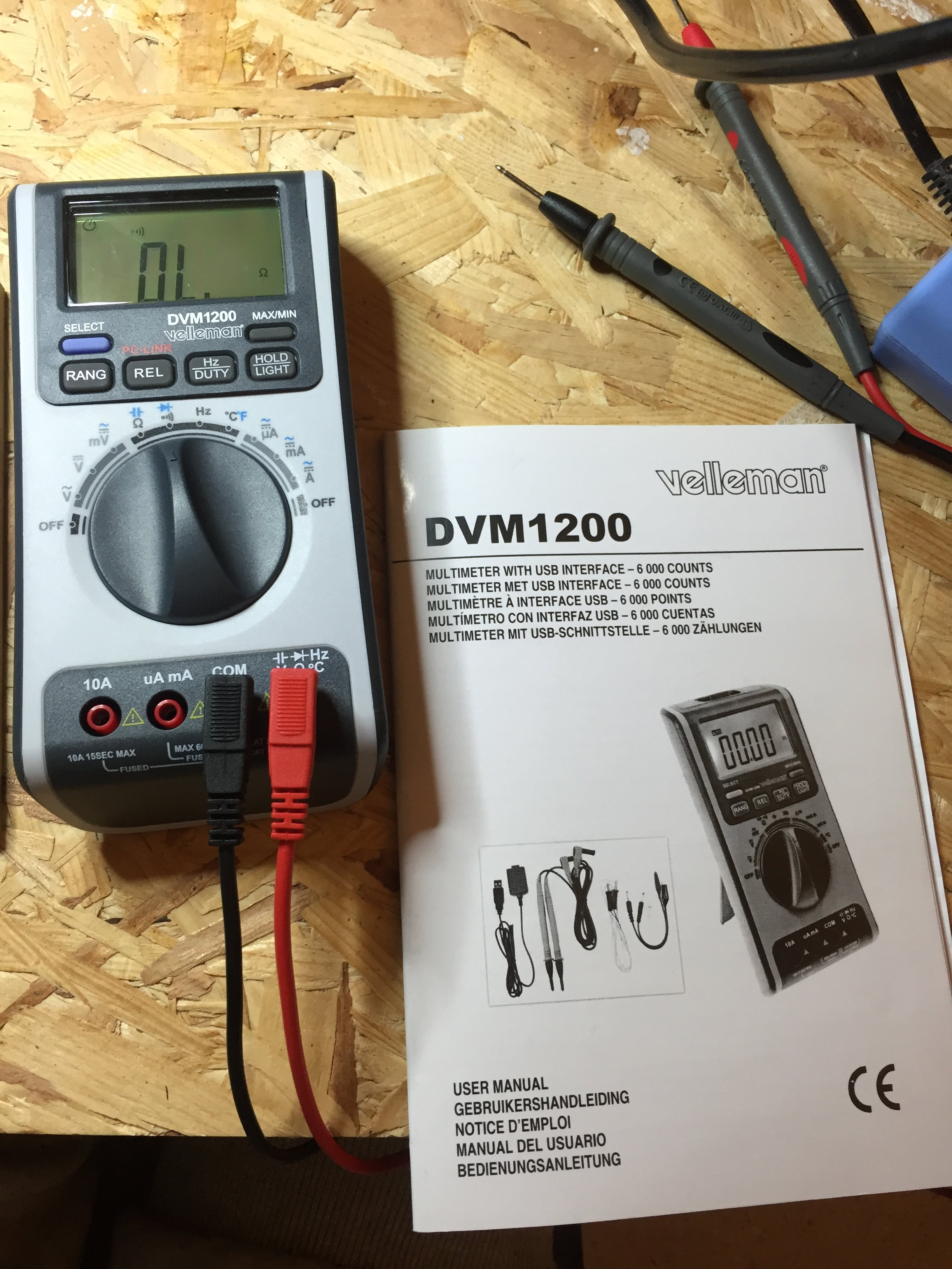
Note: Setting up Multimeter 1
I also tested the zener diodes with a Velleman DVM 1200 multimeter to understand which end was positive / negative. To set up the Multimeter you need to switch it on to the "audible continuity" symbol.
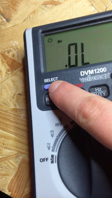
Note: Testing Diodes- Setting up Multimeter 2
Next, you need to press the blue "select" button to switch to the "diode" measuring mode.

Note: Testing Diodes- Setting up Multimeter 3
You will know that the multimeter is set up correctly when the diode symbol appears on the screen where the "audible continuity" symbol once appeared.
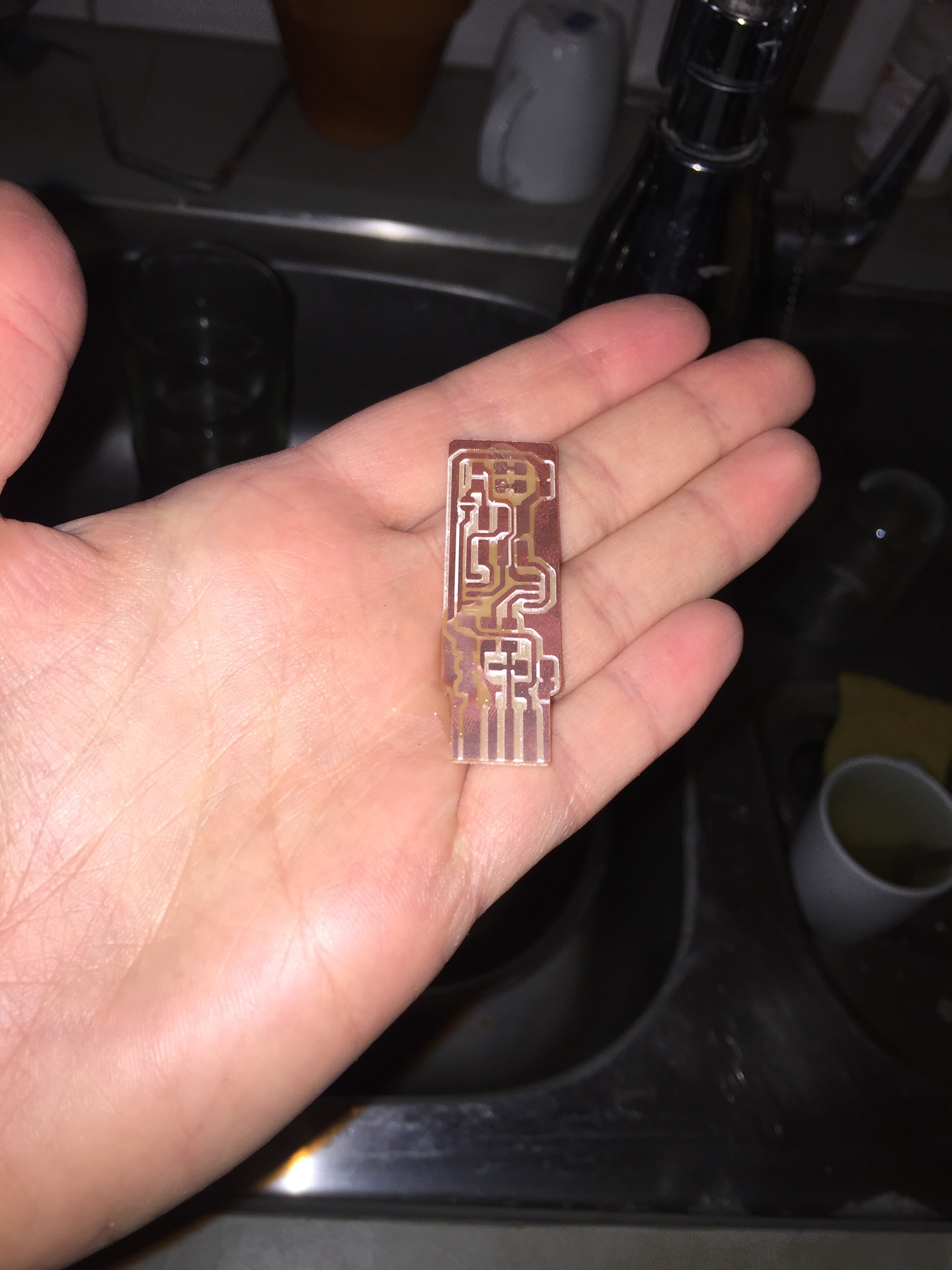
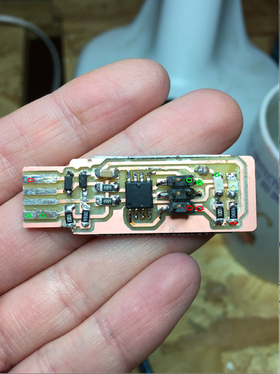
Trial 3: Finished Re-soldered board – Diodes/ LEDs in right direction
I re-soldered the zener diodes and LEDs in the correct direction, and finally had my first finished board!
Programming
I attempted to program the board using the Git Terminal, AVRDude, and the firmware downloaded to program our board, but was unsuccessful in the end. Roman attempted to program the board remotely as well, but also could not.
Git Commands to Program Circuit Board
| Step # | Command |
|---|---|
| 1 | make clean |
| 2 | make hex |
| 3 | make fuse |
| 4 | make program |
Attempting to program board
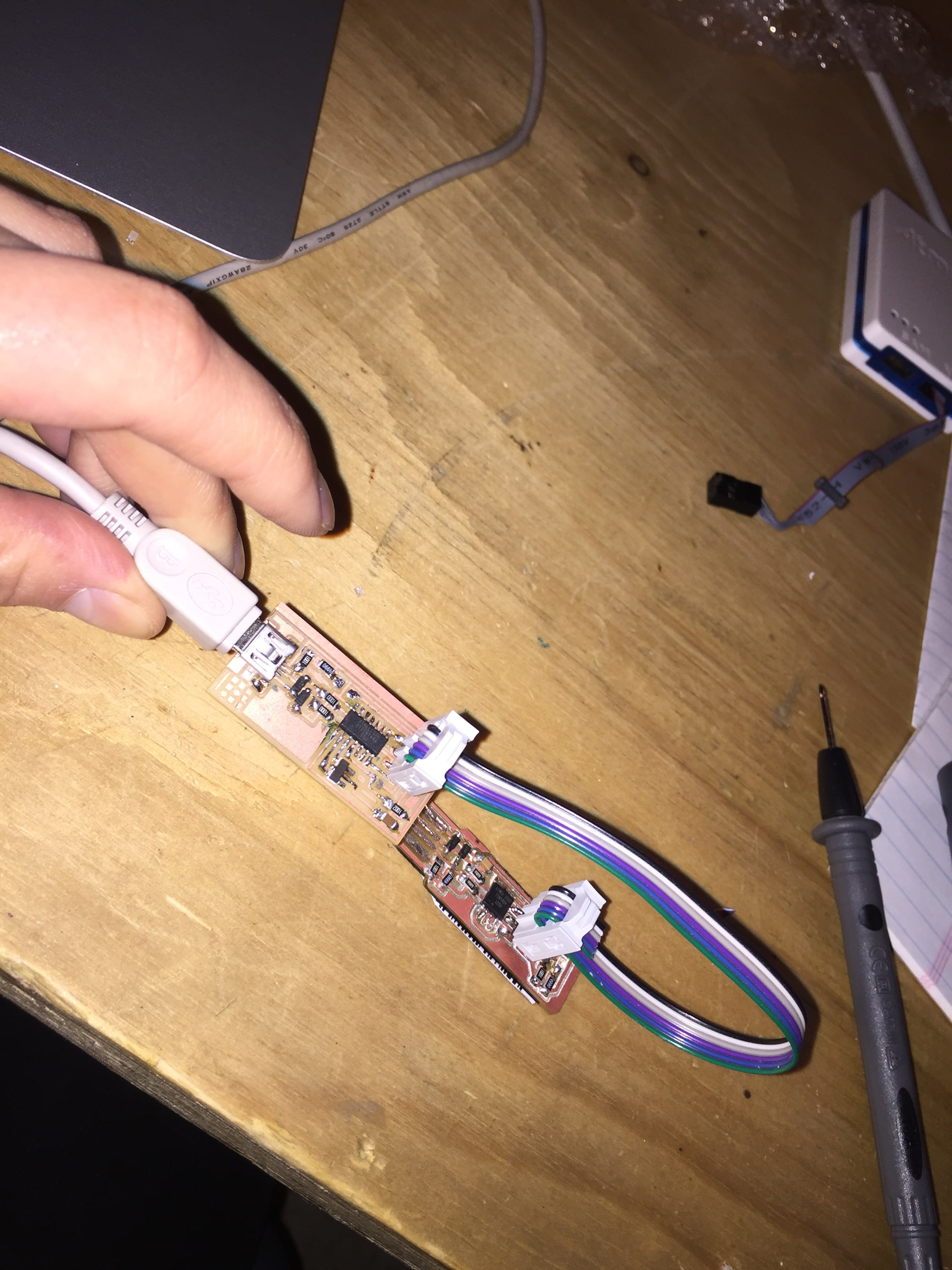
I followed the steps to download the necessary firmware and connect my circuit board to Thomas's programmer and then into my computer's USB drive. The red LED light of my board lit up, which was supposedly a good sign, however after two days of trial and error with Roman's help, we still could not program my board.
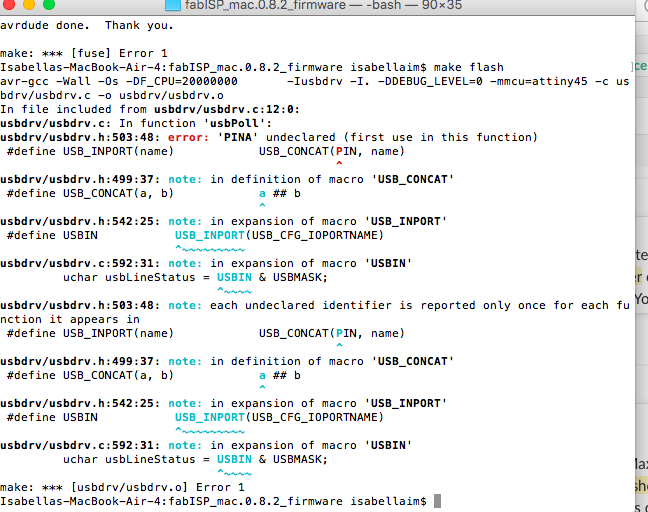
Programming- Terminal Output Error
This was the error that I continually got via the Git Terminal when running the final command "make fuse".
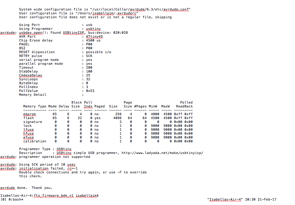
Programming- Terminal Output
This was the terminal output when Roman remotely tried to help program my board.
Troubleshooting
Roman then helped me troubleshoot what could be wrong with my board, the cable, or the programmer.
Troubleshooting - Cable Connection 1
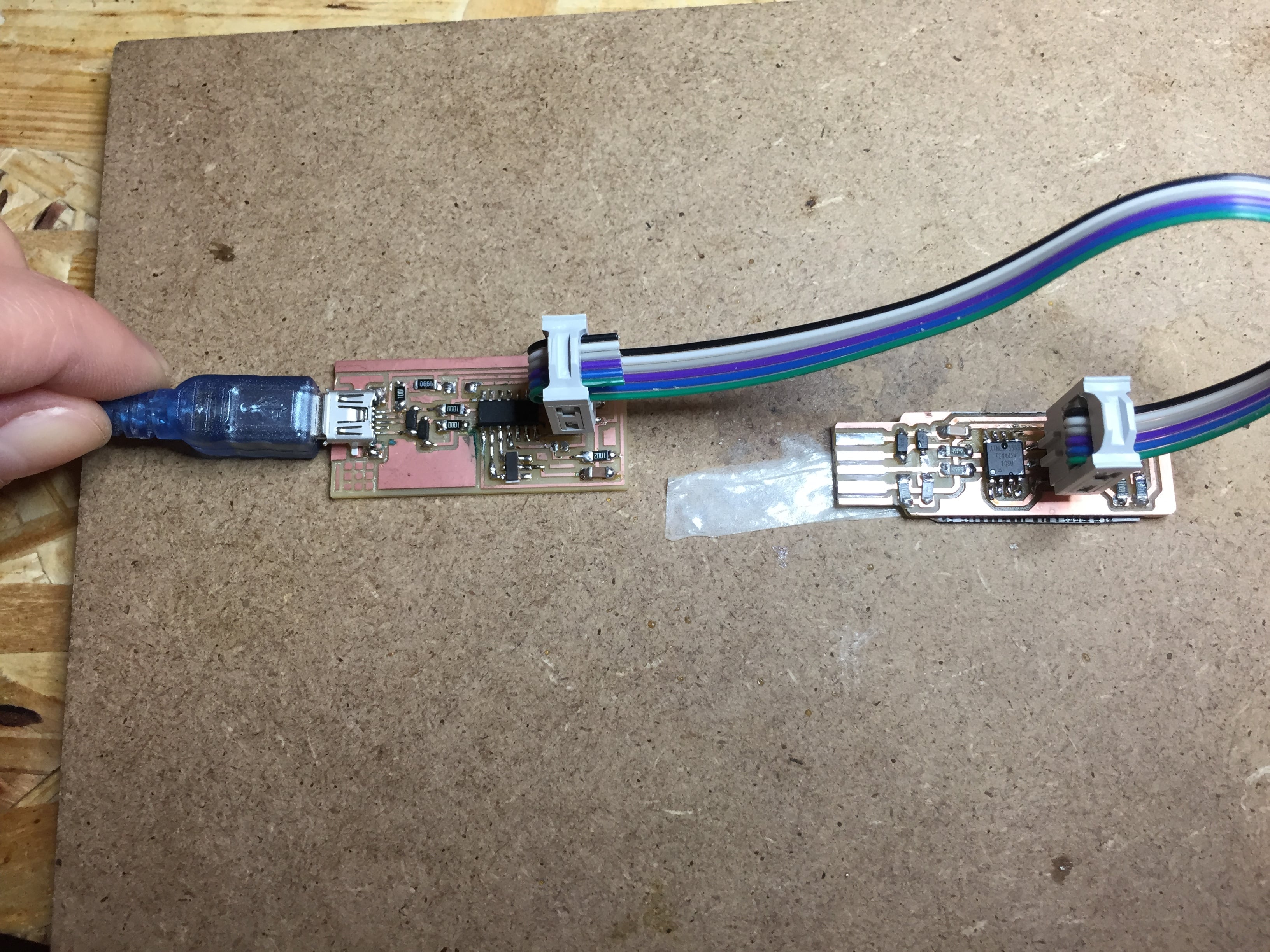
Troubleshooting - Cable Connection 2
Troubleshooting - Cable Connection 3
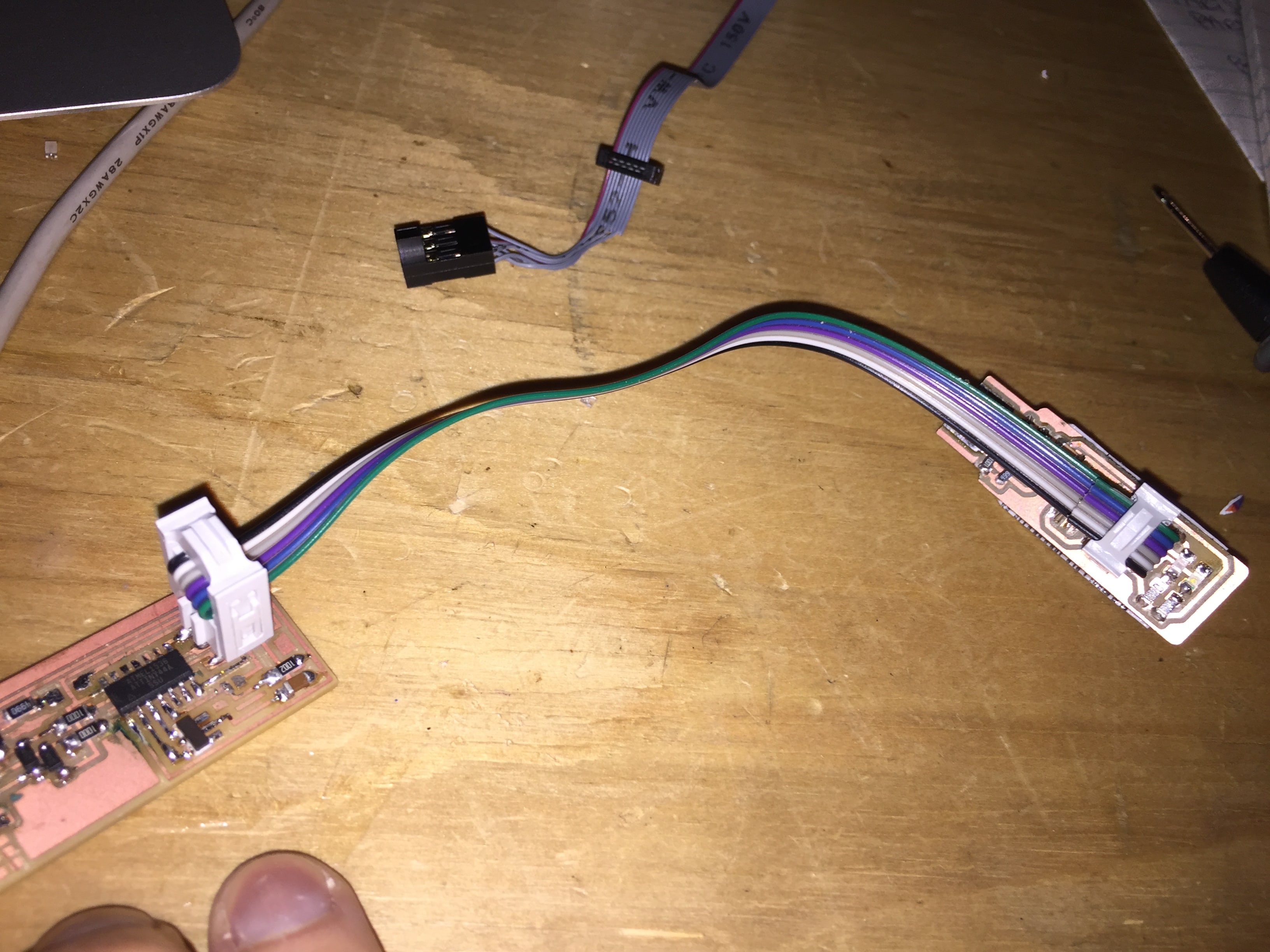
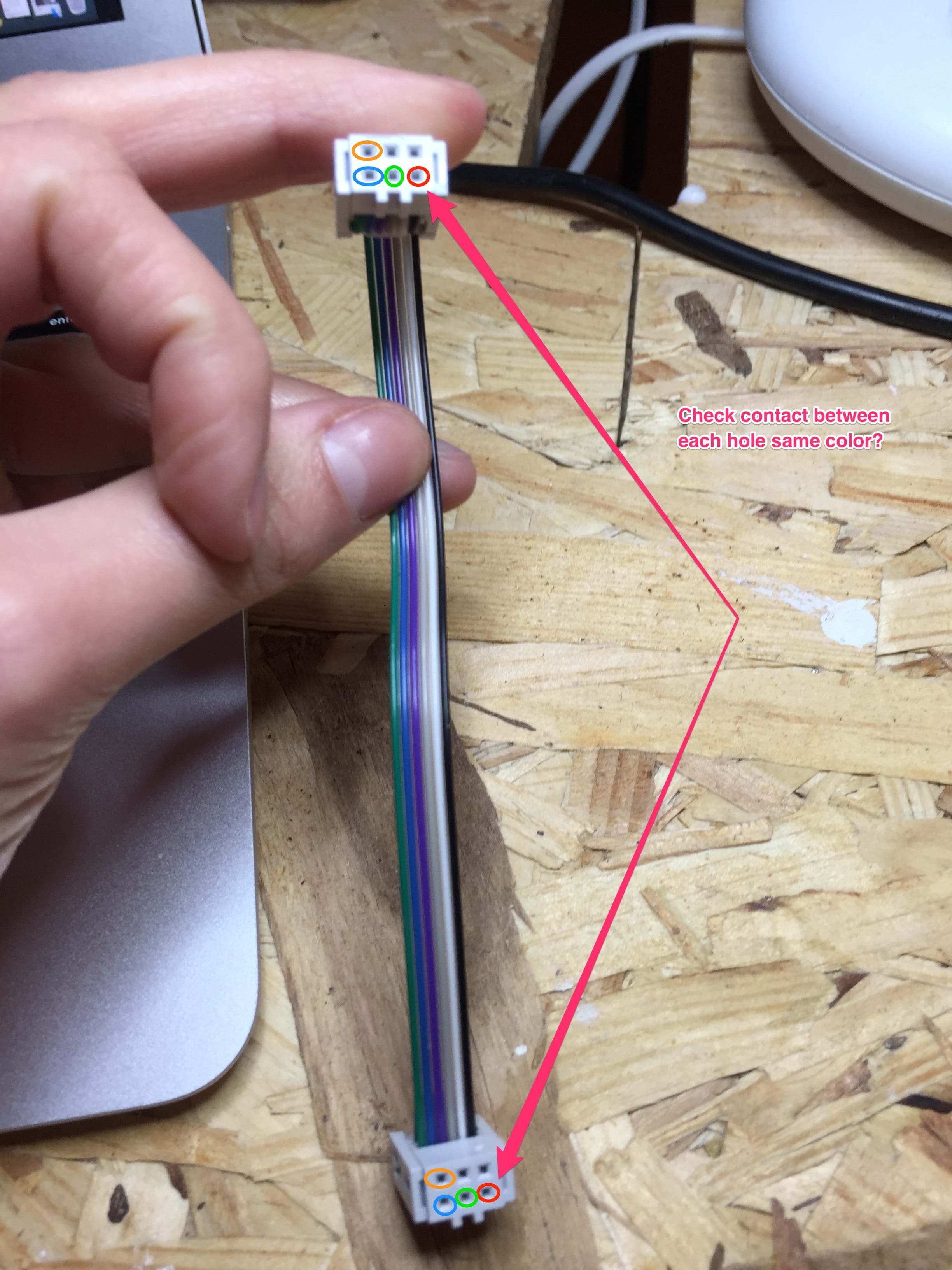
Troubleshooting- Testing connection in cable wires
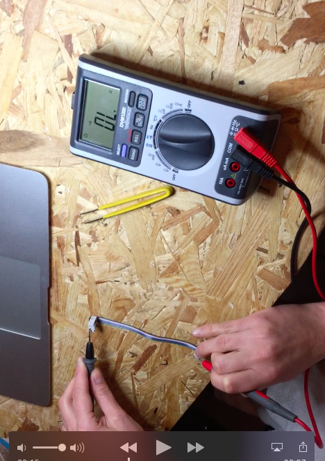
Troubleshooting- Testing connection of wires with multimeter 1
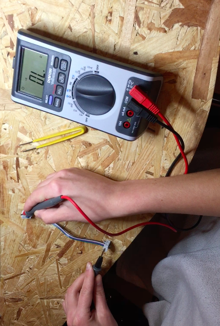
Troubleshooting- Testing connection of wires with multimeter 2
Troubleshooting-Testing resistances of LEDs/ Pin Header/ USB
Troubleshooting- Re-soldering Atiny