Week 6: Electronics design
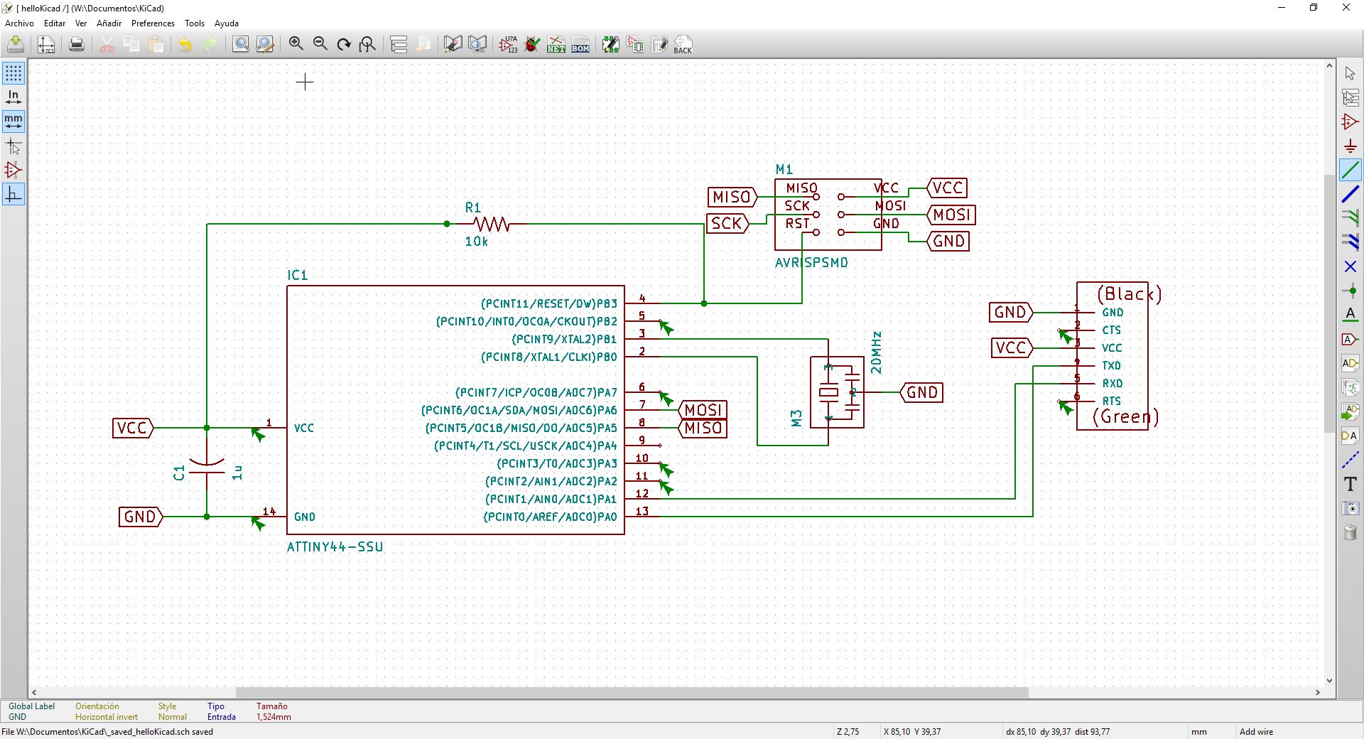
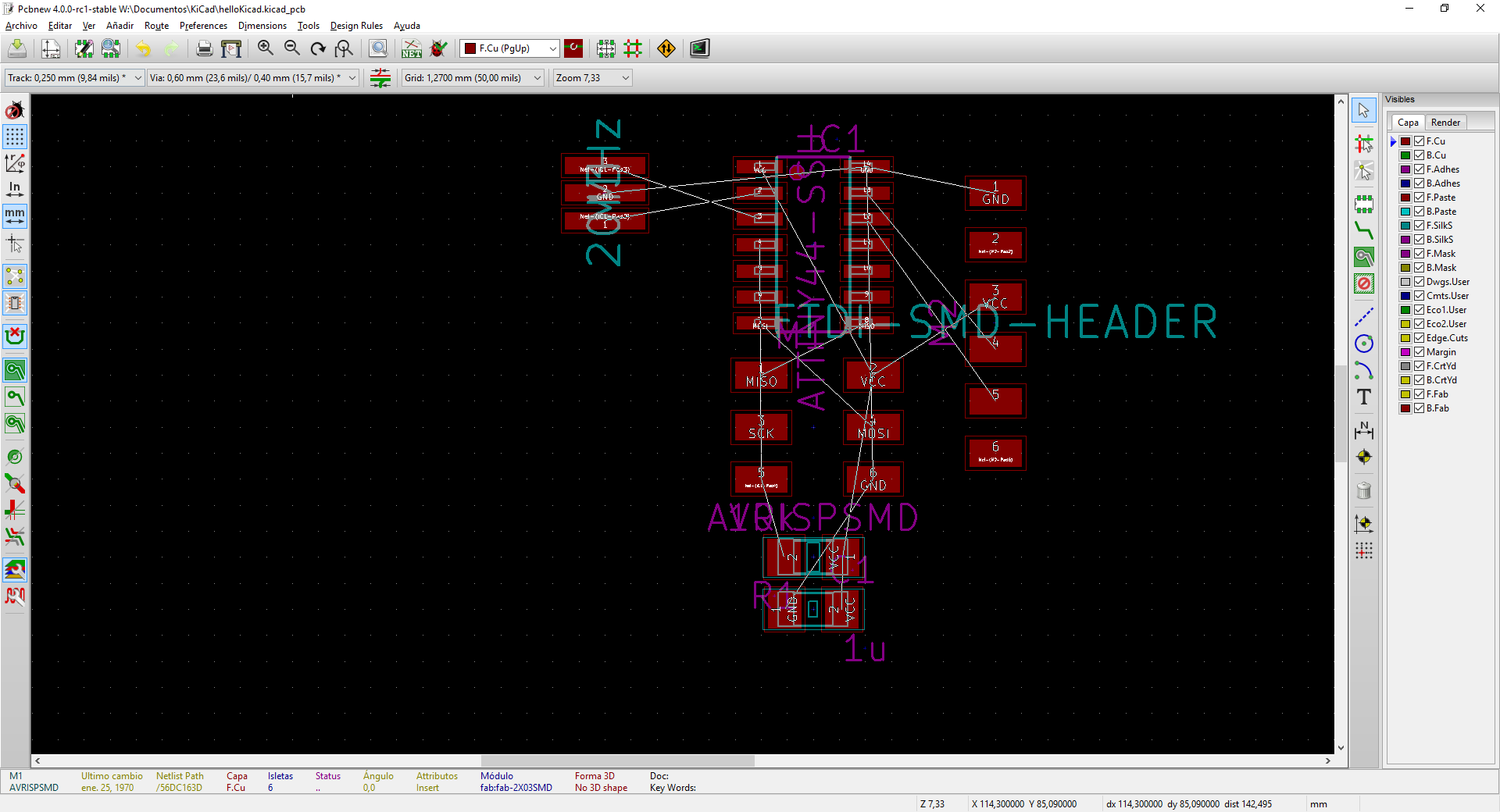
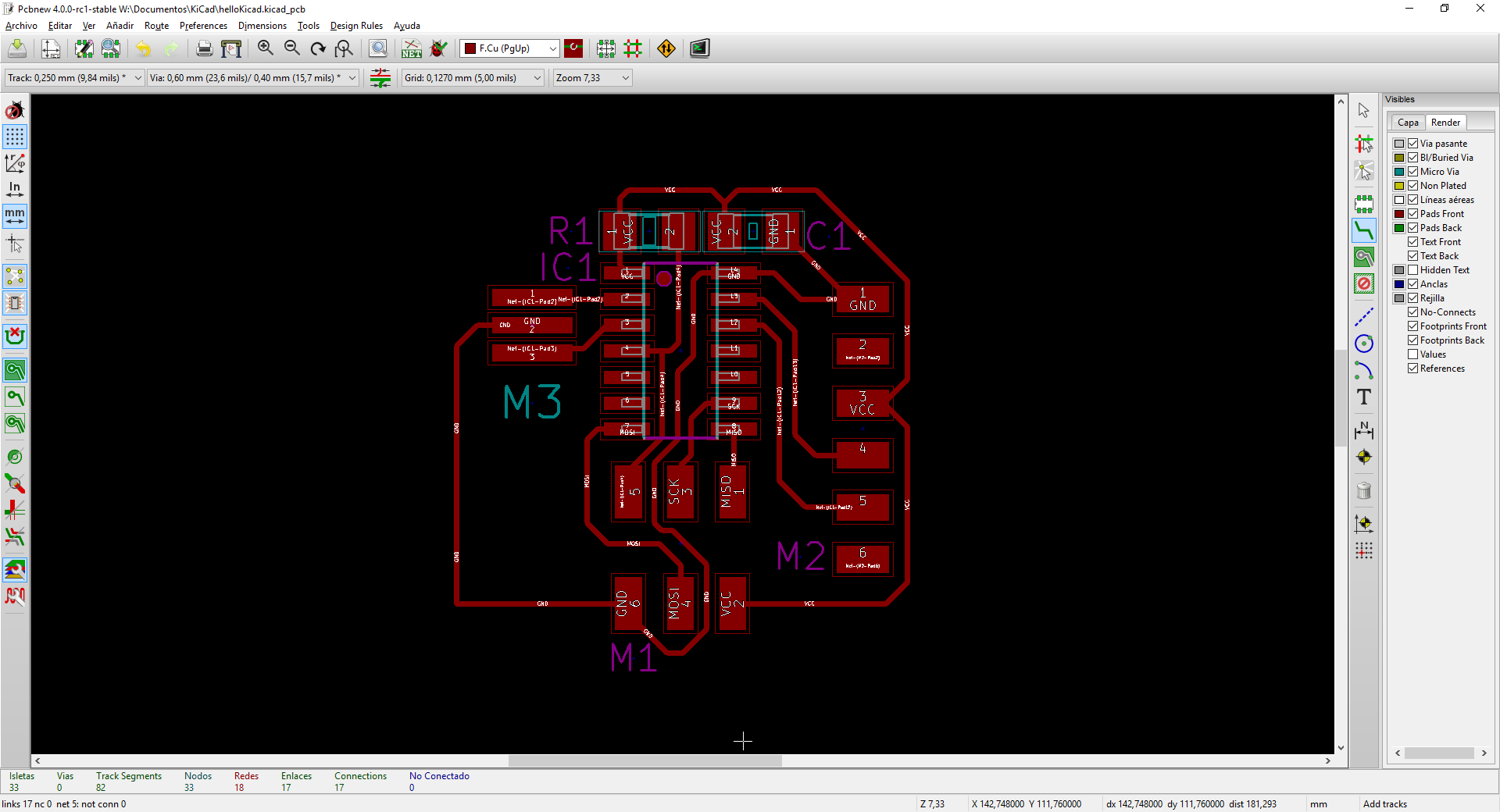
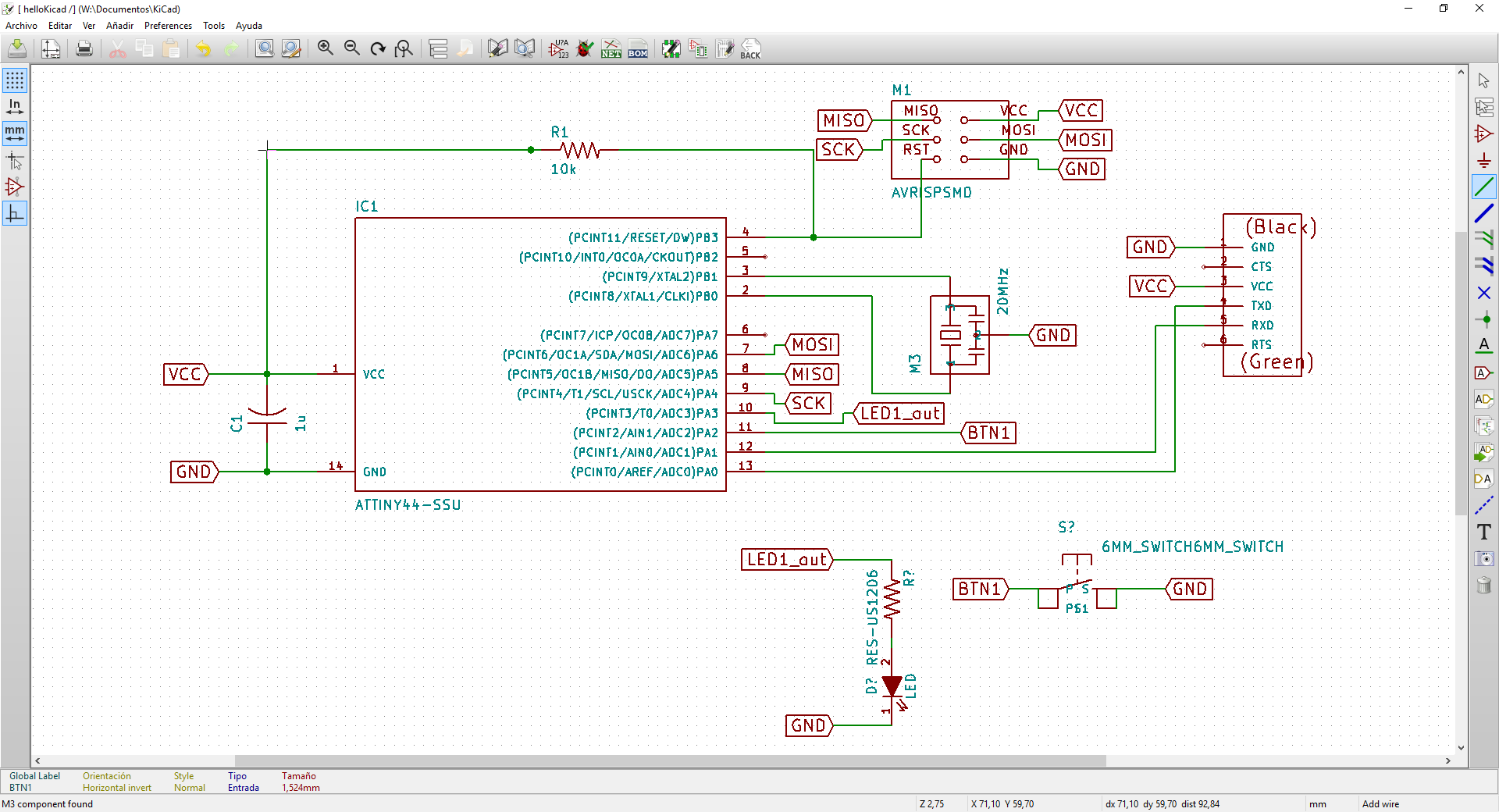
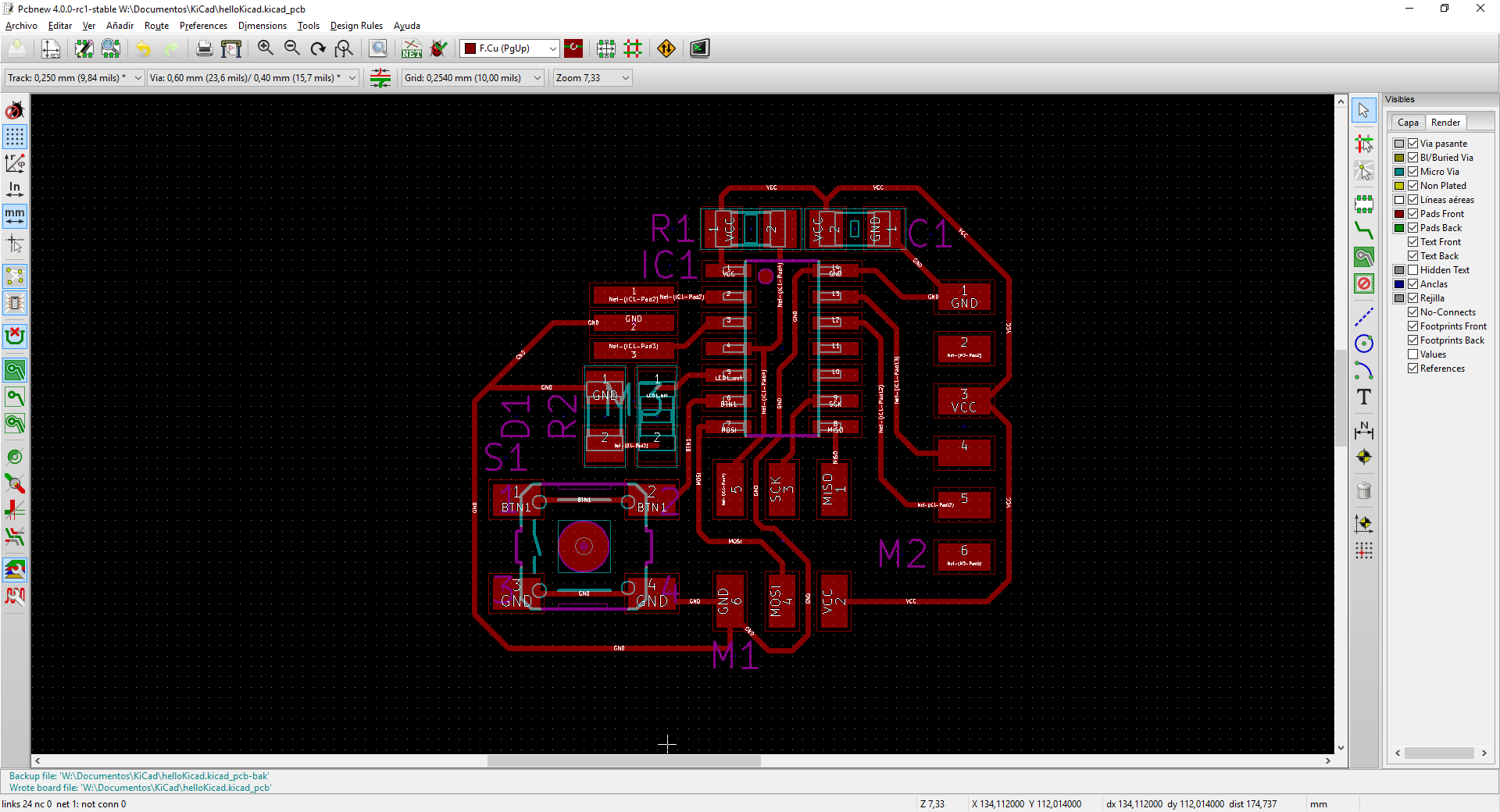
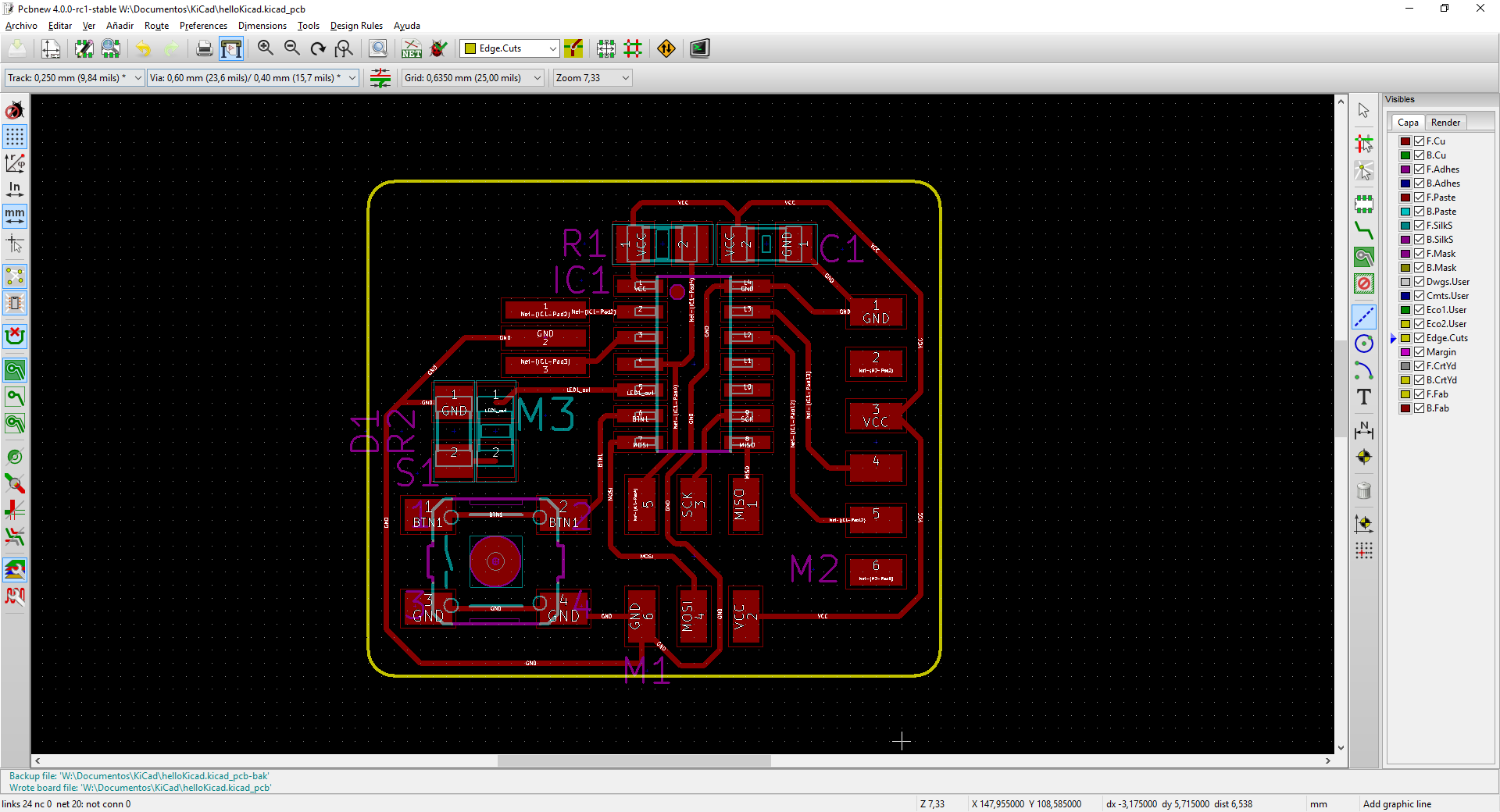
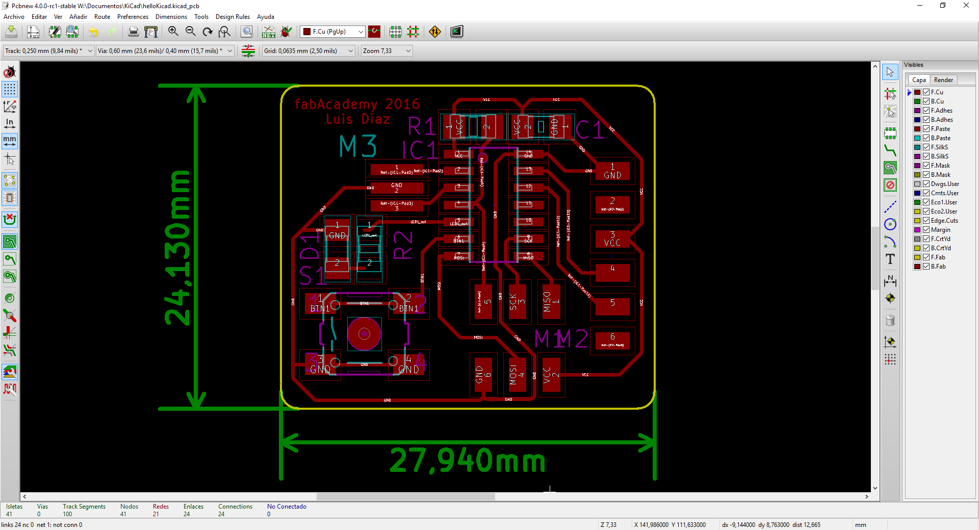
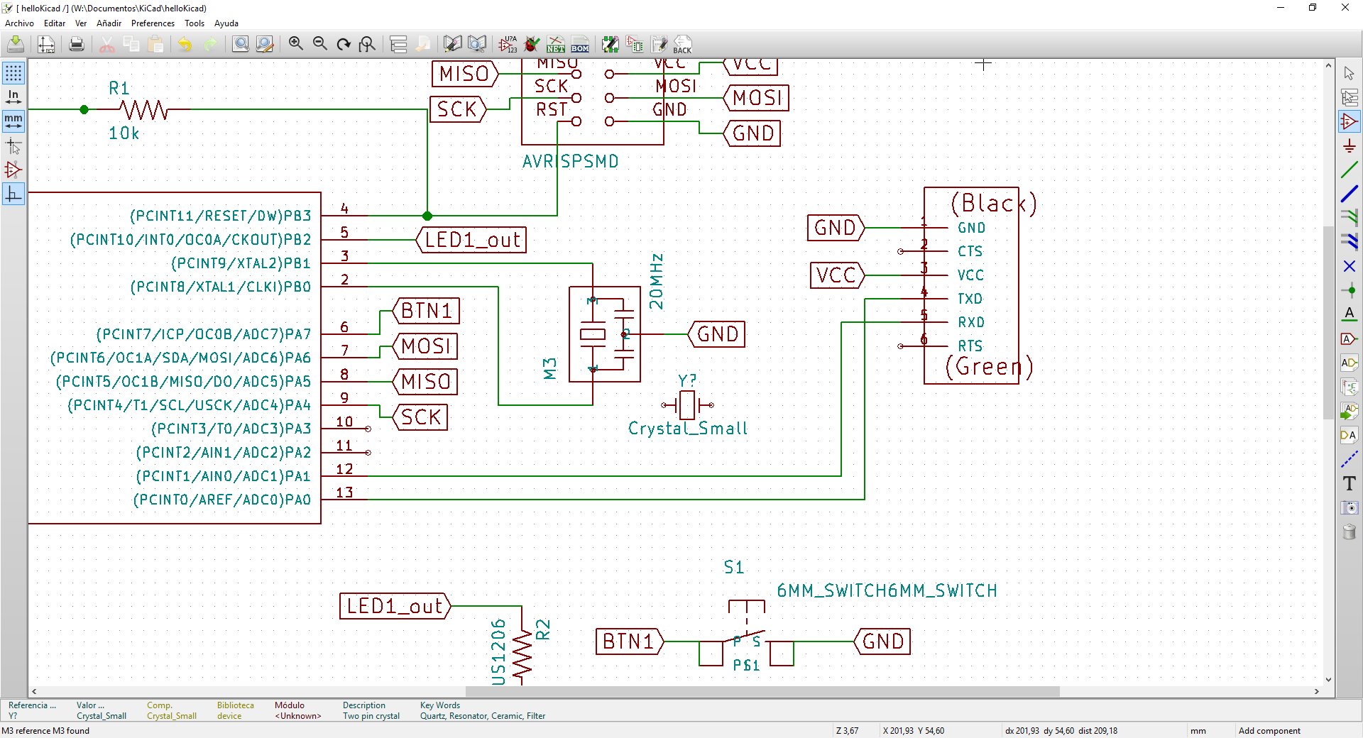
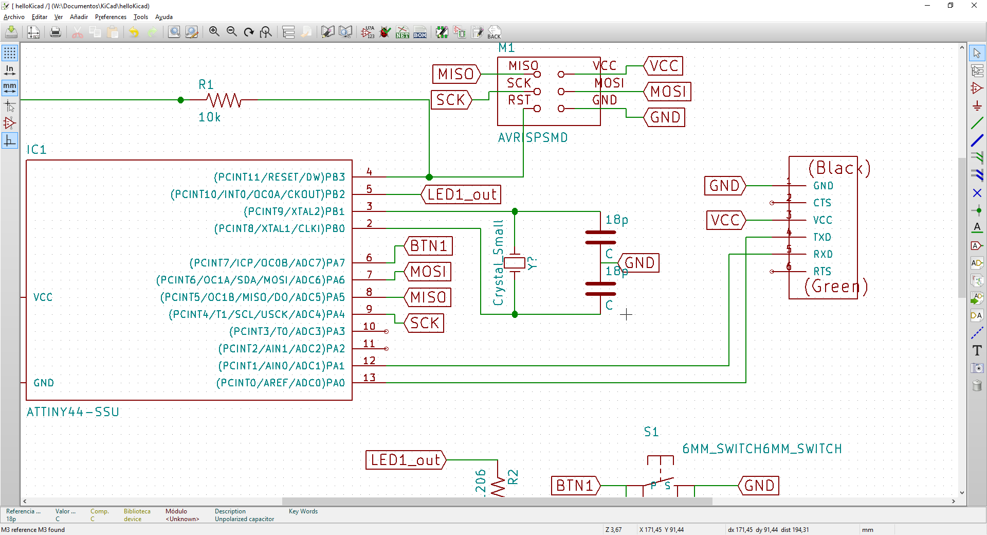
This is the first assignment I missed documenting on time because of the events occurred at fabLAB Asturias during March. Even though I have designed boards in the past it's been a long time since the last one, as usually David, my instructor, takes most of the electronic design at fabLAB. I have used OrCAD during the degree and my final project and then switched to free EAGLE when I didn't have access to OrCAD. But for this assignment I wanted to switch again and try KiCad. David has been using it for more than a year now and if he says it's amazing, it surely will. He started using it when we watched the Interactive routing video. It was very convenient that Anders posted a library for the fab inventory, thanks Anders!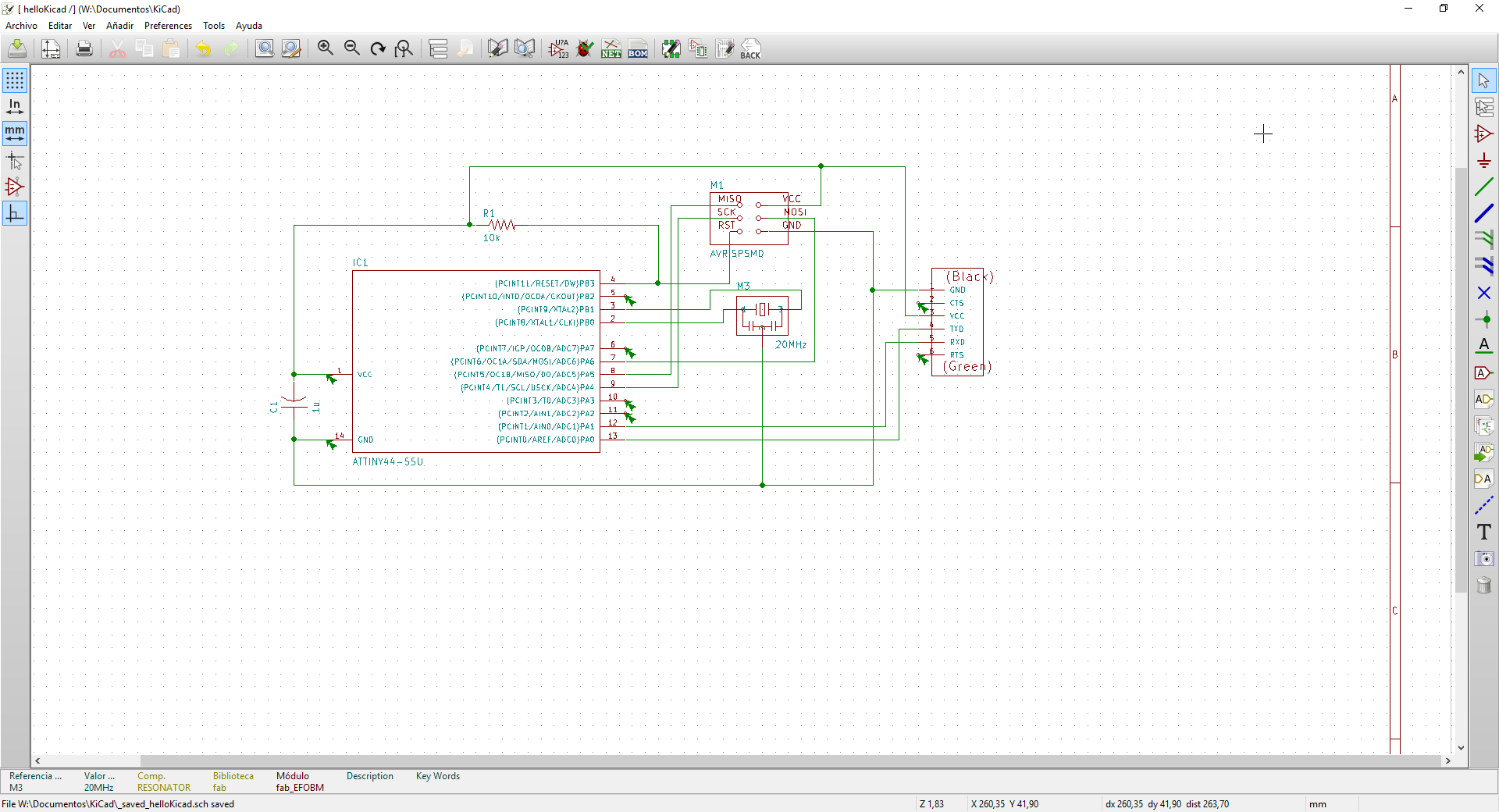
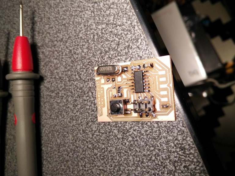
Manufacturing and programming the board are pending!
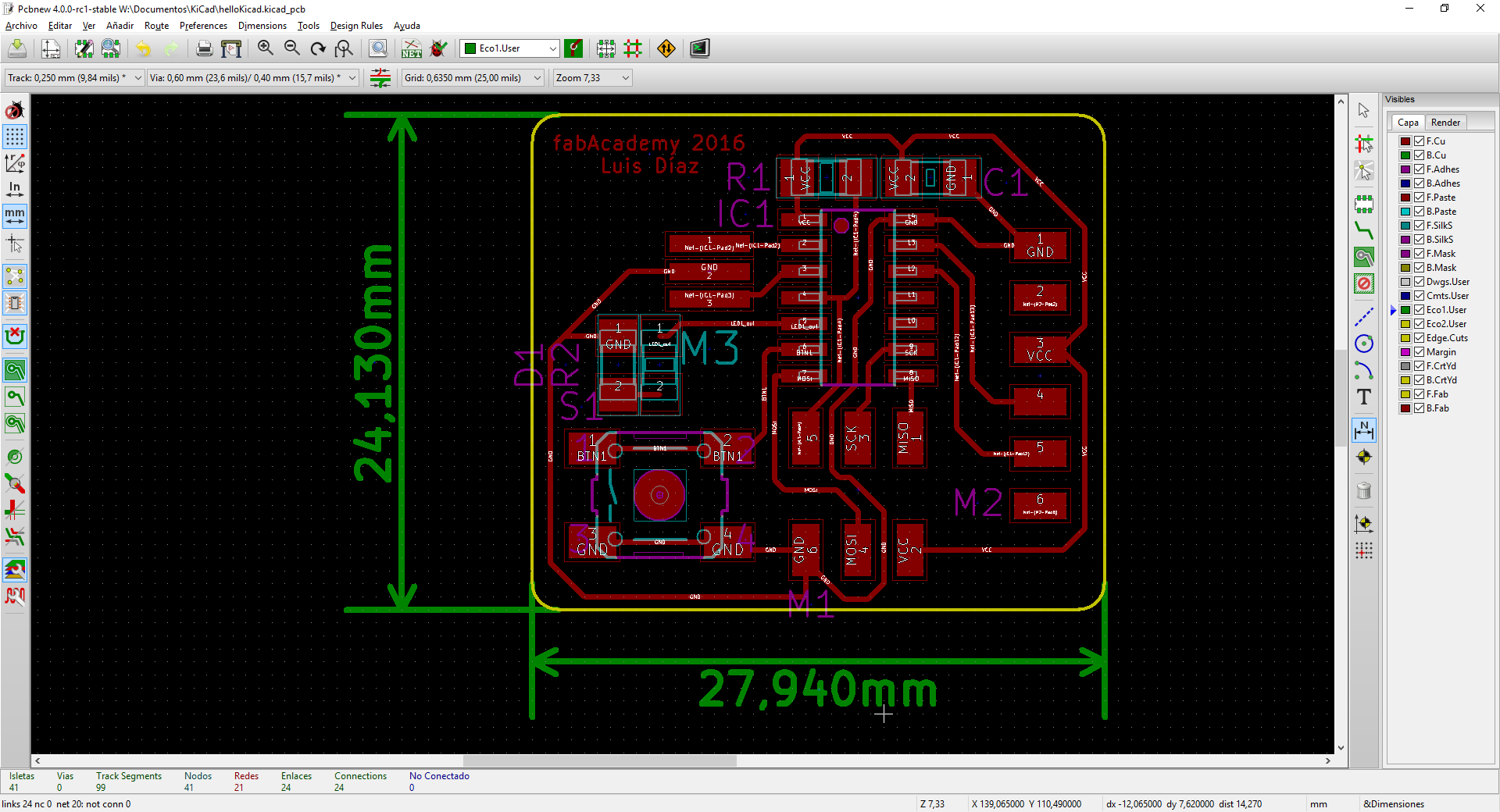
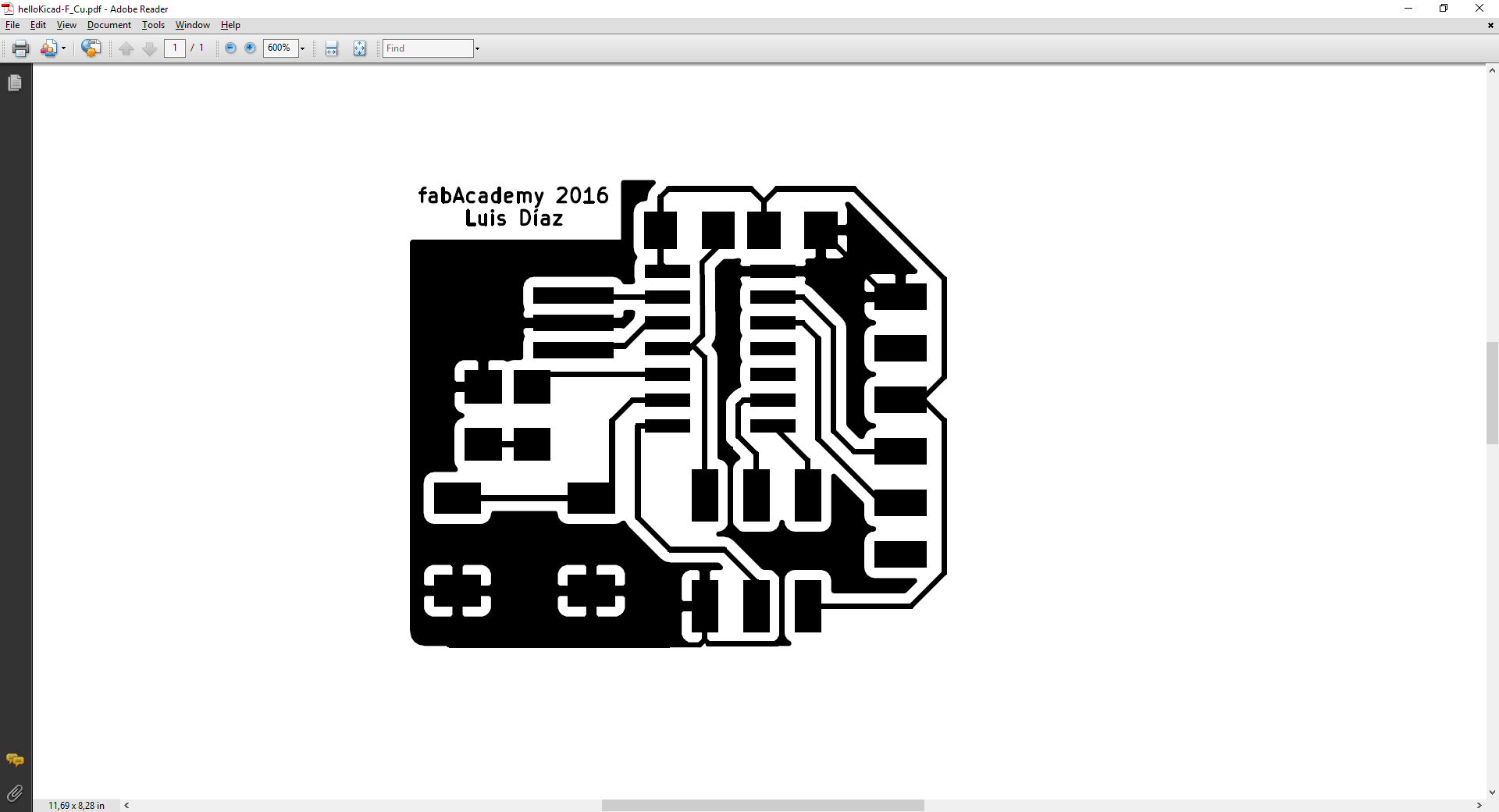
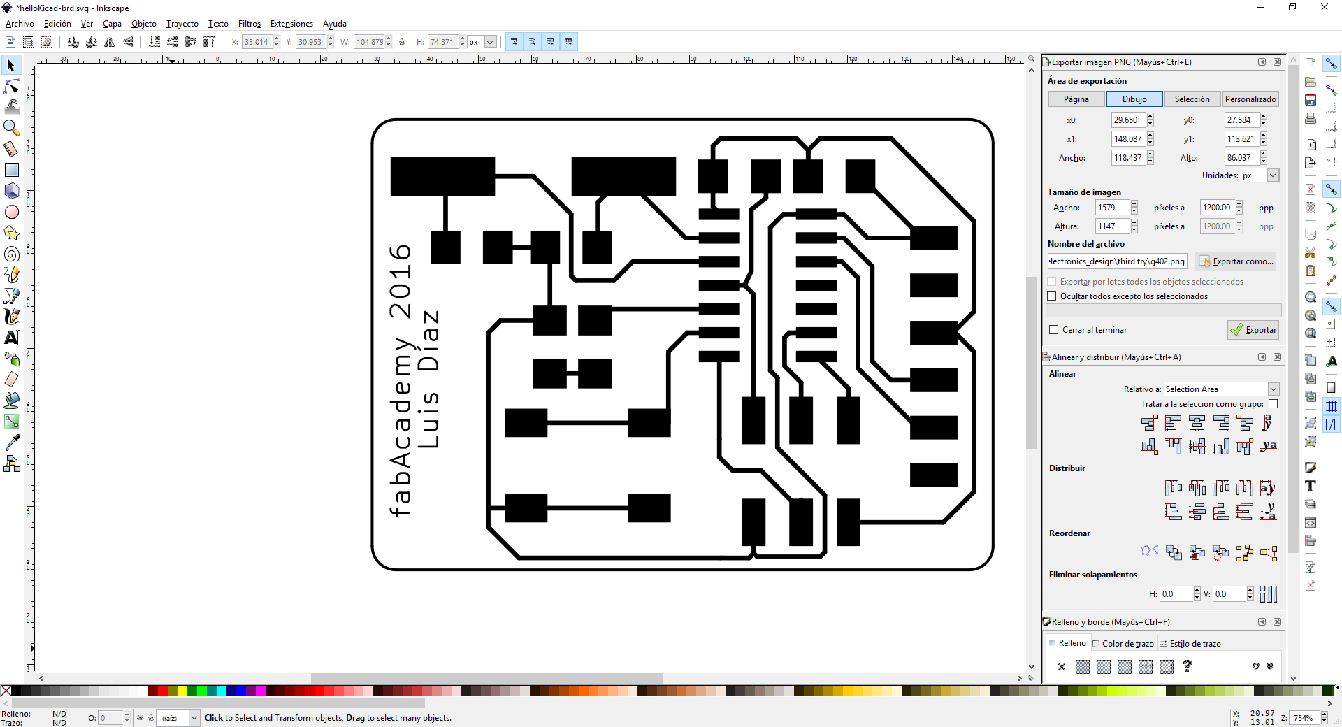
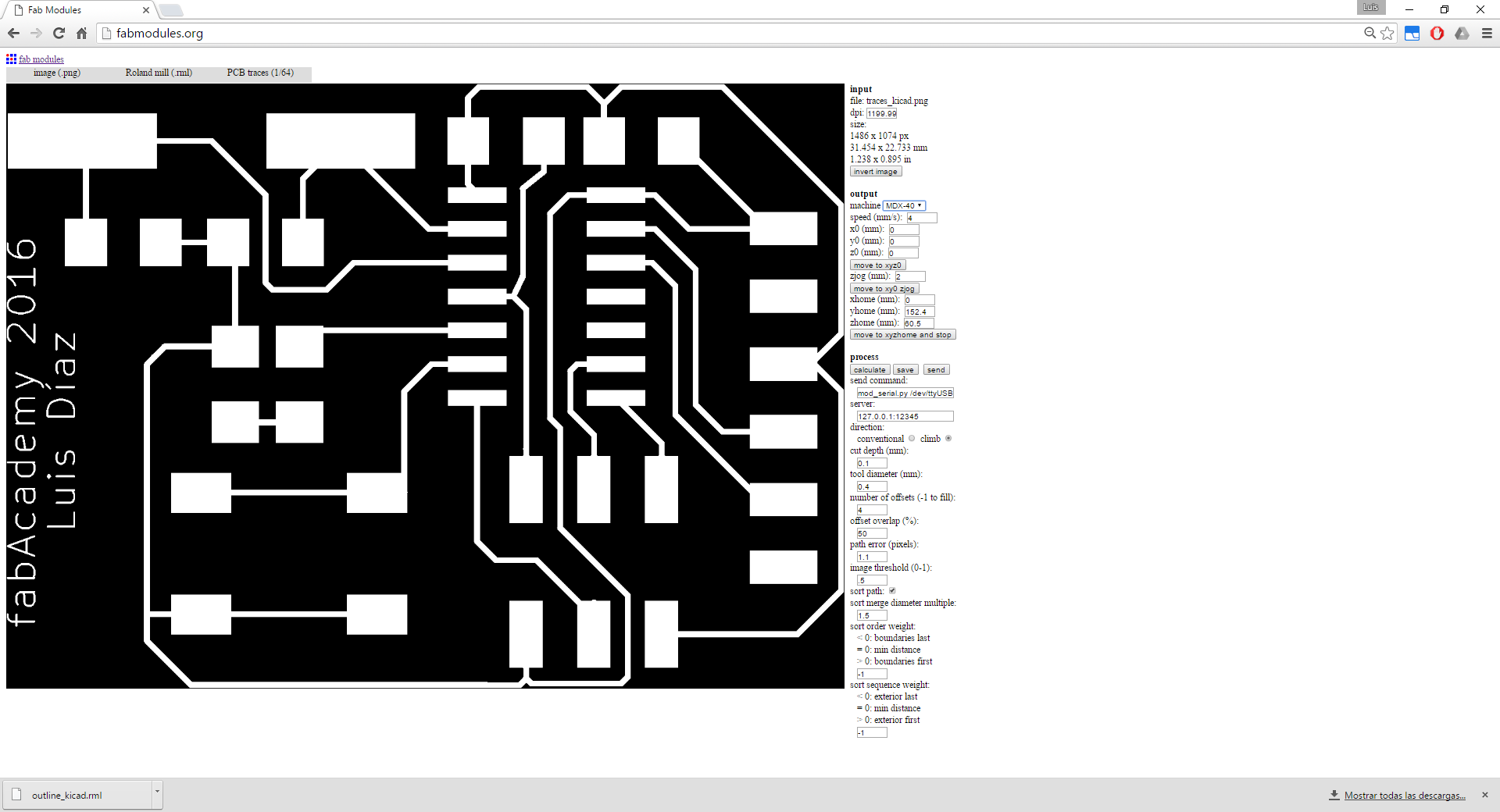
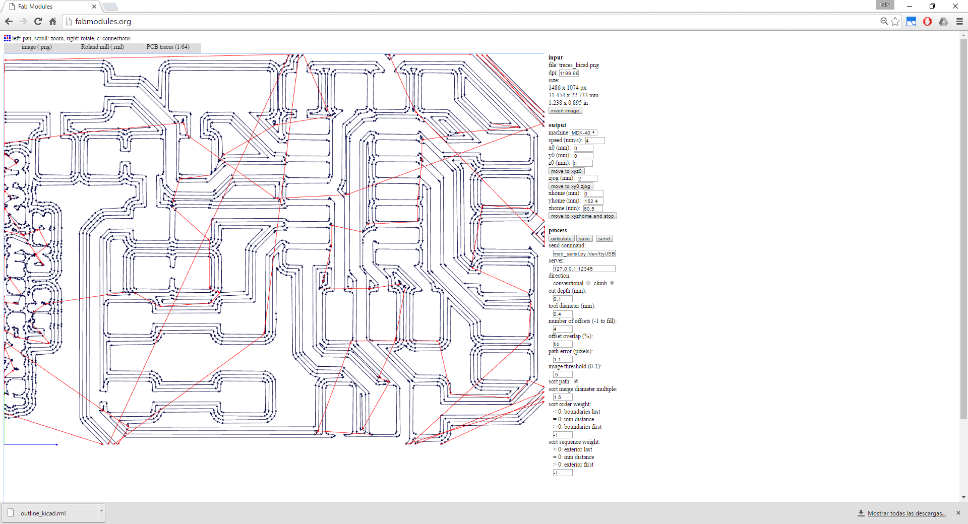
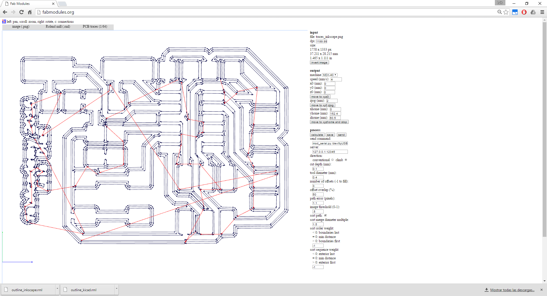
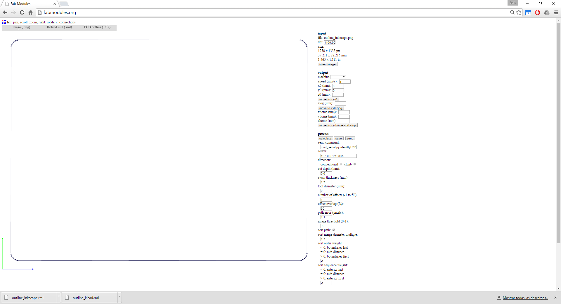
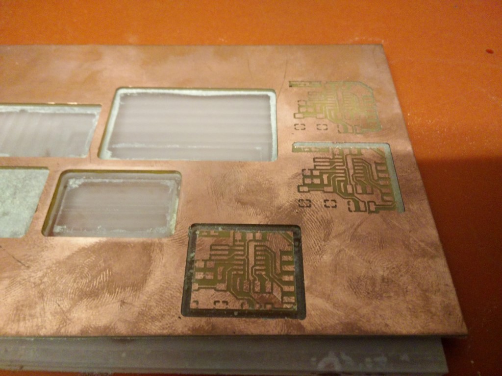
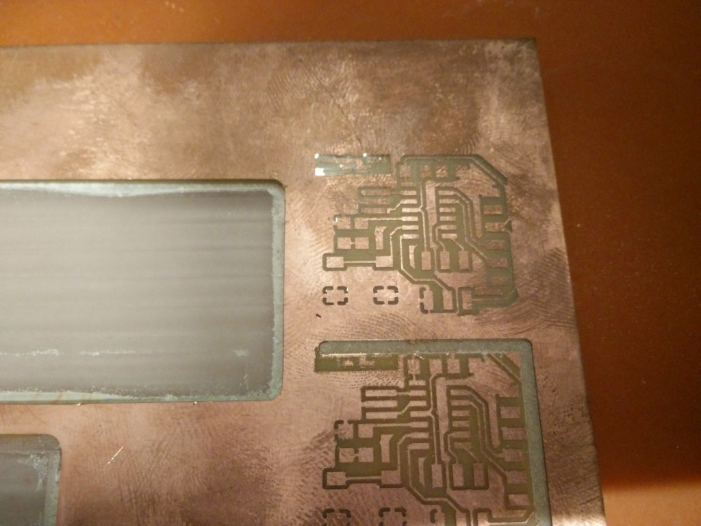
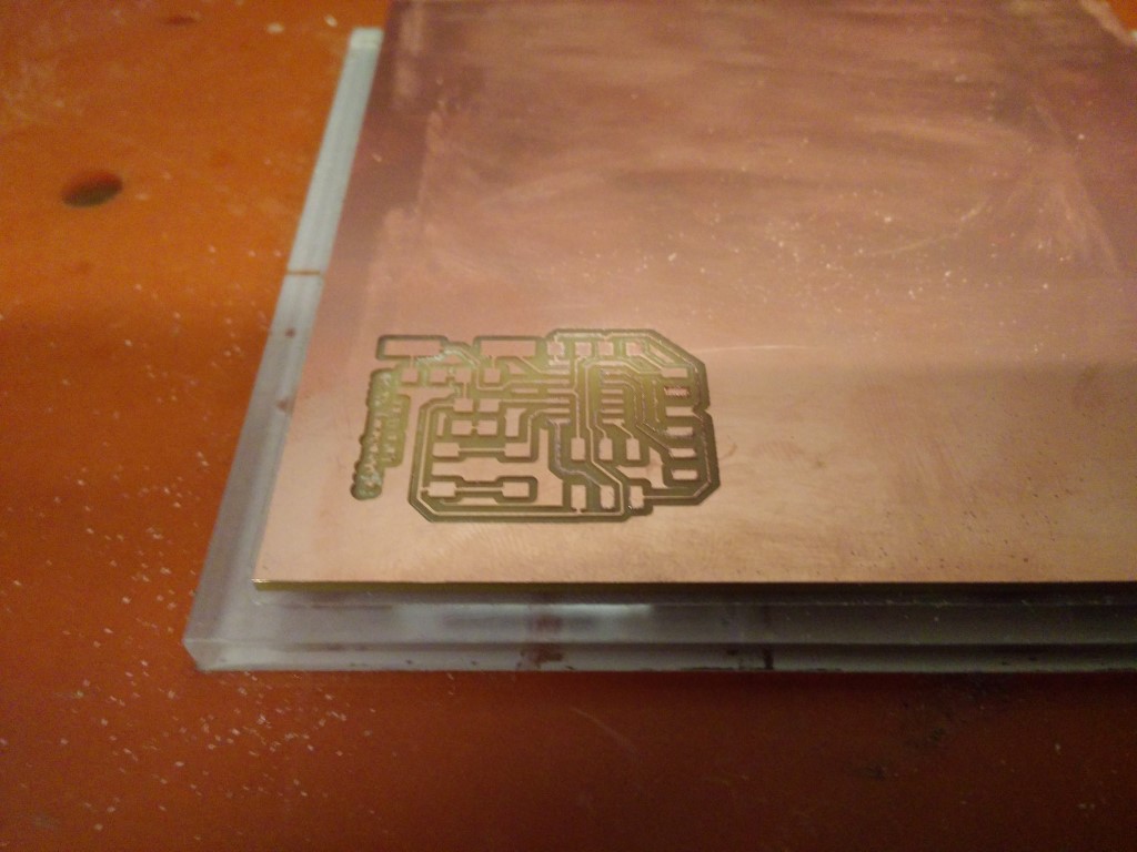
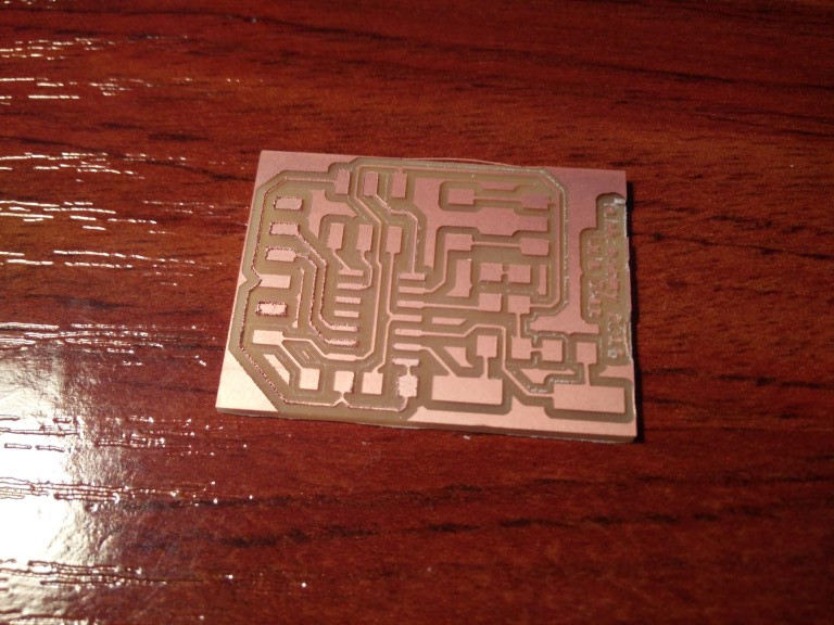
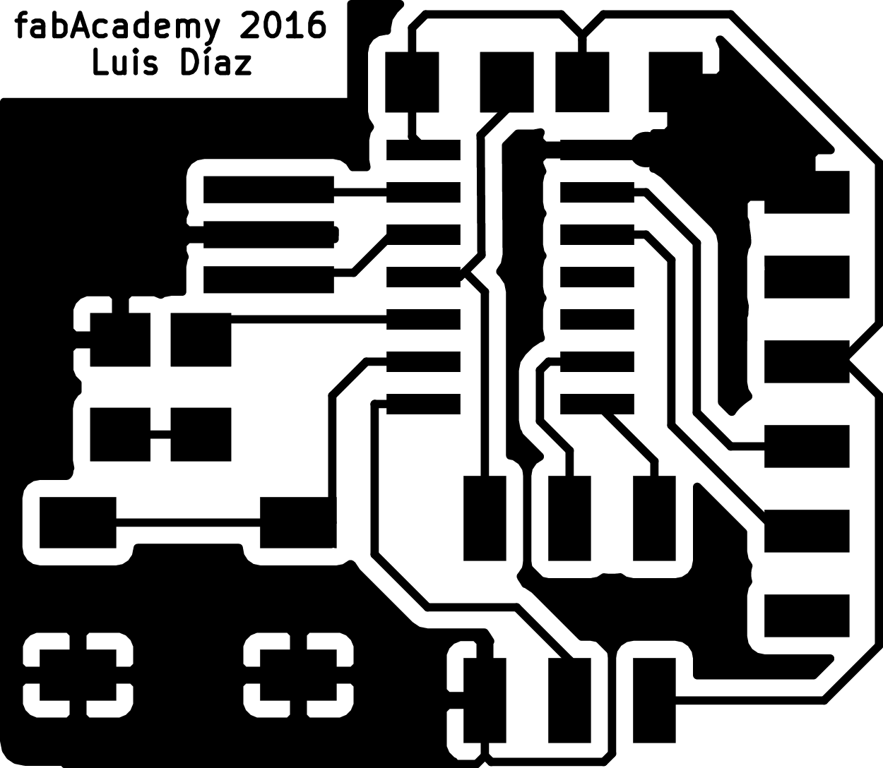
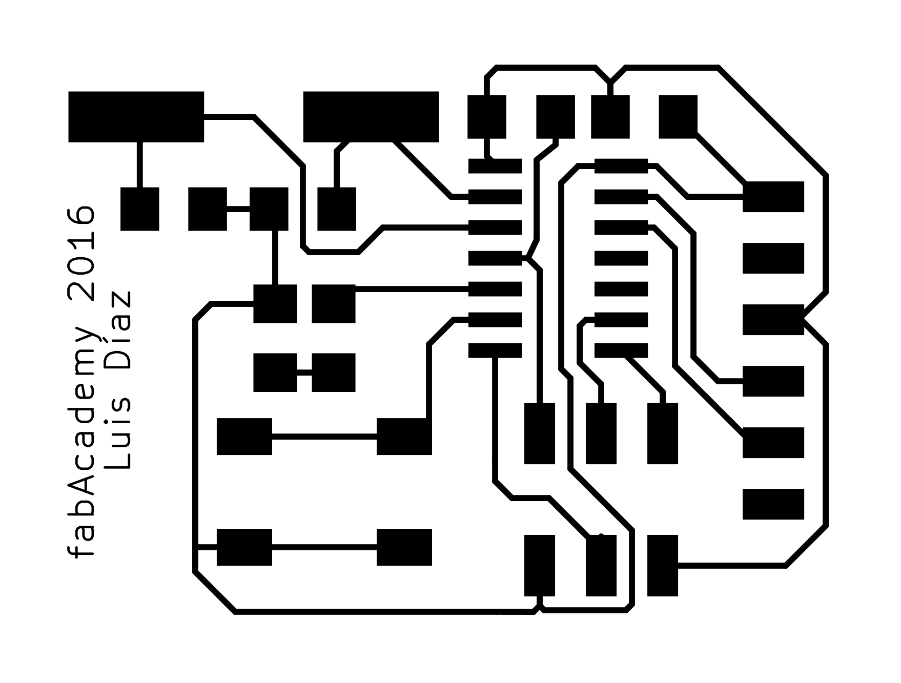
I've planned to do electronics design and input devices both this week, to concentrate board manufacturing now that access to the machines is limited. I've milled the board, but had some issues that needed to be reviewed back home. PCB tracing went good, but when I ran the cutout process, something was wrong and I was destroying the traces, like it was milling the inside instead of the outside of the cut line. This is gonna be my workflow for PCB manufacturing, on week four I've used an existing .png, but now I need to generate my own.
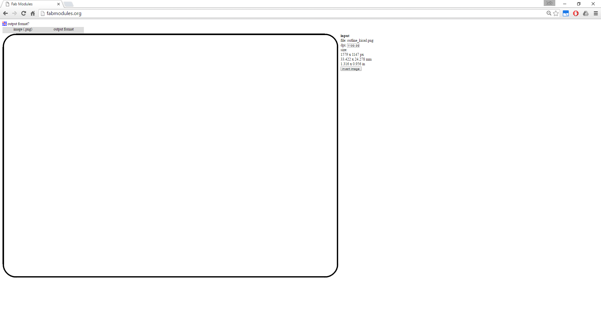
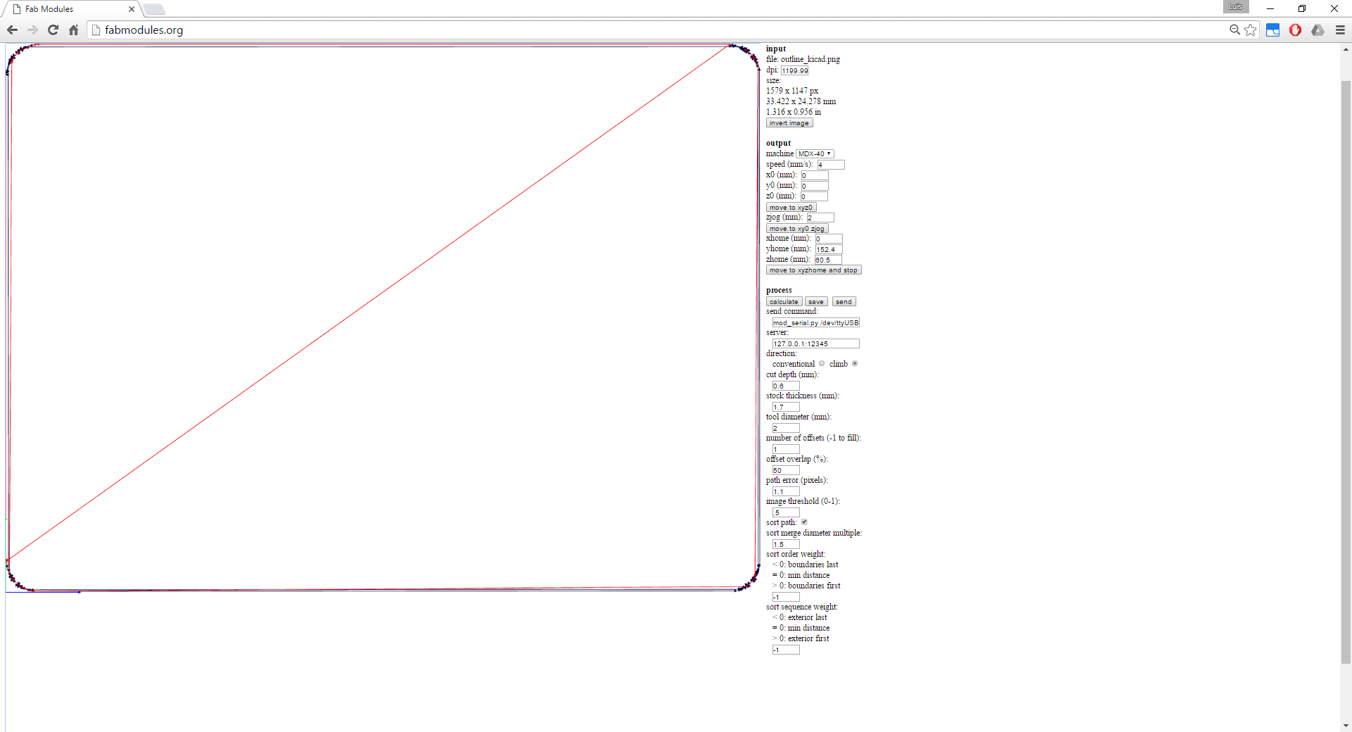
The workflow I've followed was to generate .svg from KiCad and then export as .png each individual process (traces and cut). First problem with traces is that it adjust .png size to vectors, and a border is needed in order for the tool to pass, so a 0.4mm border is needed. Also as I'm using a 2mm mill to cut the board out I'm going to add a 2mm border for cutout .png. Now when I calculate the path with fabmodules.org the path changes as I change the tool diameter. I guess that the rounded corners on the original cutout path made the path try not to get the corner white areas and path was calculated over the black line, instead of going outside the white area on the inside.
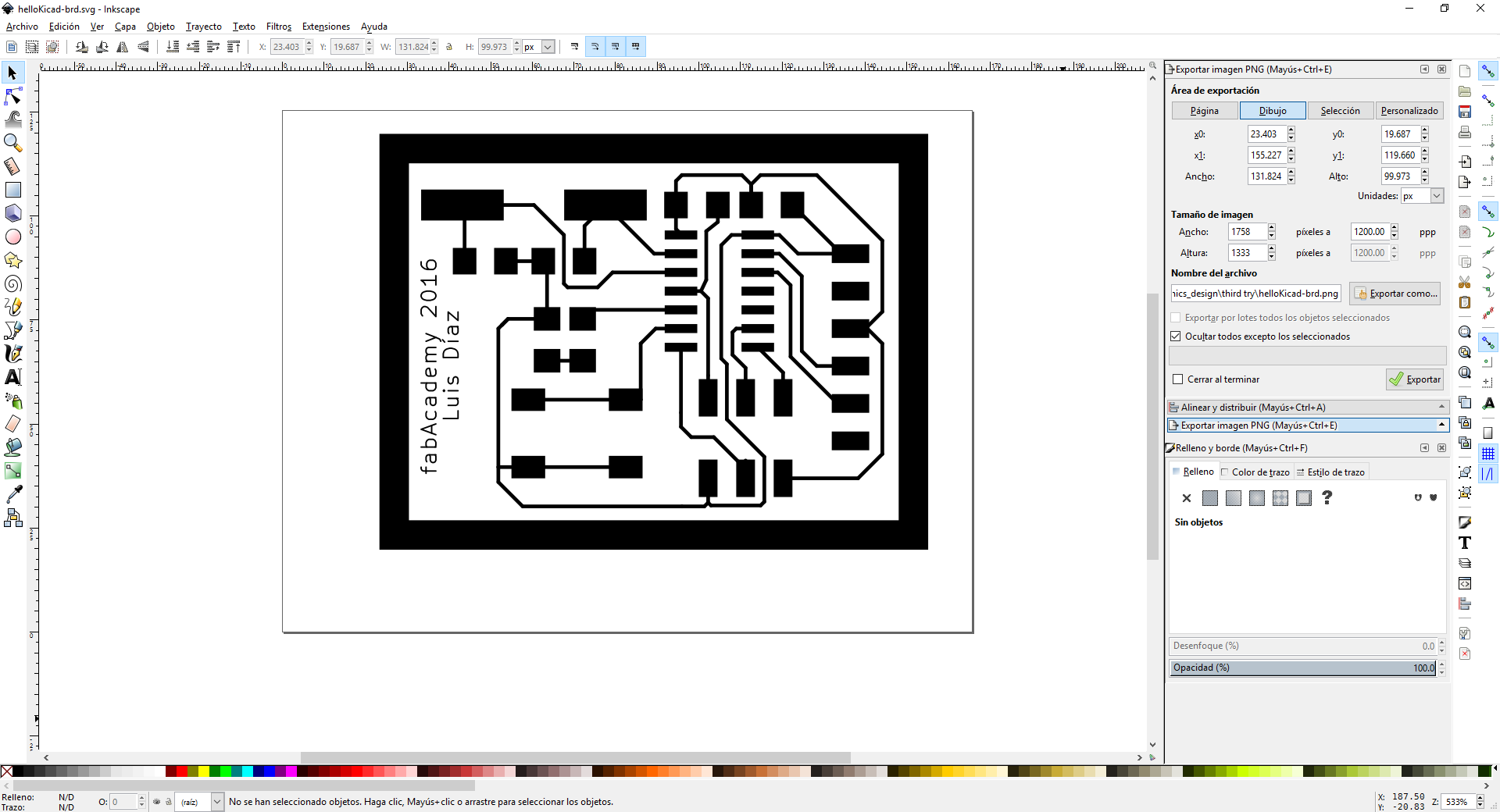
Reviewing the board I've also noticed that the footprint for the oscillator is for one of the fabinventory ceramic oscillators, but I don't have the part so I've had it replaced with an HC49 footprint and had to make the board a bit bigger.
The milling process was a bit frustating due to the problems with the outline that was solved using a proper border size, but learned a lot about the workflow using fabmodules.
Machines and software used
SO: Windows 10KiCad
Roland Modela vPanel
Roland Modela MDX40
0.4mm PCB routing mill (traces) (default fabmodules.org parameters)
2mm PCB routing mill (outline) (default fabmodules.org parameters)
Files
helloKicad.prohelloKicad.sch
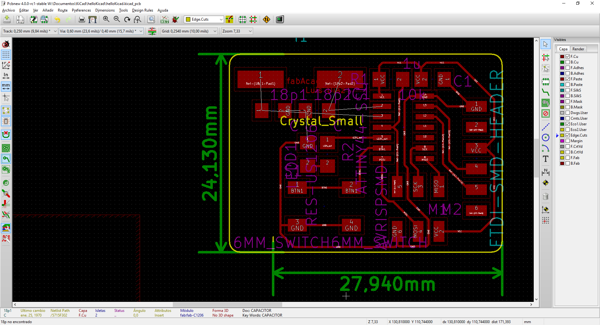
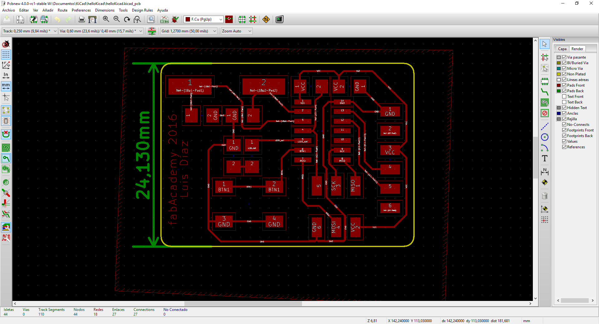
helloKicad.kicad_pcb
helloKicad.net
First version
helloKicad-F_Cu.svg
helloKicad-F_Cu.png
helloKicad-F_Cu.rml
helloKicad-Edge_Cuts.svg
helloKicad-Edge_Cuts.png
helloKicad-Edge_Cuts.rml
Second version
helloKicd-brd.svg
traces
traces rml
outline
outline rml