Week 6: 3D electronics design
March 2 - 9
Assignment
- Redraw the echo hello-world board
- Add (at least) a button and LED (with current-limiting resistor)
- Check the design rules, and make it
EAGLE Design
For this week's assignment, we decided to make a visit to a neighboring FabLab located in Bottrop. It is located and associated with the Hochschule Rhur West. They are a friendly group of fabbers, who we had previously made a visit to. Compared to our lab, they have much more sophisiticated methods of electronic board production, so we thought this was a good opportunity for a field trip. We all packed into a van and headed out into a foggy German morning.
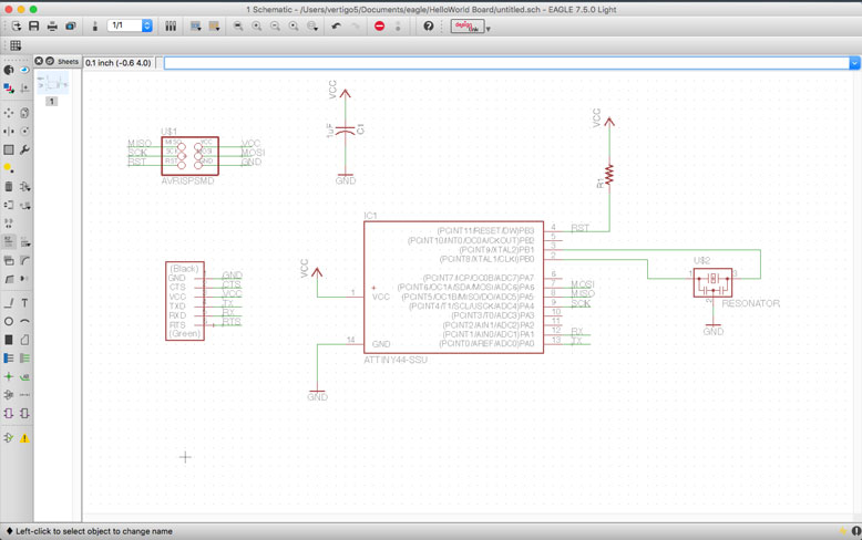
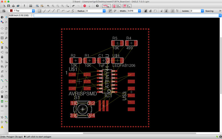
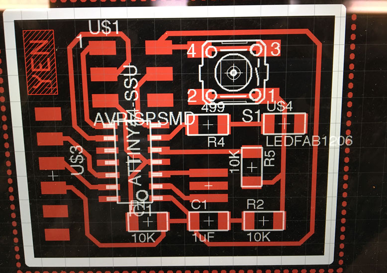
Work began with dropping the required components onto a schematic. Having used EAGLE before for electronics board production, this was the natural tool to use again for this task. Components were are selected and dropped onto the working area. This was relatively easy as all components were available with the Fab comopnent package installed into EAGLE.
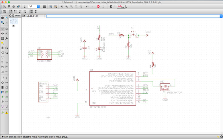
Next came the wiring of the components. It was important to work neatly and orderly, as the more connections were made, the more complex it became. But overall the task went by without much problems.
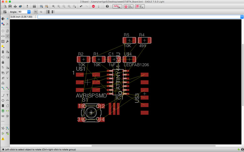
Once completed on the schematic side, I switched over to the board environment to place the components in their final locations as well as plan the traces. The begin, I oriented the chip and the components in a manner where there was mininal overlap.
To help with the process, it was suggested that I create a GND plane encompassing the entire board in order to reduce the number of connections needed to be made. To start this, I created a polygon on the bottom layer.
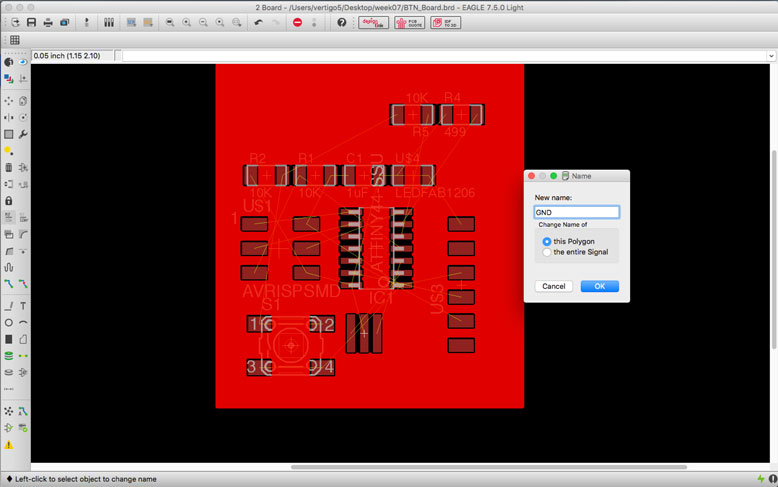
Once the polygon was made, I renamed its name to GND, using the name tool.
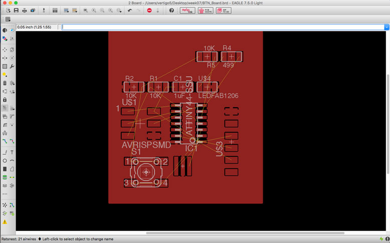
When the polygon was renamed to GND, it formed the connections for all the GND parts of components. Now I only needed to create the traces for the other parts of the components while keeping in mind not to surround any individual GND connections.
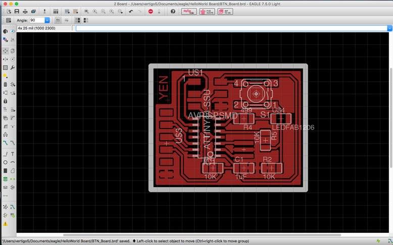
After some trial and error, this is the final design. At some moments it felt like this was an impossible task as one fix for one trace would create problems for others. However, once a few components were moved, all the pieces came together.
Board Production
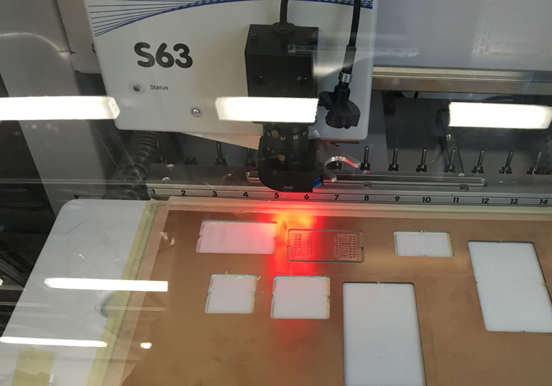
The reason we came to Bottrop was due to their LPKF ProtoMat S63, an automated circuit milling machine. It does auto z-homing, tool changes, and extraction. With a few mouse clicks of my finished board design, the machine started.
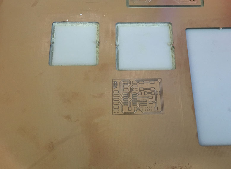
Before I knew it, it was complete and ready for component placement.
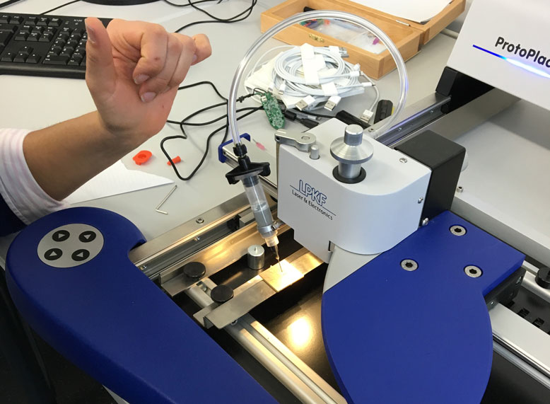
After a few minutes of making sure the traces were clean from any left over copper hairs and particles, we used their manual pick and place machine to drop the components. With a dab of solder paste on the pads, each component was picked up using a suction device and dropped on to the board. We did this with the more harder to place components such as the chip, resistors, capacitors, and crystal.
A double check of the components required, the rest was placed on.
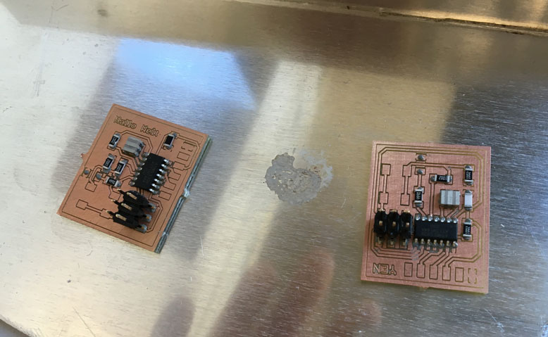
Here are two boards ready to go to the reflow oven.
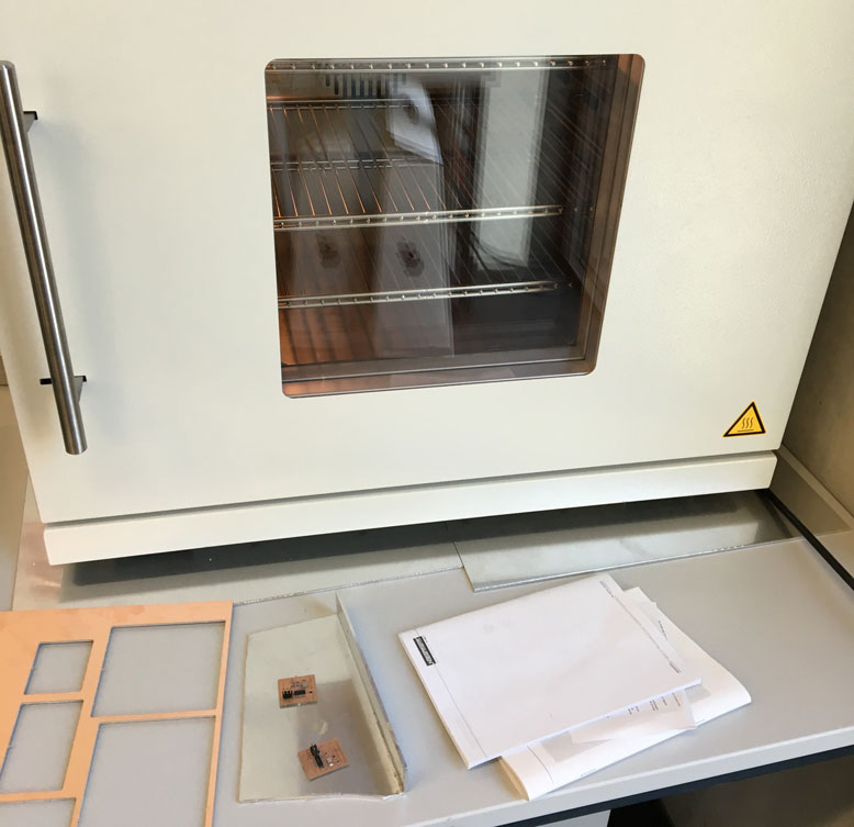
After a few minutes in the oven, the board was ready to go home!