WEEK|04
Electronic Production
For this week's assignments, we had make a PCB of a FabISP. I choose to make a redesign using schematics found here.
Which tools ?
I really don't like Eagle software, even if its a great tool, their stupid board size limitation makes me upset. For some time now, I used to use KiCAD less ergonomic than Eagle but it's a Free Software, and for me, this is important. Since the
CERN is involved in the project KiCAD has made hudge progress, and since version 4.0+, he's way more convenient than before, even if there's still a lot of weirdness in his workflow.
There are other electronic CAD software out there, but for the hobbyists, KiCAD is IMHO a good choice.
Files
Schematics, PCB traces, PCB outline


Did I do that elsewhere ?
Here is the assignements where I had to use these skills :
My workflow
TLDR;
As always when I use KiCAD, I first create a new project. I have all my KiCAD projects on a Dropbox or equivalent, so I can switch my workstation without hassle.
Typical production workflow is something like :
- Create the schematics
- Assign numbers to all the parts (they aren't numbered on creation unless you do this by hand) using the part numbering wizzard.
- Assign a footprint to all the parts, this is one of the differences between KiCAD and Eagle, as Eagle already know witch part has witch footprint.
- Export Netlist
- Launch "pcbnew" for board creation
- Importing Netlist into pcbnew
- Place the components, route the tracks/via, etc...
- Plot, either gerber or SVG or other format
And if later I change my mind, I just need to edit the association, not the whole schematic.
More in details
Schematic
 For this specific exercise, I first made the schematics using eschema, strictly copying the David A. Mellis one.
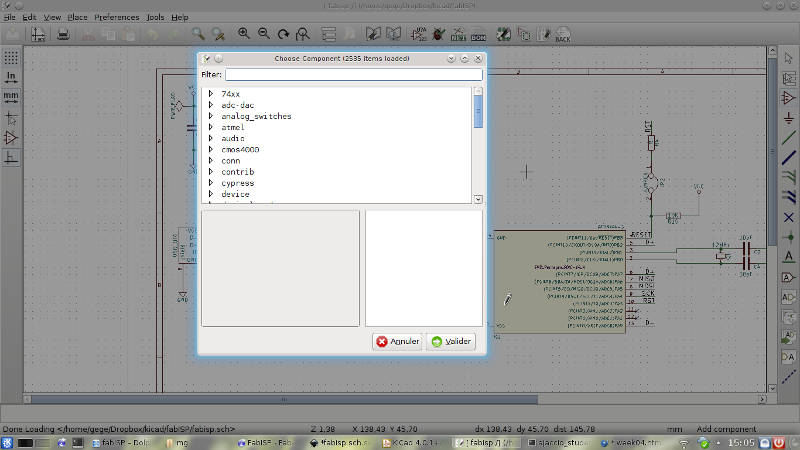
Typing "A" key, KiCAD switch to "add component" mode, displaying a dialog when we can choose the component we need. He stores the last used components to make it more convenient. Anyway, when adding a lot of the same type of components, Instead of always use this dialog, I prefer to "copy" an already placed component using the "C" key while hovering it, great speed improvement !
One all the component placed, I begin the wiring using the "W" key.
If a component doesn't have all its pin connected, KiCAD need to know it, we do this by placing a "not connected" mark (the blue cross) on the pin.
When the schematic is done, we need to annotate the components (setting their reference), either by using the annotation wizard or by annotating manually all the components (witch could be a very boring task).
Associating footprint
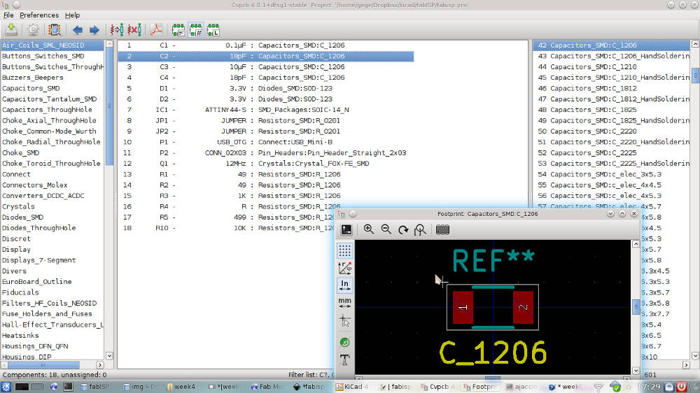 KiCAD needs to know the form factor for all components in a schematic, for this purpose, the "cvpcb" module is used to associate a footprint to each component. This is a boring task but could be very powerful
Anyway, even if the wizard has been greatly optimized over the different release, he still has some weirdness we need to accommodate to.
For each component, cvpcb shows a list of all modules that could be acceptable (we can filter this list either by keyword, pin count or library).
Once this step is done, we need to save the changes, and then go back to eschema to export the netlist.
PCB creation
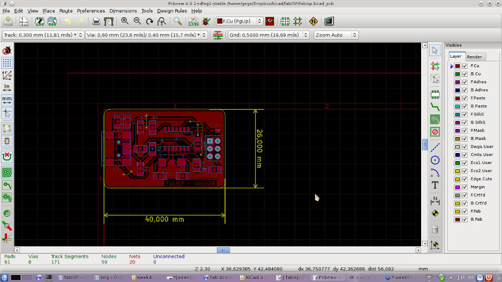
Fire up the pcbnew module and import the netlist, if all went OK, components should now be all superposed on the workspace. We need to arrange them as we wish.
Once all components are place, we need to define the outline of the board using the "Graphic line or polygon" tool. Be careful to select the appropriate layer (Egde.Cuts) or KiCAD will complain about that.
Then, we begin switch to routing mode by typing "X" key.
KiCAD since version 4 have two more graphic rendering engine, when using OpenGL (F11), we can use the new Push & Shove and the "semi-auto routing" function, witch are great ways to gain a lot of time.
Push & Shove will move existing traces to open the way for the path being traced, and the semi-auto routing will suggest different path live.
When the board is finished, we can use the DRC to check if the design rules are respected (they can be set in the "Design rules" menu).
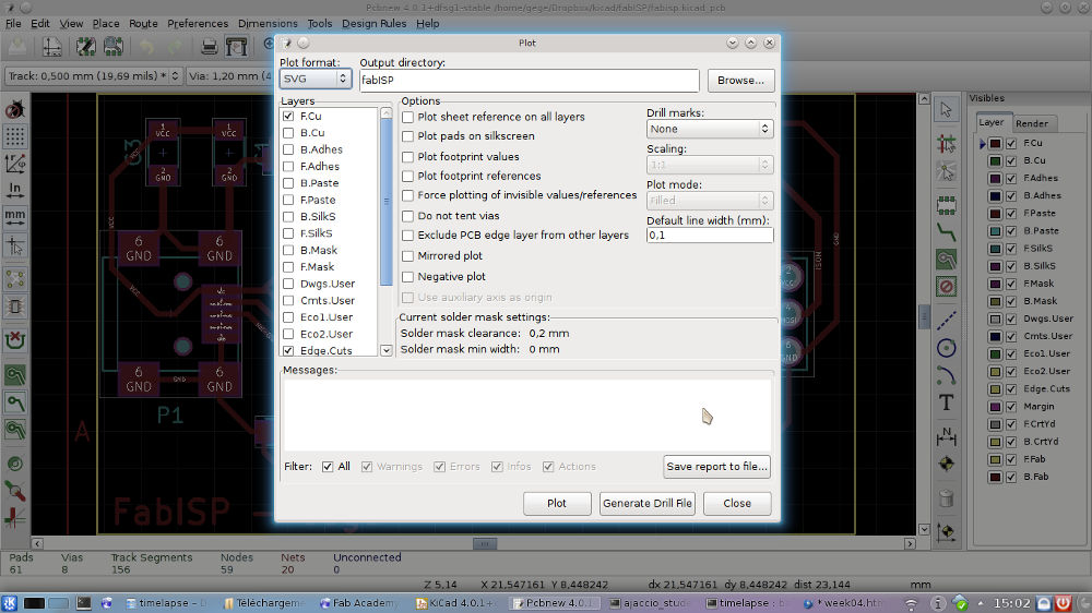
To export the board, we click on the "Plot" button and we select the format and the layers we want to export. In this case, I choosed to export in SVG and only the front copper and the edge cuts.
Pure board conception is now over, next step will be to generate the milling file.
File Conversion
As KiCAD didn't export in PNG directly, and the SVG exported by KiCAD isn't exploitable as this in fabModules, we need to convert it to PNG at first.
For this, I used inkscape, just opening the SVG and exporting it in PNG, just take care you are choosing the drawing as export aera, and don't hesitate to augment the DPI (I used 500).
PCB Fabrication
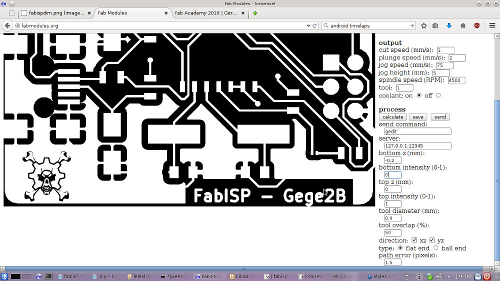
Then, the image file can be loaded up on fabmodules.org
After a few trys, I realized that I needed to choose what process we wish to do before choosing the machine, so the fabmodules auto-completes the settings.
For the first try, I leaved the default and saved the .RML file. That was an error (more on that later).
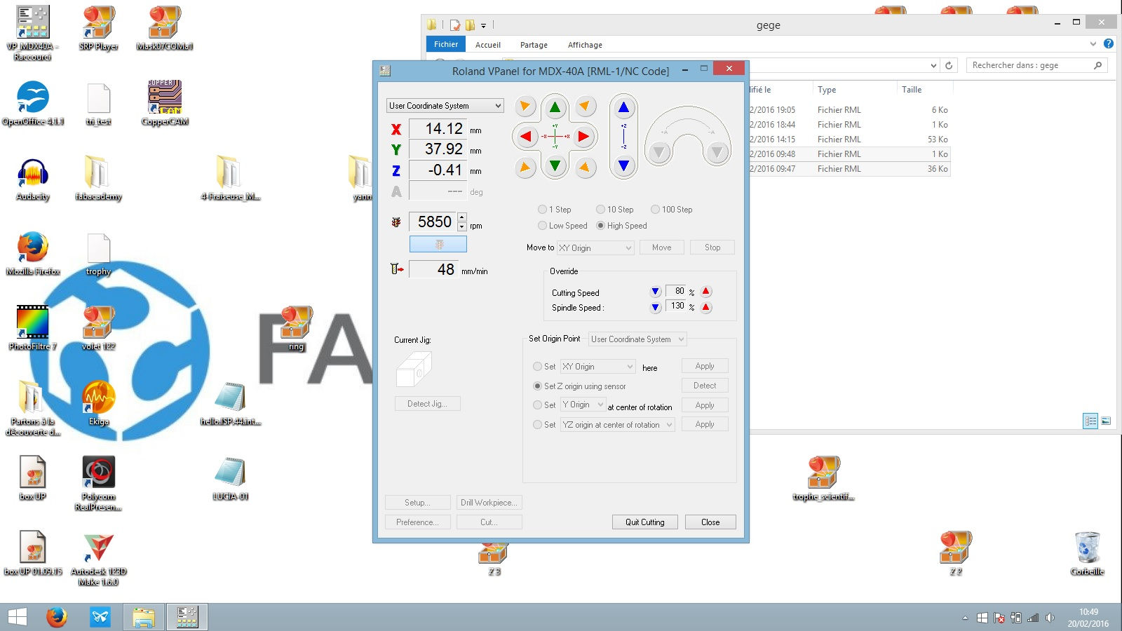
First, as always, I do what is needed on the machine itself (in this case : fixing the copper plate, changing the endmill and do a little cleanup). This way, I can focus on the software setup
So, using the vPanel software for MDX-40, I did set the XYZ origins, I loaded up my .RML file and begin to mill
After some trials and errors and two broked endmill, I got a good board ready to be soldered (more on that few trials later, too).
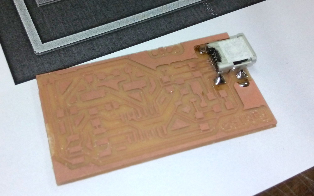
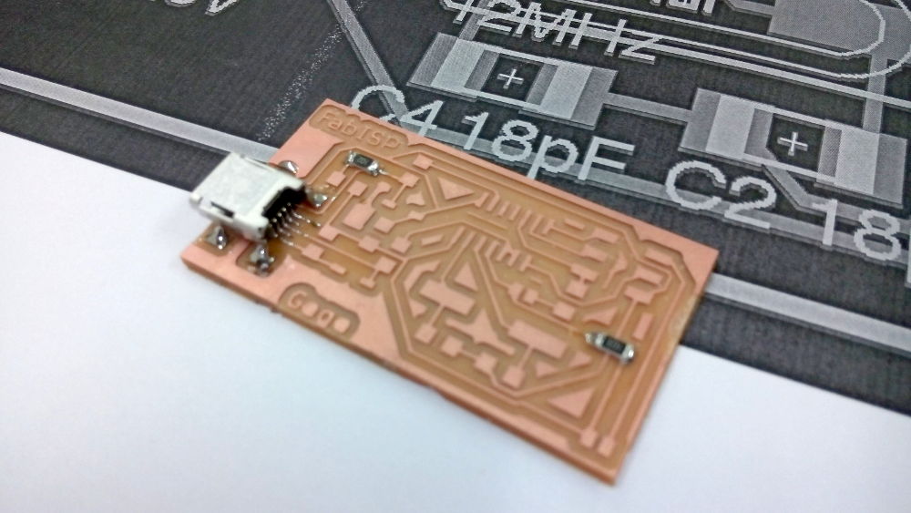
I forgot to take a picture of the freshly milled board, instead, here is the board with the USB connector in place.
As you may see, this isn't the board I designed with KiCAD. This board was a "Plan B" made from David's one and modified with The GIMP to add my name. More on that later, too.
Soldering the parts
I'd already soldered some SMD components, so this wasn't a new thing for me. Using flux pen and tweezers, I placed and soldered components one after another, begining by the USB connector (see above).
On one of the picture, we can see a big ugly blob of solder... More on that later, again.
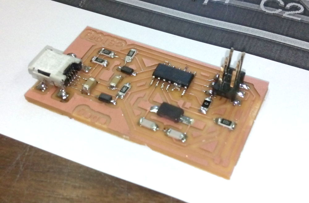
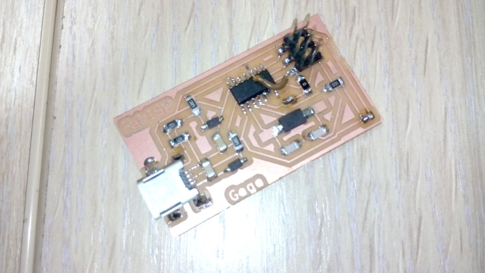 This is the final board. You can see a brown wire connecting ATTiny's pin 10 and RST on pin header (more on that on the "mistakes" part)
Programming the board
After the last checks, I plugged the board and the programmer and run the command to program the fuses and the flash
here are the code :
:~/FabAcademy2016/week4/fabISP_mac.0.8.2_firmware$ sudo make fuse
avrdude -c avrisp2 -P usb -p attiny44  -U hfuse:w:0xDF:m -U lfuse:w:0xFF:m

avrdude: AVR device initialized and ready to accept instructions

Reading | ################################################## | 100% 0.01s

avrdude: Device signature = 0x1e9207
avrdude: reading input file "0xDF"
avrdude: writing hfuse (1 bytes):

Writing | ################################################## | 100% 0.00s

avrdude: 1 bytes of hfuse written
avrdude: verifying hfuse memory against 0xDF:
avrdude: load data hfuse data from input file 0xDF:
avrdude: input file 0xDF contains 1 bytes
avrdude: reading on-chip hfuse data:

Reading | ################################################## | 100% 0.00s

avrdude: verifying ...
avrdude: 1 bytes of hfuse verified
avrdude: reading input file "0xFF"
avrdude: writing lfuse (1 bytes):

Writing | ################################################## | 100% 0.01s

avrdude: 1 bytes of lfuse written
avrdude: verifying lfuse memory against 0xFF:
avrdude: load data lfuse data from input file 0xFF:
avrdude: input file 0xFF contains 1 bytes
avrdude: reading on-chip lfuse data:

Reading | ################################################## | 100% 0.00s

avrdude: verifying ...
avrdude: 1 bytes of lfuse verified

avrdude: safemode: Fuses OK (E:FF, H:DF, L:FF)

avrdude done.  Thank you.

:~/FabAcademy2016/week4/fabISP_mac.0.8.2_firmware$ sudo make program
avrdude -c avrisp2 -P usb -p attiny44  -U flash:w:main.hex:i

avrdude: AVR device initialized and ready to accept instructions

Reading | ################################################## | 100% 0.01s

avrdude: Device signature = 0x1e9207
avrdude: NOTE: "flash" memory has been specified, an erase cycle will be performed
         To disable this feature, specify the -D option.
avrdude: erasing chip
avrdude: reading input file "main.hex"
avrdude: writing flash (2016 bytes):

Writing | ################################################## | 100% 0.74s

avrdude: 2016 bytes of flash written
avrdude: verifying flash memory against main.hex:
avrdude: load data flash data from input file main.hex:
avrdude: input file main.hex contains 2016 bytes
avrdude: reading on-chip flash data:

Reading | ################################################## | 100% 0.71s

avrdude: verifying ...
avrdude: 2016 bytes of flash verified

avrdude: safemode: Fuses OK (E:FF, H:DF, L:FF)

avrdude done.  Thank you.

avrdude -c avrisp2 -P usb -p attiny44  -U hfuse:w:0xDF:m -U lfuse:w:0xFF:m

avrdude: AVR device initialized and ready to accept instructions

Reading | ################################################## | 100% 0.01s

avrdude: Device signature = 0x1e9207
avrdude: reading input file "0xDF"
avrdude: writing hfuse (1 bytes):

Writing | ################################################## | 100% 0.00s

avrdude: 1 bytes of hfuse written
avrdude: verifying hfuse memory against 0xDF:
avrdude: load data hfuse data from input file 0xDF:
avrdude: input file 0xDF contains 1 bytes
avrdude: reading on-chip hfuse data:

Reading | ################################################## | 100% 0.00s

avrdude: verifying ...
avrdude: 1 bytes of hfuse verified
avrdude: reading input file "0xFF"
avrdude: writing lfuse (1 bytes):

Writing | ################################################## | 100% 0.00s

avrdude: 1 bytes of lfuse written
avrdude: verifying lfuse memory against 0xFF:
avrdude: load data lfuse data from input file 0xFF:
avrdude: input file 0xFF contains 1 bytes
avrdude: reading on-chip lfuse data:

Reading | ################################################## | 100% 0.00s

avrdude: verifying ...
avrdude: 1 bytes of lfuse verified

avrdude: safemode: Fuses OK (E:FF, H:DF, L:FF)

avrdude done.  Thank you.
This was the programming of my FabISP, witch we then used successfully to program the FabISP of another student.
Week successful !
"One FabISP to rule them all, One FabISP to find them, One FabISP to bring them all and in the darkness bind them"
In the past
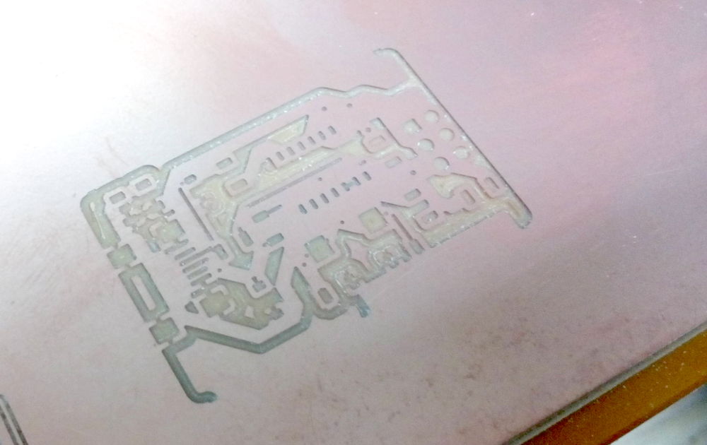
When I was a younger student, at Fred Scamaroni College, I had made some PCB using photosensitive plate and ferric chloride. Unfortunatly, this was a long time ago and I didn't have any pictures of the final boards.
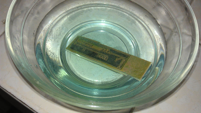 A few months ago, I made some electronic board myself, still using the etching method, but this time I did not use strong chemicals.
I used the toner transfer method, and the etchant was white vinegar and hydrogen peroxyde (H2O2). I documented the method on my blog in french) but here are the different steps :
- Print the PCB on glossy paper using a laser printer
- Clean the PCB with rubbing alcohol or acetone to get rid of any grease on the copper, otherwise this would ruin your efforts
- Place the paper, traces against the copper plate, and heat it with an iron. I used a baking paper to protect the iron. Try to do an even pressure on all the board, for few seconds/minutes
- Soak the board in a bowl of water to rip off the paper, gently scratching the surface, leaving only the black traces
- Put 70% white vinegar and 30% hydrogen peroxyde in a bowl (glass or plastic only)
- Drop the board and wait
- 10. wait
- 20. gently stirr the solution
- 30. GOTO 10
- The solution will become blueish as the copper is dissolved
- maybe you can add some table salt to speed up the process a bit, but be carefull to not over-etch the board
- maybe you will need to add some hydrogen peroxyde or vinegar during the process
- When the unprotected copper is gone, you can rince the board under tap water and TA-DAAAA
I love this method, as we don't need CNC Milling machine and we use only household items
My mistakes
Well, this weeks assignment have been for mow the one in witch I made the more mistakes, ranging from stupid to unpredictable.
First try - Not depht enough
Fabmodules comes with default settings witch are almost good, but on the first try, the cut depht was not big enough so it just scratched the copper.
That wasn't a big deal anyway, With 0.2mm, the cut depht was perfect.
Second try - 1st Broken endmill
The cut depht was good, but then the default milling speed was too high (4mm/s), so I broked an endmill at the middle on the engraving...
Anyway, I still don't know if the endmill broked because of feedrate too high or because this was a used one, may be both ?
Third try - 2nd broken endmill
This mistake was a stupid one : few minutes after having changed the broken endmill, re-doing the Z origin, I launched the job again, end clicked on the "Cutting speed" text zone in vPanel to type 30% instead of 100.
The problem is : this isn't an editable zone. We need to click on the arrows to change the speed... WOops, too late, the head plundged a bit too fast, and BOOM ! An endmill tip stuck in the copper.
Two endmills broked in less than 2 minutes, shame.
Fourth try - Stupidity strokes again
 DON'T FORGET to click "Invert image" button if needed, because the PNG exported with inkscape is a positive (traces are black), so if leaved as this, the traces would be engraved out... Don't make this mistake. I made it. I lost 1 hour. I wasted a board. I lost some hairs.
Ironically, I didn't made this mistake on the first try, because I clicked the "invert image" button, but since the first try, I totally forgotted this step. So this is a really stupid error witch could've been avoided.
Fifth try - Too tiny details
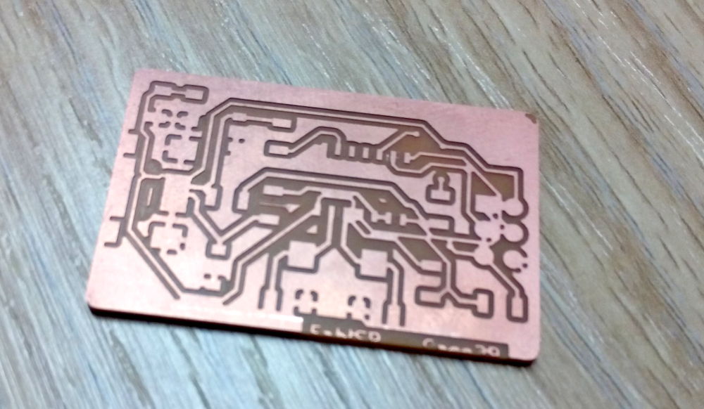
The fifth try was sort of a success, as the milling went without problems, no other endmill were broken, image was inverted before, no fire in the lab etc...
Finally, a board fully engraved, with neat traces.
But on a closer inspection, traces are not so neat. Some are fused together, others are fused with pads, some pads are fused together too... sh*t !
This is when I decided to mill the "Plan B" board - time was running and I feared to not have any board to solder.
While the "Plan B" board was milled, I modified all my KiCAD design, to make traces wider, with bigger clearance between them, etc...
As soon as the "Plan B" board was done, I began soldering it, in the same time, I ran another milling job with my re-designed board.
Soldering
All the soldering went fine, untill the ATTiny44.
I know this component must be soldered in the right orientation, I checked it.
Unfortunatly, I gived a little shake, so the IC went upside-down. I replaced it, but this time without checking his orientation ! I was sure the orientation didn't changed, That was my stupid mistake number 3.
The problem is that when I tried to desolder the IC using braid, I failed and some pads went off .
Fortunatly, two of them wasn't connected, but the other three was. That's the reason of the solder bridge between two pins, they are normally linked together but one of the pad wasn't here anymore
Pin 10 pad is gone too, so I marked it, and later I'll solder a piece of wire from there to the RST on the pin header
Anyway, I checked all pads on the IC to make sure they were all properly connected.