WEEK|11
Input programing
For this week, we had to design a board, integrating a sensor, and read it.
Software used
- KiCAD
- Code::Blocks
- Avrdude
- Fabmodules
- Inkscape
- Git
Source files are available here :
Did I do that elsewhere ?
Here is the assignements where I had to use these skills :
My idea
My idea was to make a light barrier, witch will be used to trigger a bell/song when someone enter in the fablab.
Indeed, right now, there is no such thing, and if the fabmanagers are busy in another room, they just can't know that someone is here.
To add a little more usefullness to this project, I added some constrains :
- Trigger the bell only when someone enters, not when they are leaving. So I need to detect the direction
- Use only one sensor/interrupt, because ATTiny45 is poor in I/O
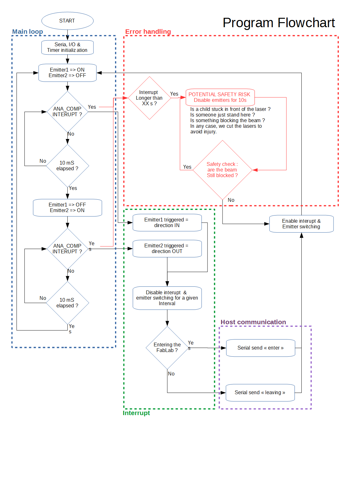
I made a diagram of the program flow (neither perfect nor complete, just a reminder for me), so you can see the logic behind this project.
There is not a strict reading of the sensor, instead, the sensor value is compared to a reference value (tuned by the varistor), and if it is greater, it triggers an interrupt (ANA_COMP vector), witch then sends a command via the serial port.
Board conception
The board will be based on my work done for the Week 6, but will use an ATTiny45 instead of the ATMega, and of course will have a photo-darlington embbeded.
Designing the board was nothing new, but this time, I learned from my previous mistake (that's the goal, isn't it ?)
- I used strict clearance and track width, just enough so I can still route tracks from/to tiny pads.
- I made some component footprint for the SMD pin headers instead of using throuh-hole ones.
- When exporting the board to SVG, I included the outline in the Copper side, so the traces file and the edge cut will be perfectly aligned (but of course, I made another mistake instead...)
Technical choices
For this project, I had two alternatives :
- Using two sensors and two light emitters, and apply some logic-magic to determine the direction,
- Using only one sensors and two light emitters, plus a clever charlieplexing, and apply some logic-magic to determine the direction.
And because it only use one sensor instead of two
And because just reading a sensor would be boring, sorry.

At first, I wanted to use two laser pointers keychain slighlty hacked to allow them to be driven by my board, but I didn't find any in the local stores at proximity. So, for now, I use two LED.
To allow further modification, I used two 1x2 pin header on the board, so I just have to solder LED or Laser(+ transistor) on connectors to switch them as soon as I got my hand on two cheap laser keychain.
About this point, I didn't tinker enough (by lack of time), and I think I will face some troubles when switching for lasers. Charlieplexing works "out of the box" for the two LED right now, but I think I will need additionnal components when putting lasers instead. Here is what I plan to do :
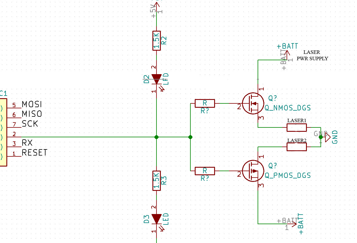
In fact, I still don't kown if I'll switch their power supply on and off, or if I'll shunt their switch button with the mosfet. One thing is sure anyway, I will put a common power supply for both of them to allow an easier battery replacement
Creating custom footprint
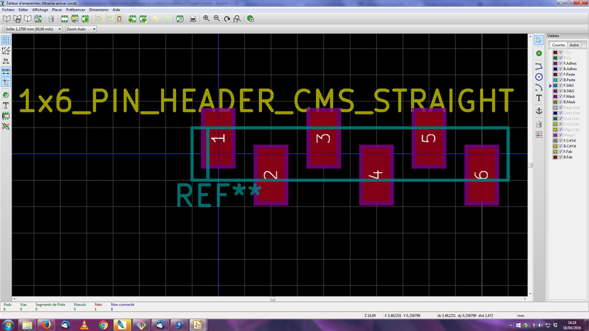
KiCAD comes with a lot of footprint, but seems to miss a lot, too. Notably, I cannot find any SMD pin header footprint, so I decided to make my own, using this document or this one as a references for the dimensions. I made a serie of 1-row pin header (up to 6 pin) for straight and right-angled headers, and a serie of 2-rows (up to 2x04 pin).
Later, I also made a footprint for the SMD 16MHz resonator (using this document)
The new version of footprint editor is better, we just need to create one pad with all the properties correctly set, and use the "create matrix" command using the right-click. Entering the number of pads we want in both direction, their spacing, some other options could be tuned. When we click on OK, KiCAD's Footprint editor create all the pads according to our requirements.
All the footprint are available in the link on top of this page
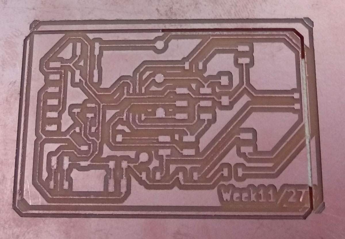
Routing the board
This was done without much efforts, I just been carefull of clearance and track size. When using SMD component and milling machine, this could be a problem because too much clearance would avoid traces to be connected to IC's pads, and not enough will fuse traces together. For this board, I set clearance and track size at 0.4mm and that was just enough.
While I was working with KiCAD, my co-student Yann was on Eagle and lost some hairs :-)
I don't know Eagle very well, and we will all agree that KiCAD isn't an example in terms of ergonomy, but I think, according to what I've seen, that Eagle is even worst !
Exporting SVG and PNG
When plotting the SVG, and unlike the last time, I unchecked the "Exclude outline from all layers" box.
Indeed, for the last milling job, I got some little trouble with outline cut being really close to the traces. After some tinkering, I guess that - as I was exporting the traces without board outline - they was off-center
Milling the PCB
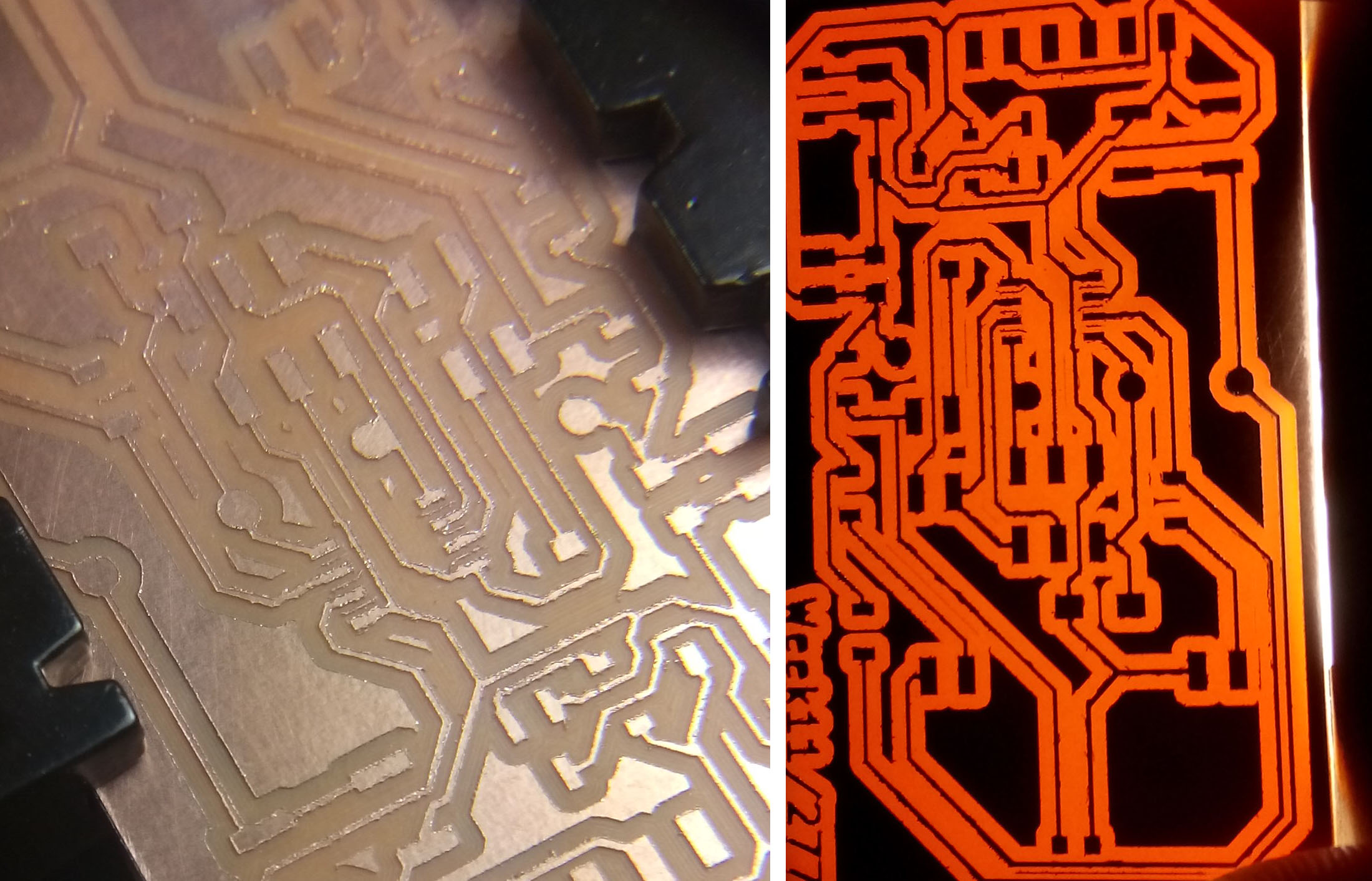
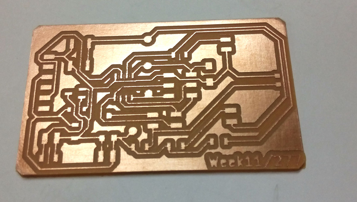
I was right ! This time, the traces and the outline cut was perfectly centered (on the second try... More on that later.)
But, as you can see on the picture, traces are very ugly. The endmill wasn't fresh and this leaves all this little shears on traces. Fortunatly, after a bit of sanding with a fine grain sand paper, things was a bit less messy, but still not perfect.
Anyway, there was neither shorts nor cuts in the traces, good thing.
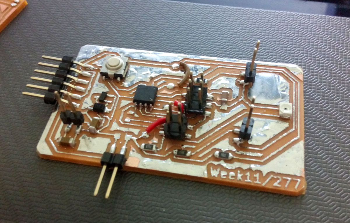
Soldering the PCB
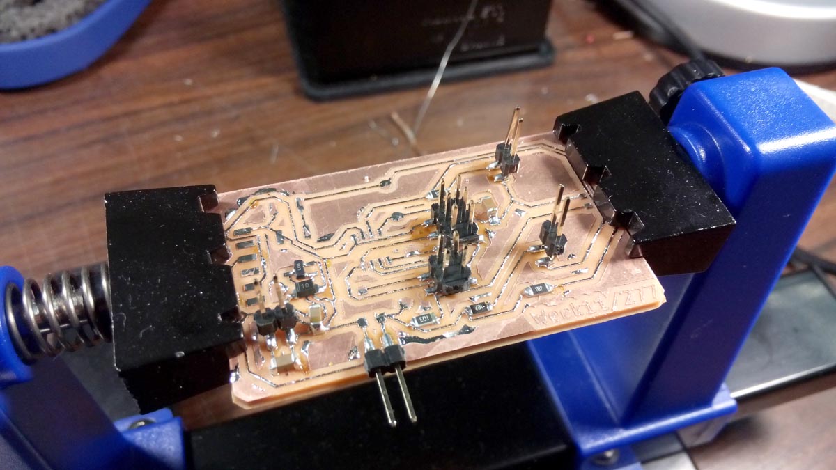
Soldering went without trouble, except for two components.
The ATTiny, for witch I selected the wrong footprint in KiCAD (a narrower one), so I had to fold his pins under the package to be able to solder him. Tricky, but it worked.
I also made a mistake when creating footprints for some pin headers (the single row, straight ones), I aligned the pads instead of offseting them a little bit (0.6mm). So I had to use pliers on right-angled pin header, to fold their pin by keeping them aligned. Waste of time, but it worked too.
All the remaining components was soldered without problem.
Oh, and PCB vice are MUCH usefull than third-hand when it comes to maintain PCBs in place !
Tinning the board
As mentioned above, traces was very thin and crappy on some spots, so I decided to tin all the traces using lot of flux and solder iron. This was really easy. Once the board finished, I decided to tin also the remaining copper islands, even if this wasn't necessary.
Tinning after the component was soldered isn't a great idea anyway :)
Testing the board
Once the board was finished, I hooked up the FTDI cable, the FabISP and Go!
gege@ultron:~/FabAcademy2016/week11/lightbarrier$ sudo make program-usbtiny
avr-objcopy -O ihex lightbarrier.out lightbarrier.c.hex;\
avr-size --mcu=attiny45 --format=avr lightbarrier.out
AVR Memory Usage
----------------
Device: attiny45

Program:     440 bytes (10.7% Full)
(.text + .data + .bootloader)

Data:          1 bytes (0.4% Full)
(.data + .bss + .noinit)


avrdude -p attiny45 -P usb -c usbtiny -U flash:w:lightbarrier.c.hex

avrdude: AVR device initialized and ready to accept instructions

Reading | ################################################## | 100% 0.01s

avrdude: Device signature = 0x1e9206
avrdude: NOTE: "flash" memory has been specified, an erase cycle will be performed
         To disable this feature, specify the -D option.
avrdude: erasing chip
avrdude: reading input file "lightbarrier.c.hex"
avrdude: input file lightbarrier.c.hex auto detected as Intel Hex
avrdude: writing flash (440 bytes):

Writing | ################################################## | 100% 0.45s

avrdude: 440 bytes of flash written
avrdude: verifying flash memory against lightbarrier.c.hex:
avrdude: load data flash data from input file lightbarrier.c.hex:
avrdude: input file lightbarrier.c.hex auto detected as Intel Hex
avrdude: input file lightbarrier.c.hex contains 440 bytes
avrdude: reading on-chip flash data:

Reading | ################################################## | 100% 0.57s

avrdude: verifying ...
avrdude: 440 bytes of flash verified

avrdude: safemode: Fuses OK (E:FF, H:DF, L:62)

avrdude done.  Thank you.
Here we go ! for now, the program uploaded does nothing, I still need to write it, but the board is fully working !
Coding
AVR Code
For the code, I knew I would need to use :
- Analog comparator and his interrupt Page 119
- Interrupts Page 48
- Timers Page 65
- Basic I/O Page 53
Lasers / LED are only connected on one pin of the MMCU, so when idle, the main loop mainly switch this pin HIGH and LOW every 10ms. Doing so, and by using charlieplexing, when a Laser/LED is ON, the other is forcefully OFF.
Inside this loop, the program regularly checks for the states of a boolean variable, witch is set to true on Analog compare interrupt.
As soon as this variable is true, the program enter in a procedure to determine the direction, according to witch state is the laser pin at this moment, sends the corresponding value on the serial pin, and waits for a given interval before returning to the "idle" state.
I used analog compare interrupt, because I didn't wanted to poll the ADC in a loop, this makes the possibility to have the program doing many things instead, and just react on ana_comp interrupt. Well, I agree that, for this particular case, this wasn't really necessary.
Host python code
I really had no credit for this code. By lack of time, I simply copy/paste the example given by Neil, and adapted it a little for my application.
Basically, I simply changed the char byte he was reacting to, and modified some text.
My mistakes
This week was the return of mistakes
Better + Better = Worst.
Cryptic title, huh ?
When in fabmodules for preparing my PCB and outline, I changed the X and Y offset to account for the off-center problem seen on my last PCB.
Of course, at this time, I had forgotten that I checked the "Exclude PCB outline from other layers" box, solving this problem at the source.
So, when came the outline cut, what a surprise !
The cuts was perfectly centered, but as I added a 2mm offset in X and Y direction, well, no comment.
MMCU Mismatch
Fortunatly, nothing bad, phewww...
gege@ultron:~/FabAcademy2016/week11/lightbarrier$ sudo make program-usbtiny
avr-objcopy -O ihex lightbarrier.out lightbarrier.c.hex;\
avr-size --mcu=atmega328p --format=avr lightbarrier.out
AVR Memory Usage
----------------
Device: atmega328p

Program:     440 bytes (1.3% Full)
(.text + .data + .bootloader)

Data:          1 bytes (0.0% Full)
(.data + .bss + .noinit)


avrdude -p atmega328p -P usb -c usbtiny -U flash:w:lightbarrier.c.hex

avrdude: AVR device initialized and ready to accept instructions

Reading | ################################################## | 100% 0.01s

avrdude: Device signature = 0x1e9206
avrdude: Expected signature for ATmega328P is 1E 95 0F
         Double check chip, or use -F to override this check.

avrdude done.  Thank you.

Makefile:30: recipe for target 'program-usbtiny' failed
make: *** [program-usbtiny] Error 1
Woops... Wrong MMCU in Makefile...
Wrong MCU footprint
As you can see in this picture, the Attiny45 had his pin folded, because I choosed the "narrow" footprint instead of the "wide" one in KiCAD Footprint selection tool. Ugly but working hack