Electronics Design
Introduction
Lets discuss what I plan to work on in this week. This week task is Design & Build a Hello World Circuit Board. Therefore, I looked for Hello World Circuit Board in google and I found the Diagram of the Board.
Moreover, to design the board in Eagle software I need to install first the library Fab.lbr.
Schematic Design
I have downloaded eagle cad from Autodesk and reviewed basic tutorials on how to start using the application Eagle Tutorial .
Download the library file Fab.lib. . Copy the downloaded file into lib folder of eagle CAD. And open & use from within the EagleCad.
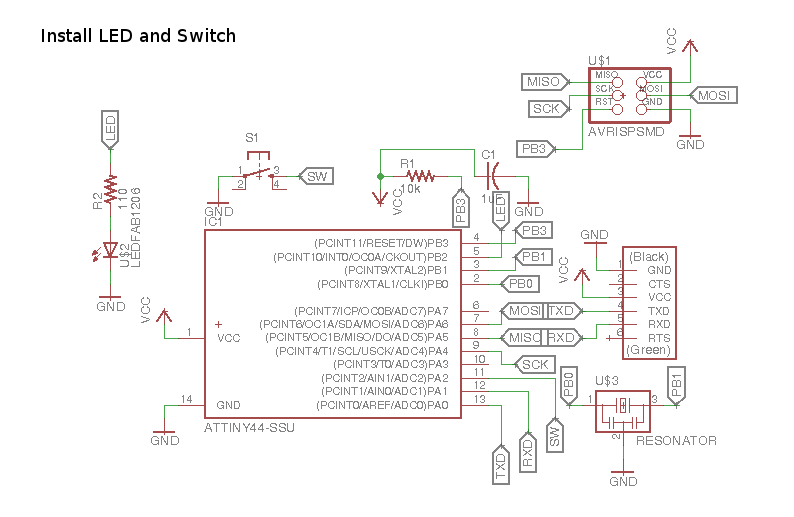
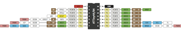
Now for adding the elements we Click Add Icon → it takes us to the elements library. Scroll down to fap and underneath it we find all the require elements for this lap assignment. Double click on the element → it will be added on the worksheet. Click escape → take us back to the select element → another element and so on. Below are the elements to be selected:
1) Attiny44
2) 20mhz resonator
3) 10k resistor
4) 110 ohms
5) 1uF capacitor
6) 6 mm switch
7) LED
8) FTDI SMD Header
9) AVRISPSMD
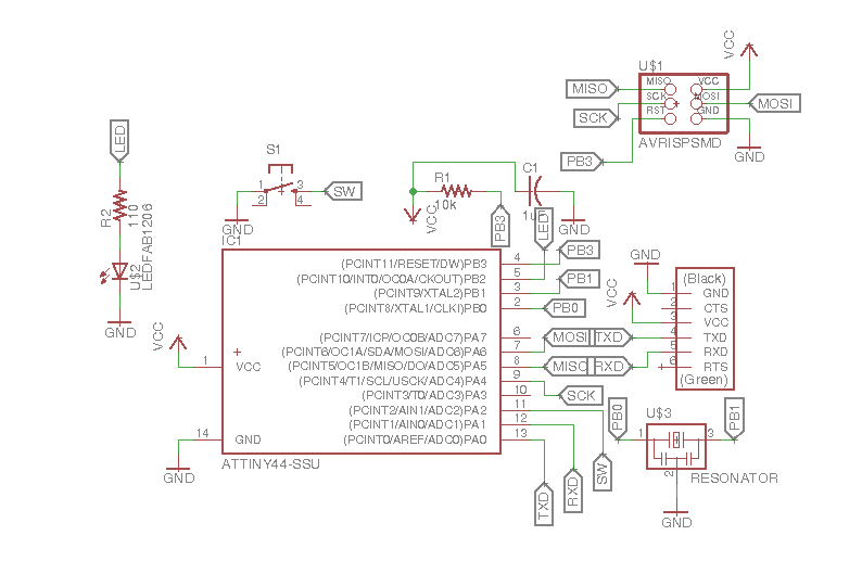
Now I start connecting the elements with each others. I use for that NET, NET is the line used to connect the elements. There are tow ways to connect the elements, either by drawing a line between the two elements or by using labels. The way to use labels are as follow. First we draw a line connect by one end to an element and floating on the other end, the we label the floating end. On the end where should the floating end should be connected, we do the same and label the other floating end with the same name. Now these two ends are connected to each others. In my design I have used label connections as much as possible. After including all the elements “including switch and LED”.
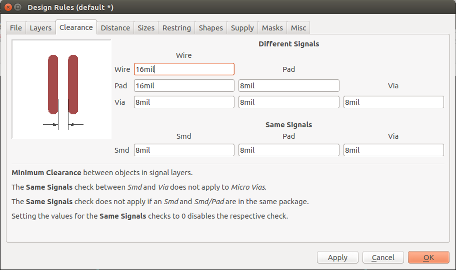
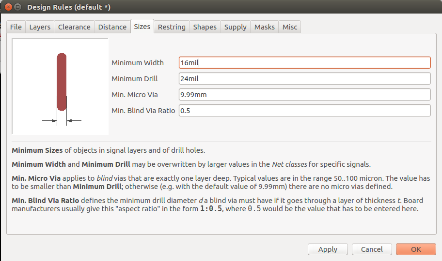
I click on BRD and view the new BRD design. I go to Edit → Design Rules → Clarence → Set wire and Pad to 16mil. Then go to Edit → Design Rules →Size → and set the path size to 16mil. Now click on Auto router → continue → start and eaglecad will start drawing multiple possible paths for the circuit board. Any 100% result means that all the outputs of the circuit board have been created successfully. If you have multiple 100% results. Then, it is better to choose one with less paths passing under the board elements. After finishing the board, Click on CAM processor Icon → File → open → Job and choose the downloaded file “cqw-gerb274x.cam” →Process Job. This will create a set of files CMP, SOL ...etc. SOL cam be used for both single side circuit board, or double side while CMP is used for single side Circuit Board :: Reference Link. . Now we take the CMP file and follow the same steps mentioned in week 4 “ Printing and Soldering the Circuit Board” :: Link. and we can check if the connection are correct by checking the Attiny44 pins with the 2x3 Header.
My Experience
My first struggle in week 6 was “how I am supposed to know the amount of resister required for the LED?”. The answer was as follow. Knowing that all I had to do simply OHM Laws was relaxing which is R = V/I → R = (Vc – Vf)/I. Now to get V and I is easy once you the trick. In this week I am installing an LED. So I went to download the data sheet of the LED. “whats the name of the LED?” I used the same name mentioned in the Schematic Design in EagleCad LED 1206. Luckily, the instructor saw this step and advised me take the details of the LED that we will be using in the LAB as LED 1206 is general. So I got the data sheet of the LED in our LAP :: Link.
Then I look for Voltage Forward and the required Current for the LED and run Ohms Law and get the resister value. R = (5 – 2.8)/20mA = 110 Ohm. But there is no 110 Ohm!. So using less resistance will burn the LED, Using Higher Resistance will have Low LED lighting. We had in the lap 100 Ohm and 330 Ohm. As 100 Ohm was quite close, I Chose it.
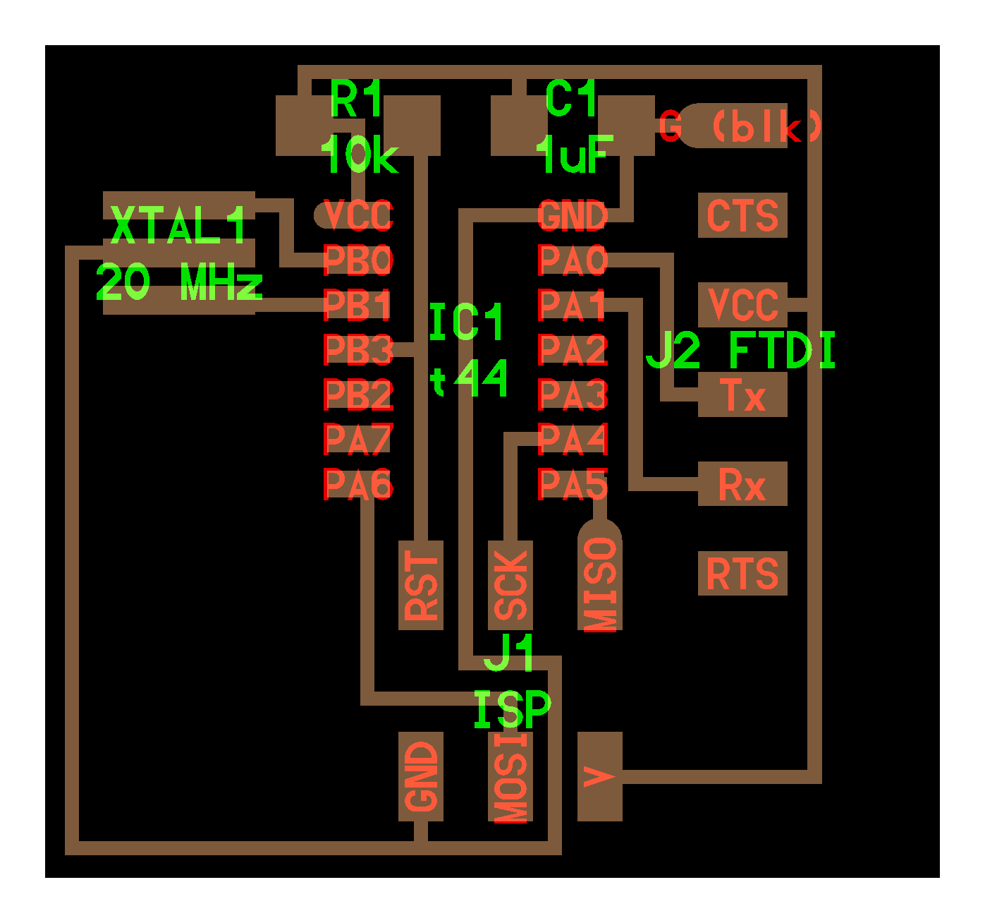
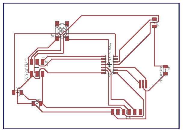
The second struggle was getting 100% out of the Auto routing in EagleCad. So basically I went to changing the location of the elements and rotating them, in a way to avoid intersection as much as possible till I came up with the following Circuit Board.
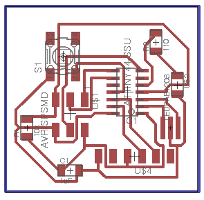
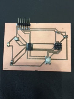
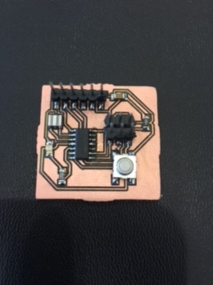
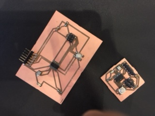
After printing and soldering the circuit board. I noticed that I had the baggiest Circuit Board in the class. So the third struggle was to print the smallest Circuit Board in the class. So I went again to BRD file with moving elements next to each other and Rotating & moving till the following result.
The Board Design
The following pictures shows the designs of the circuit boards, and the board sizes.
Milling and SolderingI fixed a copper board on the milling machine and followed the same process mentioned in detail in week 4 LINK TO WEEK 4 . After milling, I soldered the elements mentioned above in this document. Keeping in mind that I followed the Workflow and Area of improvement mentioned in the end of week 4 LINK TO WEEK 4 .
After Doing the soldering, I tested both boards to make sure that there is no Short circuit. First i made sure that AVR is connected to the correct pins in the Attiny 44. Then make sure that AVR pins are not connected to other pins. if every thing is fine. doing random checks would be nice to close this step.
Final Circuit Boards
Download Files
Schematic Design
Big Circuit Board
Small Circuit Board