Microcontroller Data Sheets
The first time I was going over the information on microcontrollers, I was lost like Alice in Wonderland, because I had not been familiar with microcontrollers at all before. I took notes on the basic information from ATtiny24A/44A/84A's and ATtiny25/45/85's datasheet, because I am planning to use ATtiny44A and ATtiny45 in the future course assignments and in the final project.
The most relevant information in the datasheets refers to the pin configurations, pin descriptions and alternate functions of the pins ports. This is the information I focused on when reading the datasheets.
ATtiny24A/44A/84A
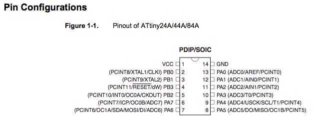
Pin Descriptions
- VCC - Supply voltage.
- GND - Ground.
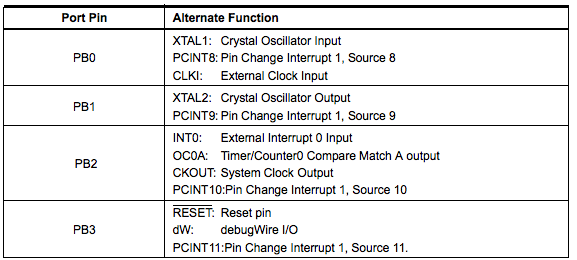
- Port B (PB3:PB0) - Port B is a 4-bit bi-directional I/O port with internal pull-up resistors (selected for each bit). The Port B output buffers have symmetrical drive characteristics with both high sink and source capability except PB3 which has the RESET capability. To use pin PB3 as an I/O pin, instead of RESET pin, program (‘0’) RSTDISBL fuse. As inputs, Port B pins that are externally pulled low will source current if the pull-up resistors are activated. The Port B pins are tri-stated when a reset condition becomes active, even if the clock is not running. Port B also serves the functions of various special features of the ATtiny24A/44A/84A.
- Port B, Bit 0 – XTAL1/PCINT8
XTAL1: Chip Clock Oscillator pin 1. Used for all chip clock sources except internal calibrateble RC oscillator. When used as a clock pin, the pin can not be used as an I/O pin. When using internal calibratable RC Oscillator as a chip clock source, PB0 serves as an ordinary I/O pin.
PCINT8: Pin Change Interrupt source 8. The PB0 pin can serve as an external interrupt source for pin change interrupt 1.
CLKI: Clock Input from an external clock source. - Port B, Bit 1 – XTAL2/PCINT9
XTAL2: Chip Clock Oscillator pin 2. Used as clock pin for all chip clock sources except internal calibrateble RC Oscillator and external clock. When used as a clock pin, the pin can not be used as an I/O pin. When using internal calibratable RC Oscillator or External clock as a Chip clock sources, PB1 serves as an ordinary I/O pin.
PCINT9: Pin Change Interrupt source 9. The PB1 pin can serve as an external interrupt source for pin change interrupt 1. - Port B, Bit 2 – INT0/OC0A/CKOUT/PCINT10
INT0: External Interrupt Request 0.
OC0A: Output Compare Match output: The PB2 pin can serve as an external output for the Timer/Counter0 Compare Match A. The PB2 pin has to be configured as an output (DDB2 set (one)) to serve this function. The OC0A pin is also the output pin for the PWM mode timer function.
CKOUT - System Clock Output: The system clock can be output on the PB2 pin. The system clock will be output if the CKOUT Fuse is programmed, regardless of the PORTB2 and DDB2 settings. It will also be output during reset.
PCINT10: Pin Change Interrupt source 10. The PB2 pin can serve as an external interrupt source for pin change interrupt 1. - Port B, Bit 3 – RESET/dW/PCINT11
RESET: External Reset input is active low and enabled by unprogramming (“1”) the RSTDISBL Fuse. Pullup is activated and output driver and digital input are deactivated when the pin is used as the RESET pin.
dW: When the debugWIRE Enable (DWEN) Fuse is programmed and Lock bits are unprogrammed, the debugWIRE system within the target device is activated. The RESET port pin is configured as a wire-AND (open-drain) bi-directional I/O pin with pull-up enabled and becomes the communication gateway between target and emulator.
PCINT11: Pin Change Interrupt source 11. The PB3 pin can serve as an external interrupt source for pin change interrupt 1. - RESET - Reset input. A low level on this pin for longer than the minimum pulse length will generate a reset, even if the clock is not running and provided the reset pin has not been disabled. The minimum pulse length is given in Table 20-4 on page 176. Shorter pulses are not guaranteed to generate a reset. The reset pin can also be used as a (weak) I/O pin.
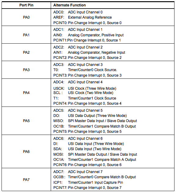
- Port A (PA7:PA0) - Port A is a 8-bit bi-directional I/O port with internal pull-up resistors (selected for each bit). The Port A output buffers have symmetrical drive characteristics with both high sink and source capability. As inputs, Port A pins that are externally pulled low will source current if the pull-up resistors are activated. The Port A pins are tri-stated when a reset condition becomes active, even if the clock is not running. Port A has alternate functions as analog inputs for the ADC, analog comparator, timer/counter, SPI and pin change interrupt.
- Port A, Bit 0 – ADC0/AREF/PCINT0
ADC0: Analog to Digital Converter, Channel 0.
AREF: External Analog Reference for ADC. Pullup and output driver are disabled on PA0 when the pin is used as an external reference or Internal Voltage Reference with external capacitor at the AREF pin by setting (one) the bit REFS0 in the ADC Multiplexer Selection Register (ADMUX).
PCINT0: Pin Change Interrupt source 0. The PA0 pin can serve as an external interrupt source for pin change interrupt 0. - Port A, Bit 1 – ADC1/AIN0/PCINT1
ADC1: Analog to Digital Converter, Channel 1.
AIN0: Analog Comparator Positive Input. Configure the port pin as input with the internal pullup switched off to avoid the digital port function from interfering with the function of the Analog Comparator.
PCINT1: Pin Change Interrupt source 1. The PA1 pin can serve as an external interrupt source for pin change interrupt 0. - Port A, Bit 2 – ADC2/AIN1/PCINT2
ADC2: Analog to Digital Converter, Channel 2.
AIN1: Analog Comparator Negative Input. Configure the port pin as input with the internal pull-up switched off to avoid the digital port function from interfering with the function of the Analog Comparator.
PCINT2: Pin Change Interrupt source 2. The PA2 pin can serve as an external interrupt source for pin change interrupt 0. - Port A, Bit 3 – ADC3/T0/PCINT3
ADC3: Analog to Digital Converter, Channel 3.
T0: Timer/Counter0 counter source.
PCINT3: Pin Change Interrupt source 3. The PA3 pin can serve as an external interrupt source for pin change interrupt 0. - Port A, Bit 4 – ADC4/USCK/SCL/T1/PCINT4
ADC4: Analog to Digital Converter, Channel 4.
USCK: Three-wire mode Universal Serial Interface Clock.
SCL: Two-wire mode Serial Clock for USI Two-wire mode.
T1: Timer/Counter1 counter source.
PCINT4: Pin Change Interrupt source 4. The PA4 pin can serve as an external interrupt source for pin change interrupt 0. - Port A, Bit 5 – ADC5/DO/MISO/OC1B/PCINT5
ADC5: Analog to Digital Converter, Channel 5.
DO: Data Output in USI Three-wire mode. Data output (DO) overrides PORTA5 value and it is driven to the port when the data direction bit DDA5 is set (one). However the PORTA5 bit still controls the pullup, enabling pullup if direction is input and PORTA5 is set(one).
MISO: Master Data input, Slave Data output pin for SPI channel. When the SPI is enabled as a Master, this pin is configured as an input regardless of the setting of DDA5. When the SPI is enabled as a Slave, the data direction of this pin is controlled by DDA5. When the pin is forced by the SPI to be an input, the pull-up can still be controlled by the PORTA5 bit.
OC1B: Output Compare Match output: The PA5 pin can serve as an external output for the Timer/Counter1 Compare Match B. The PA5 pin has to be configured as an output (DDA5 set (one)) to serve this function. The OC1B pin is also the output pin for the PWM mode timer function.
PCINT5: Pin Change Interrupt source 5. The PA5 pin can serve as an external interrupt source for pin change interrupt 0. - Port A, Bit 6 – ADC6/DI/SDA/MOSI/OC1A/PCINT6
ADC6: Analog to Digital Converter, Channel 6.
SDA: Two-wire mode Serial Interface Data.
DI: Data Input in USI Three-wire mode. USI Three-wire mode does not override normal port functions, so pin must be configure as an input for DI function.
MOSI: Master Data output, Slave Data input for SPI channel. When the SPI is enabled as a Slave, this pin is configured as an input regardless of the setting of DDA6. When the SPI is enabled as a Master, the data direction of this pin is controlled by DDA6. When the pin is forced by the SPI to be an input, the pull-up can still be controlled by the PORTA6 bit.
OC1A, Output Compare Match output: The PA6 pin can serve as an external output for the Timer/Counter1 Compare Match A. The pin has to be configured as an output (DDA6 set (one)) to serve this function. This is also the output pin for the PWM mode timer function.
PCINT6: Pin Change Interrupt source 6. The PA6 pin can serve as an external interrupt source for pin change interrupt 0. - Port A, Bit 7 – ADC7/OC0B/ICP1/PCINT7
ADC7: Analog to Digital Converter, Channel 7.
OC1B, Output Compare Match output: The PA7 pin can serve as an external output for the Timer/Counter1 Compare Match B. The pin has to be configured as an output (DDA7 set (one)) to serve this function. This is also the output pin for the PWM mode timer function.
ICP1, Input Capture Pin: The PA7 pin can act as an Input Capture Pin for Timer/Counter1.
PCINT7: Pin Change Interrupt source 7. The PA7 pin can serve as an external interrupt source for pin change interrupt 0.
ATtiny25/45/85
Pin Descriptions
- VCC - Supply voltage.
- GND - Ground.
- Port B (PB5:PB0) - Port B is a 6-bit bi-directional I/O port with internal pull-up resistors (selected for each bit). The Port B output buffers have symmetrical drive characteristics with both high sink and source capability. As inputs, Port B pins that are externally pulled low will source current if the pull-up resistors are activated. The Port B pins are tri-stated when a reset condition becomes active, even if the clock is not running. Port B also serves the functions of various special features of the ATtiny25/45/85.
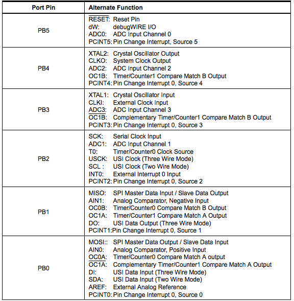
- Port B, Bit 5 – RESET/dW/ADC0/PCINT5
RESET: External Reset input is active low and enabled by unprogramming (“1”) the RSTDISBL Fuse. Pullup is activated and output driver and digital input are deactivated when the pin is used as the RESET pin.
dW: When the debugWIRE Enable (DWEN) Fuse is programmed and Lock bits are unprogrammed, the debugWIRE system within the target device is activated. The RESET port pin is configured as a wire-AND (open-drain) bi-directional I/O pin with pull-up enabled and becomes the communication gateway between target and emulator.
ADC0: Analog to Digital Converter, Channel 0.
PCINT5: Pin Change Interrupt source 5. - Port B, Bit 4 – XTAL2/CLKO/ADC2/OC1B/PCINT4
XTAL2: Chip Clock Oscillator pin 2. Used as clock pin for all chip clock sources except internal calibrateble RC Oscillator and external clock. When used as a clock pin, the pin can not be used as an I/O pin. When using internal calibratable RC Oscillator or External clock as a Chip clock sources, PB4 serves as an ordinary I/O pin.
CLKO: The devided system clock can be output on the pin PB4. The divided system clock will be output if the CKOUT Fuse is programmed, regardless of the PORTB4 and DDB4 settings. It will also be output during reset.
ADC2: Analog to Digital Converter, Channel 2.
OC1B: Output Compare Match output: The PB4 pin can serve as an external output for the Timer/Counter1 Compare Match B when configured as an output (DDB4 set). The OC1B pin is also the output pin for the PWM mode timer function.
PCINT4: Pin Change Interrupt source 4. - Port B, Bit 3 – XTAL1/CLKI/ADC3/OC1B/PCINT3
XTAL1: Chip Clock Oscillator pin 1. Used for all chip clock sources except internal calibrateble RC oscillator. When used as a clock pin, the pin can not be used as an I/O pin.
CLKI: Clock Input from an external clock source.
ADC3: Analog to Digital Converter, Channel 3.
OC1B: Inverted Output Compare Match output: The PB3 pin can serve as an external output for the Timer/Counter1 Compare Match B when configured as an output (DDB3 set). The OC1B pin is also the inverted output pin for the PWM mode timer function.
PCINT3: Pin Change Interrupt source 3. - Port B, Bit 2 – SCK/ADC1/T0/USCK/SCL/INT0/PCINT2
SCK: Master Clock output, Slave Clock input pin for SPI channel. When the SPI is enabled as a Slave, this pin is configured as an input regardless of the setting of DDB2. When the SPI is enabled as a Master, the data direction of this pin is controlled by DDPB2. When the pin is forced by the SPI to be an input, the pull-up can still be controlled by the PORTB2 bit.
ADC1: Analog to Digital Converter, Channel 1.
T0: Timer/Counter0 counter source.
USCK: Three-wire mode Universal Serial Interface Clock.
SCL: Two-wire mode Serial Clock for USI Two-wire mode.
INT0: External Interrupt source 0.
PCINT2: Pin Change Interrupt source 2. - Port B, Bit 1 – MISO/AIN1/OC0B/OC1A/DO/PCINT1
MISO: Master Data input, Slave Data output pin for SPI channel. When the SPI is enabled as a Master, this pin is configured as an input regardless of the setting of DDB1. When the SPI is enabled as a Slave, the data direction of this pin is controlled by DDB1. When the pin is forced by the SPI to be an input, the pull-up can still be controlled by the PORTB1 bit.
AIN1: Analog Comparator Negative Input. Configure the port pin as input with the internal pull-up switched off to avoid the digital port function from interfering with the function of the Analog Comparator.
OC0B: Output Compare Match output. The PB1 pin can serve as an external output for the Timer/Counter0 Compare Match B. The PB1 pin has to be configured as an output (DDB1 set (one)) to serve this function. The OC0B pin is also the output pin for the PWM mode timer function.
OC1A: Output Compare Match output: The PB1 pin can serve as an external output for the Timer/Counter1 Compare Match B when configured as an output (DDB1 set). The OC1A pin is also the output pin for the PWM mode timer function.
DO: Three-wire mode Universal Serial Interface Data output. Three-wire mode Data output overrides PORTB1 value and it is driven to the port when data direction bit DDB1 is set (one). PORTB1 still enables the pull-up, if the direction is input and PORTB1 is set (one).
PCINT1: Pin Change Interrupt source 1. - Port B, Bit 0 – MOSI/AIN0/OC0A/OC1A/DI/SDA/AREF/PCINT0
MOSI: SPI Master Data output, Slave Data input for SPI channel. When the SPI is enabled as a Slave, this pin is configured as an input regardless of the setting of DDB0. When the SPI is enabled as a Master, the data direction of this pin is controlled by DDB0. When the pin is forced by the SPI to be an input, the pull-up can still be controlled by the PORTB0 bit.
AIN0: Analog Comparator Positive Input. Configure the port pin as input with the internal pull-up switched off to avoid the digital port function from interfering with the function of the Analog Comparator.
OC0A: Output Compare Match output. The PB0 pin can serve as an external output for the Timer/Counter0 Compare Match A when configured as an output (DDB0 set (one)). The OC0A pin is also the output pin for the PWM mode timer function.
OC1A: Inverted Output Compare Match output: The PB0 pin can serve as an external output for the Timer/Counter1 Compare Match B when configured as an output (DDB0 set). The OC1A pin is also the inverted output pin for the PWM mode timer function.
SDA: Two-wire mode Serial Interface Data.
AREF: External Analog Reference for ADC. Pullup and output driver are disabled on PB0 when the pin is used as an external reference or Internal Voltage Reference with external capacitor at the AREF pin.
DI: Data Input in USI Three-wire mode. USI Three-wire mode does not override normal port functions, so pin must be configure as an input for DI function.
PCINT0: Pin Change Interrupt source 0.
On ATtiny25, the programmable I/O ports PB3 and PB4 (pins 2 and 3) are exchanged in ATtiny15 Compatibility Mode for supporting the backward compatibility with ATtiny15. - Port B, Bit 5 – RESET/dW/ADC0/PCINT5
- RESET - Reset input. A low level on this pin for longer than the minimum pulse length will generate a reset, even if the clock is not running and provided the reset pin has not been disabled. The minimum pulse length is given in Table 21-4 on page 165 of the datasheet. Shorter pulses are not guaranteed to generate a reset. The reset pin can also be used as a (weak) I/O pin.
After learning the basics, I have a better idea of how microcontrollers are set up. In the future, I would like to focus more on the code examples sections of the datasheets to understand better how to program microcontrollers.
Programming the board
Preparation
A good place to start with is prepare necessary hardware and software for completing the assignment. Required hardware is:
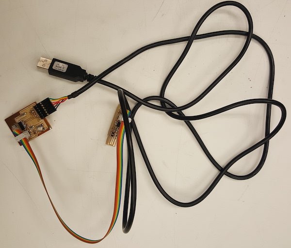
I used Windows 10 OS, avrdude, Atmel Studio, and Arduino IDE to program my board. For additional guidelines, I referred to documentation of Fab Lab Oulu 2016 graduates: Antti, Dorina, and Juha. I installed
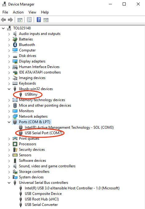
If all drivers are installed, the Device Manager recognizes the USBTiny and the FTDI cable
Atmel Studio
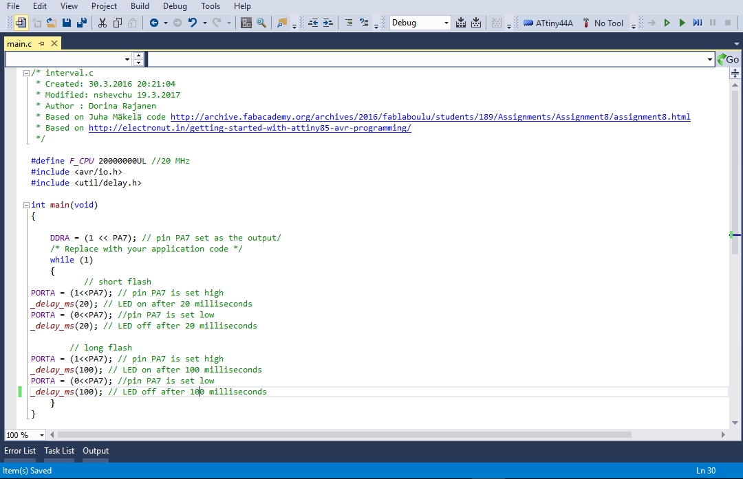
I created two projects in Atmel Studio. I used modified program codes. To create the hello project:
File - New - Project
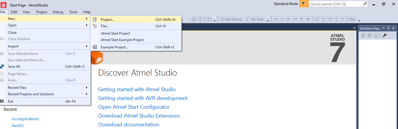
GCC C Executable Project-Name:hello - OK
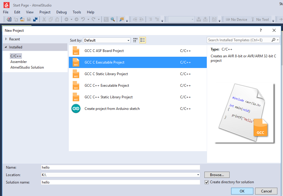
Device Selection - ATtiny44A - OK

Build - Compile
Build - Build Solution
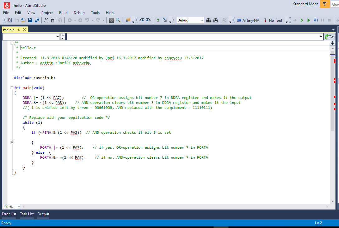
After that, I located hello.hex file in the Debug folder of the hello application, copied and pasted it to the avrdude folder for the further steps. Similarly, I created the interval project.
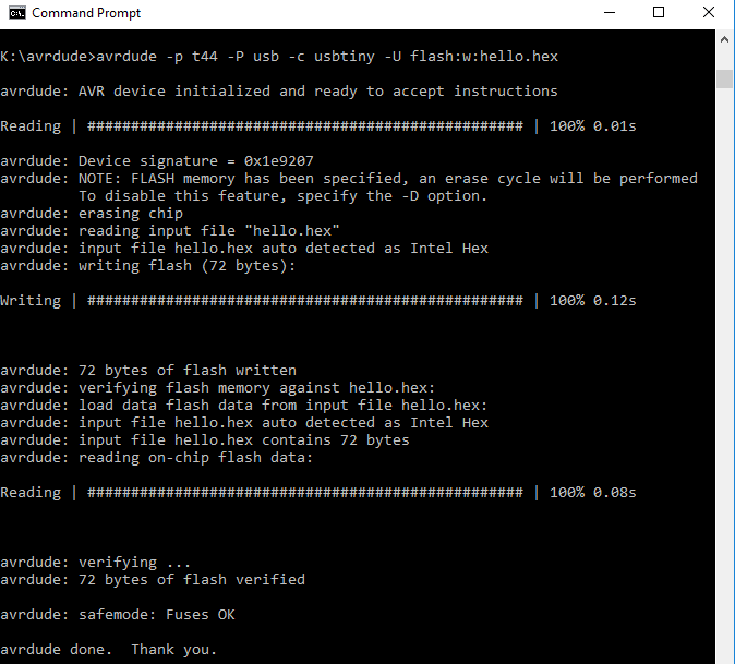
avrdude
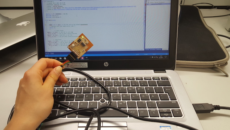
At this point, the USBTiny, to-be-programmed board, and the FTDI cable have to be connected. Avrdure can be opened in command line.
avrdude -p t44 -P usb -c usbtiny -U flash:w:hello.hex
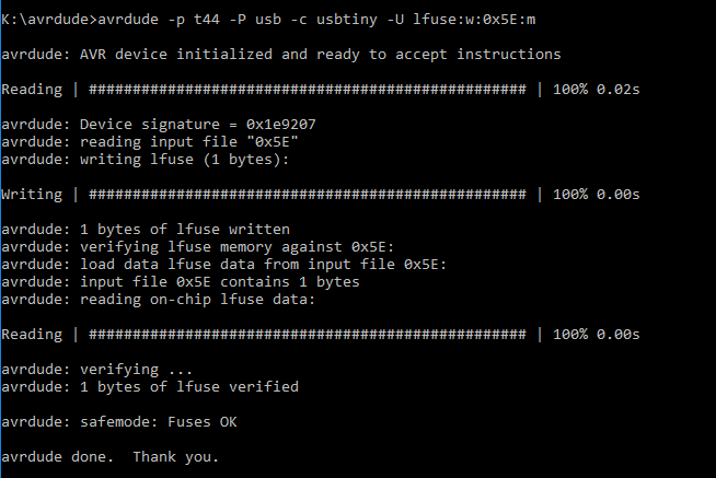
Checking settings for ATtiny44A fuses can be done at engbedded.com.
avrdude -p t44 -P usb -c usbtiny -U lfuse:w:0x5E:m
Initially, I kept getting the "avrdude: initialization failed, rc=-1" error.
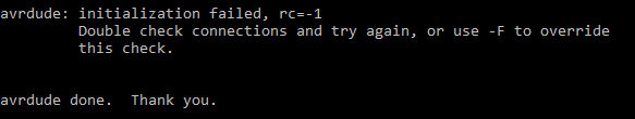
I used Laia Mogas-Soldevila's checklist to find and fix the problem:
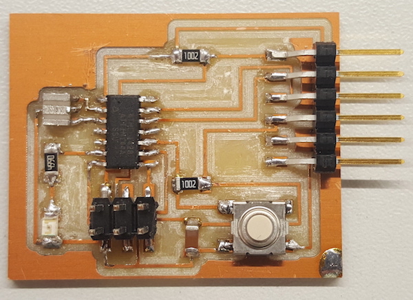
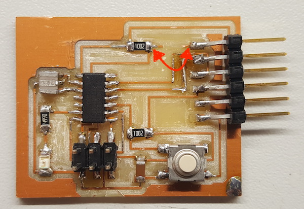
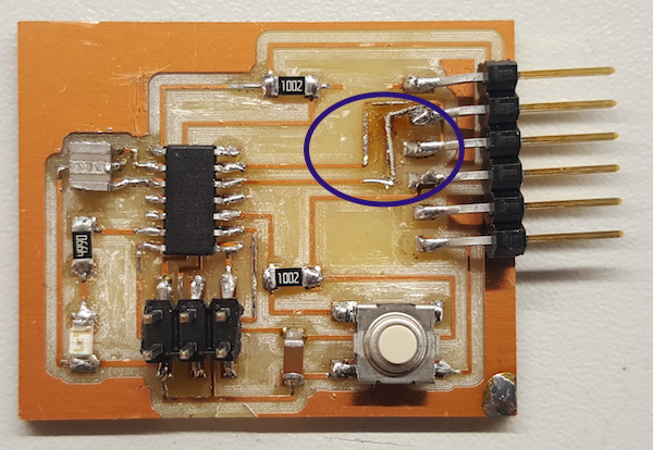
I finally discovered that the error was caused by an extra connection on my board. The error was eliminated after the connection was cut. See Hardware Issues below.
Arduino IDE
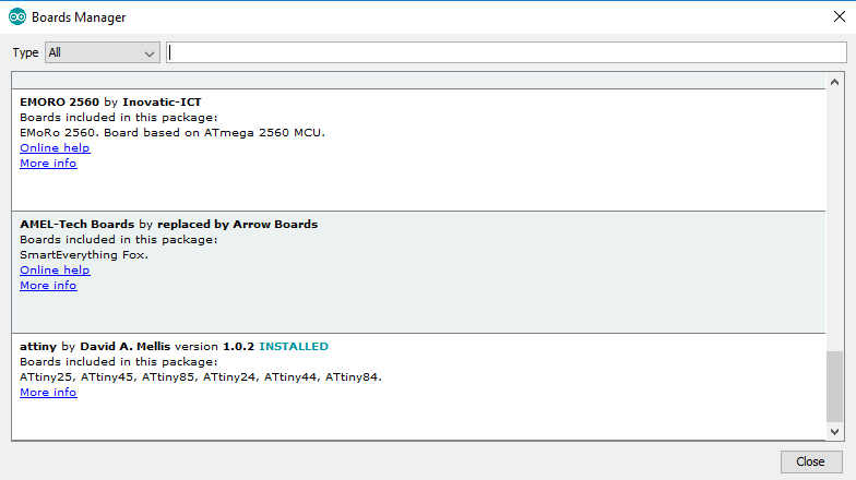
To install ATtiny in Arduino, I used Highlowtech guide and Antti's documentation.
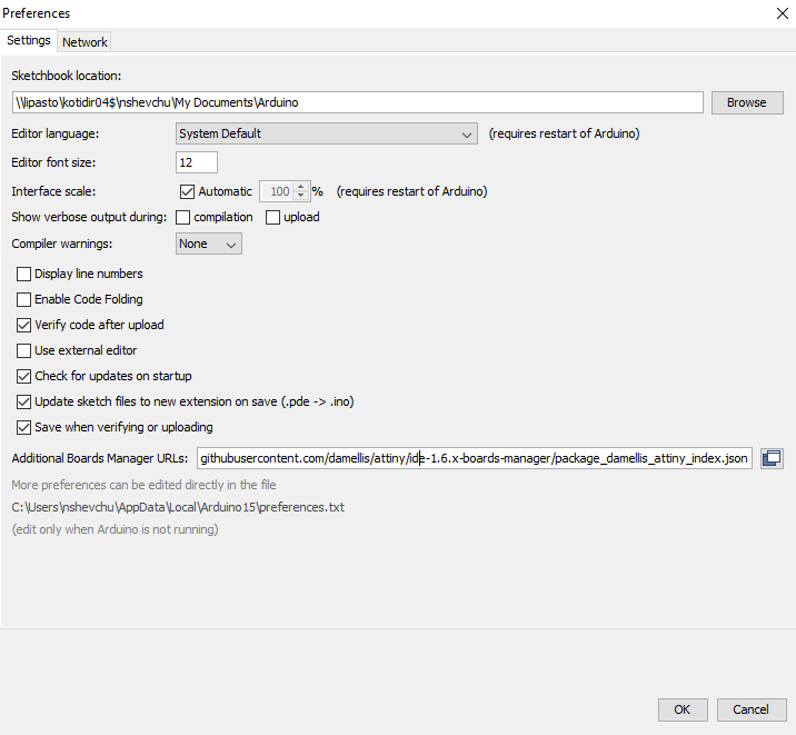
File - Preferences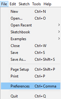

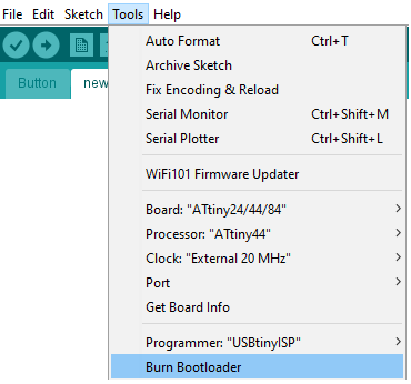
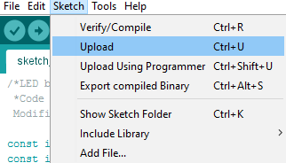
I was able to program my board with the example codes. Sketch - Upload, or the Upload button can be used for programming the board
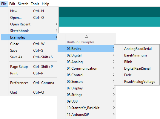
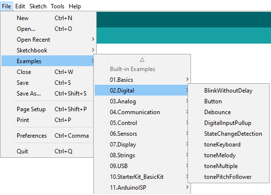
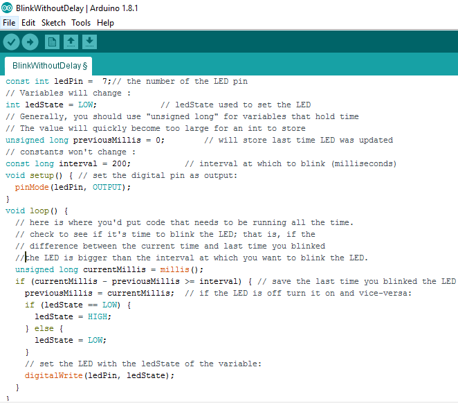
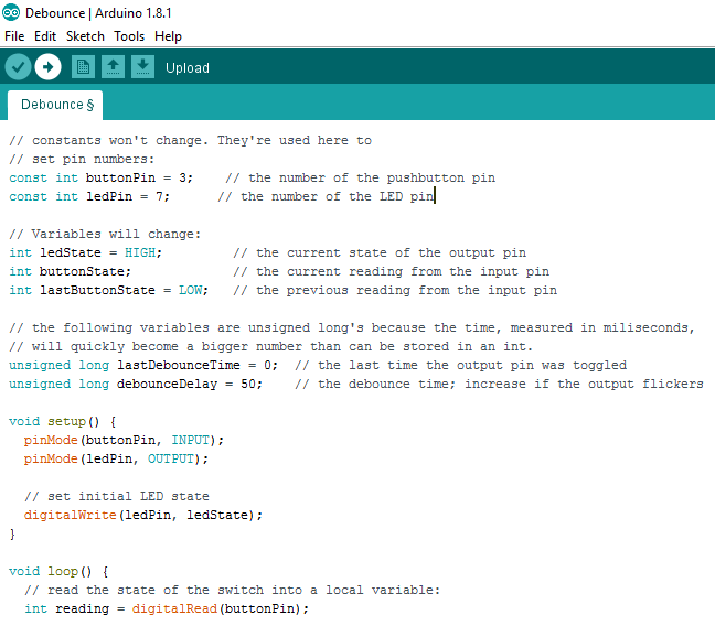
File - Examples - 01.Basics
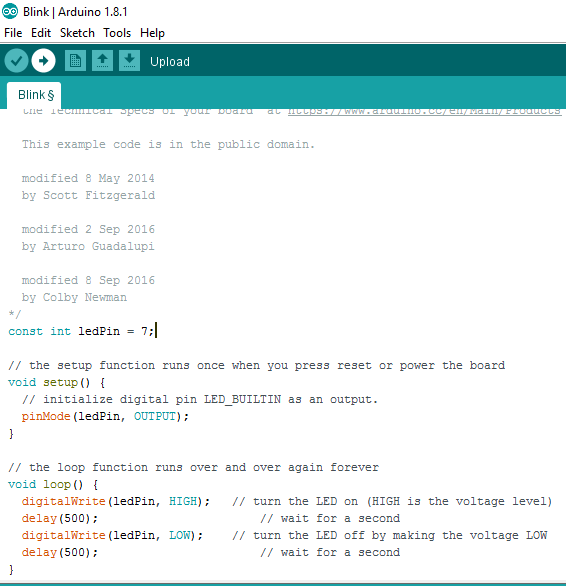
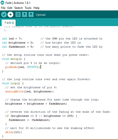
I changed delay from 30 to 10 miliseconds.
File - Examples - 02.Digital
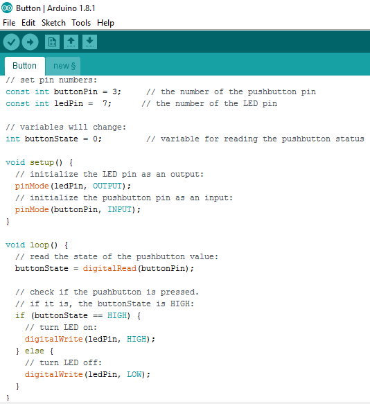
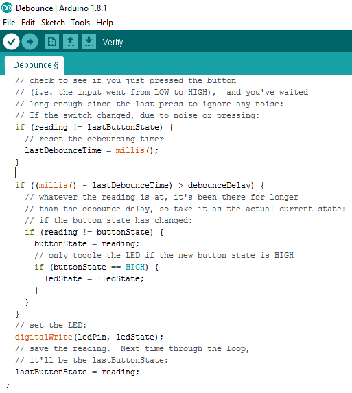
as well as the LED-Button code by Charlie Banthrope modified to my board design ("DiffBlinking").
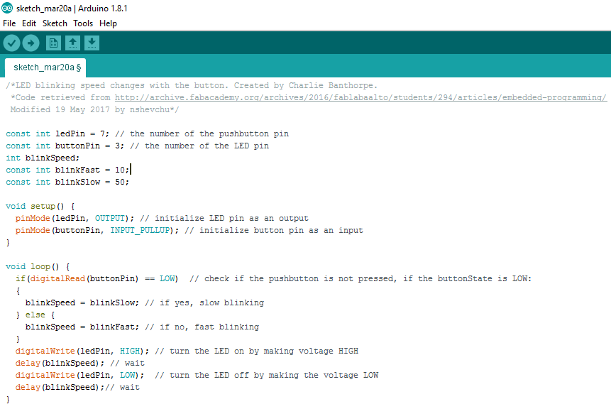
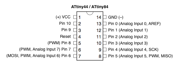
I changed pins' numbers in these codes. For the pins reference, I referred to the diagram at Highlowtech guide.
Hardware Issues
After receiving a repetitive connection error in avrdude, I revisited my design and I noticed an error in schematic layout. Because of this error, I ended up having an extra connection, which apparently was preventing the board from being programmed. After I cut the connection, the programmer and the board were able to communicate.
I went back to the instructions I used for the week 6 assignment, and found that the sample schematic I recreated referring to (Example Schematic with LED and button added with appropiate resistors and connections to power and ground) returns errors.
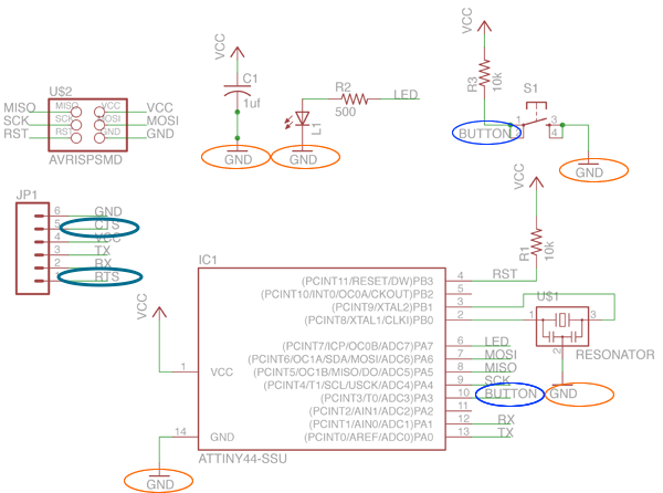
Since I was following the guide, I had to update my layout in Eagle to make it error-free.
Another problem I ran into this week was damaging traces on the board. After being used for a while, the FTDI header disattached from the board and one of the traces broke. With an extra piece of wire and resoldering the component, I was able to bring the board back to life.
Files:
Hello and Interval program .c and .hex files, Blink, Fade, BlinkWithoutDelay, Button, Debounce .ino Arduino files
Remember, remember...
- Refer to the datasheet regualrly to understand completely and fullt utilize its functionality
- Carefully check hardware design. It is likely that most of your programming errors will occur due to issues with hardware
- "Error 1" for "avrdude: initialization failed, rc=-1 Double check connections and try again" is one of the most common and happens most often because of hardware issues, be prepared dealing with it
- For the beginners, it is good to get started with the sample codes, which have been tested before. This will help confirming that the issues are due to hardware mistakes
- When the hardware is definitely functional, move on to more complicated examples.