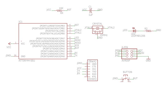
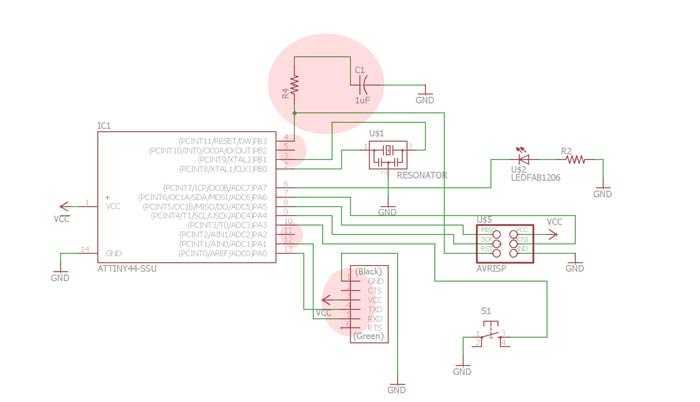
This weeks task was to redraw the circuit we worked on during the Electronics Production week and add input / output parts to it.
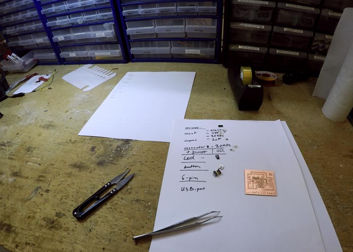
The components I will use are:- a microcontroller (ATtiny-44)
- resistors (10KΩ, 499Ω)
- capacitors (1μF)
- resonator (20ΜΗz)
- 6-pin header (AVRISPsmd)
- USB port
- a button / switches (input), and
- a LED (output). All components are surface mount.
The first thing to do was to get familiar with Eagle, the electronics design software.
Following this tutorial made it possible to build the circuit starting from scratch.
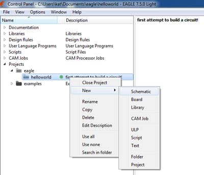
Starting with the new project, I loaded the FabLab Component Library on Eagle in order to add the right components for the schematic. Following the instructions, I tried to reproduce the schematic of the circuit. The next thing to do was to add the button and the LED and wire them correctly, using resistors to connect them to the microcontroller.
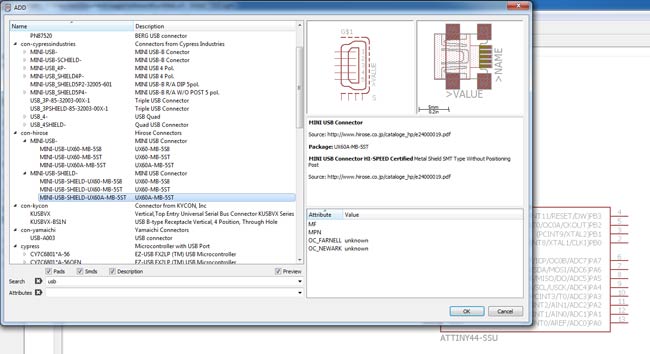
I started importing the pieces.
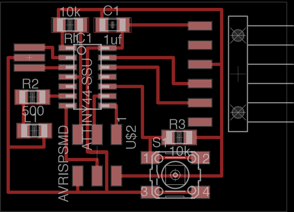
Designing the Board Layout, making the traces to connect the components from the schematic view, required finding the right way to place the already connected components on the space of the board. In the tutorial the was already a design solution proposed, but I decided to find my own way to design the traces, so that I get to understand more about solving the connections, moving the parts around and creating the space on the board.
In order to make it work, I had to add a 0Ω resistor as a jumper to my circuit. First I loaded the component to my Eagle schematic. When I found exactly how to place it in the circuit, I returned to the schematic and connected it with the rest of my components so that it become part of my circuit connected with the air wires on my board layout.
The red dots are showing the first problems I got in the process. Because this was the first board I was making I had some connections taht were wrong. Those problems are carefully explained in Week 8: Embedded programming.
The next step waas switching from the schematic view to the board view. This view can be tricky, first you need to place the components close and in a way that makes you easy to wire them. So there is a lot of back and forth operations involved until you get the right position with NO overlapping connections.
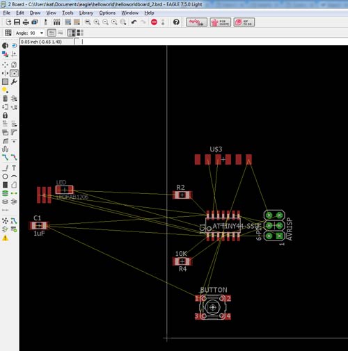
Because was the first some errors are present, like the button component you can see in the next picture. But those were fixed along the next steps.
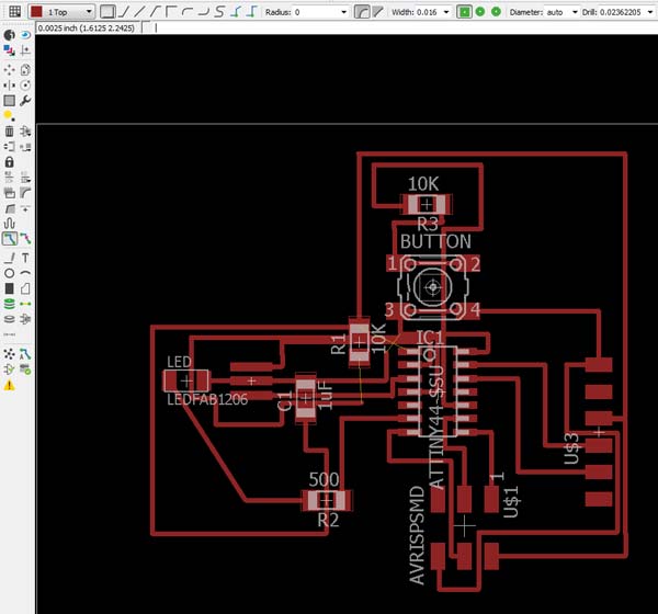
I added this dotted line and is named GND in order to connect the GND parts of the board, as I saw in the tutorial I saw. but this is something I wouldn't recommend if is not needed, because makes soldering process a lot more difficult.
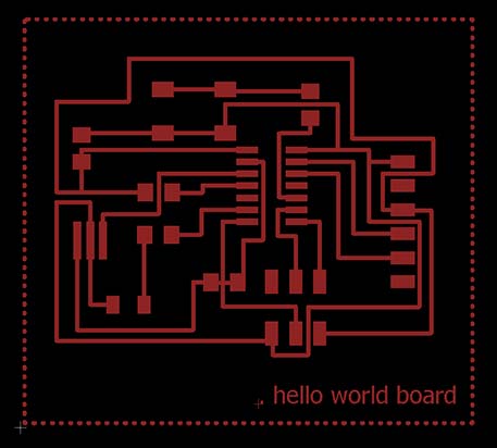
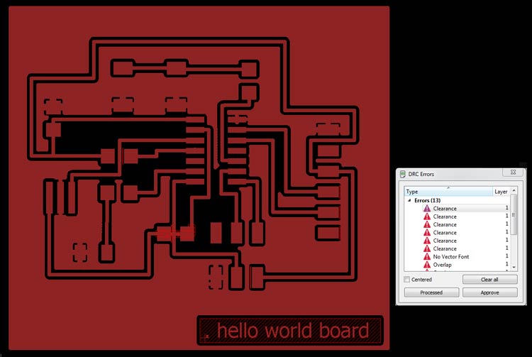
This is how we pass from one design to the other. And after finishing the board I did the command DRC (Design Rule Check), for checking the clearence. And as you can see I had some clearence problems, that I corrected changing the distance for the gap.
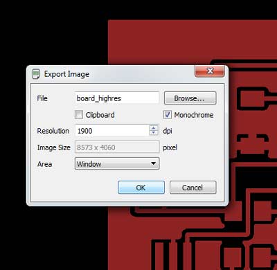
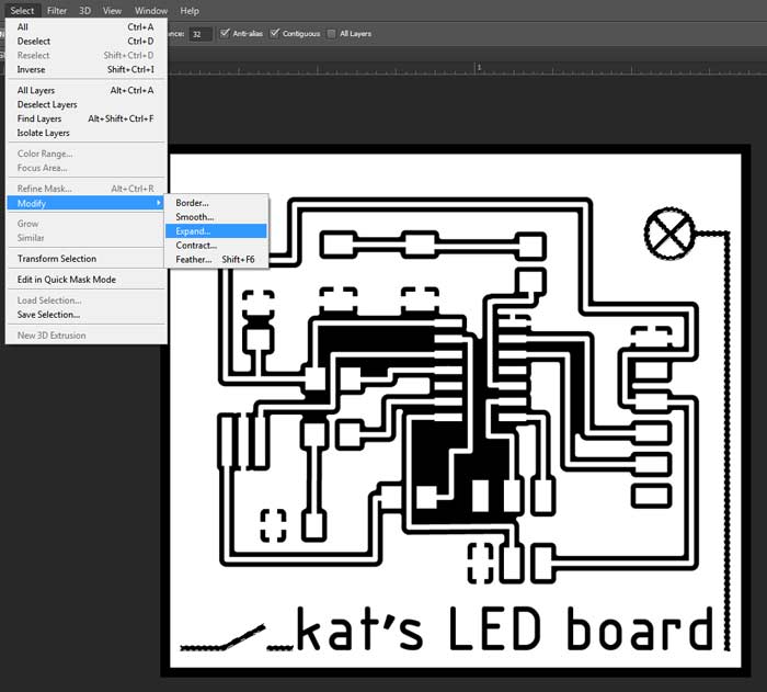
The next step was to export the .png files in monochrome and the window area, I set a very high resolution 1900 dpi, when with a lower one, something between 500 and 600 dpi is enough.
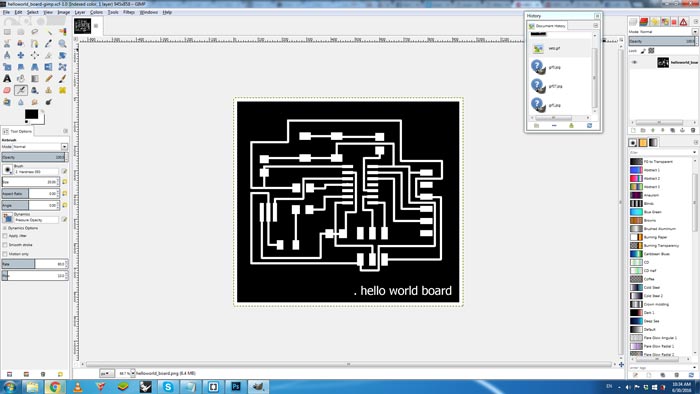
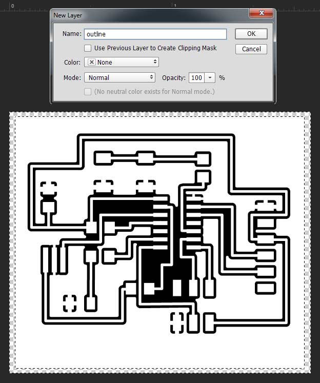
I used Gimp for editing the .png, but I was a mess. I'm used to Photoshop, so after a while trying I jumped to Photoshop and prepared the .png for the Fabmodules: I prepared two files, the traces and the outline.
Milling & Soldering the board
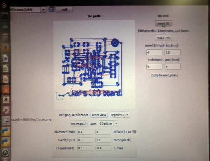
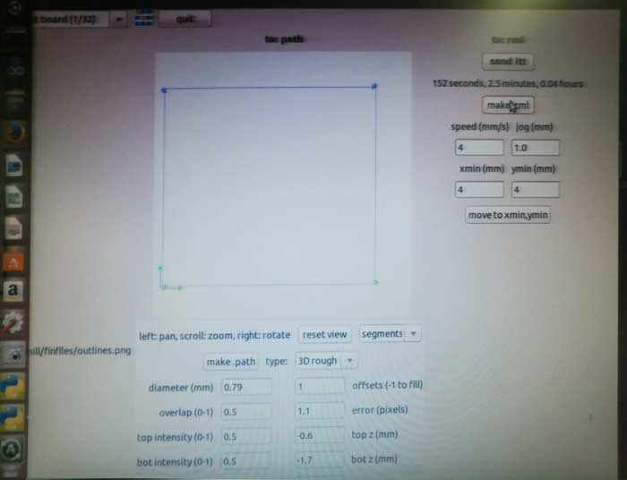
Preparing for Milling with the Roland SRM20, I used Fabmodules, from a Linux computer. In the next picture you can see the settings for the milling.
For the traces (first to mill), we use a 1/64 milling bit.
For the outline (cutting the board), we use a 1/32 milling bit.
Fabmodules has specific process that we need to choose (with the name 1/64 and 1/32) depending on the process we want to execute.
Settings for process 1/64 (milling the traces).
Setting for the 1/32 (milling the outline).
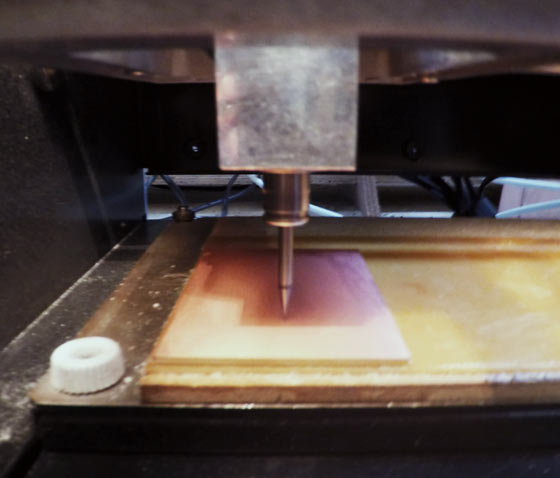
The next image shows the Roland SRM20 at the beginning of the milling process.
The next step is to prepare for stuffing the board. First write down the bill of materials, then look for the componenets and finally solder them in the right place. You have to look at your design in the computer to know the right place, and check if the component have a specific position.
Components such as diodes (LED), microcontrollers (AtTiny 44) and buttons have a specific direction to be soldered.
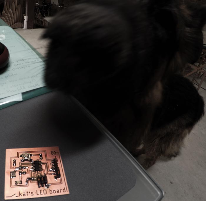
My Hello-World board after soldering!
The .png files for my final board can be found here. I include the troubleshooted Eagle schematic and board file.
Troubleshooting and making the board work is documented in the Embedded Programming (Week 8) assignment.