Assignments:
- Redraw the echo hello-world board  and add at least a button and LED for free pins.
- Check the design rules, make it, and test it
Warming up with Eagle
1. Download fab.lbr file, rename it "00fab.lbr"(you will see why). Move it to C: Eagle folder(Eagle 8.0.2)>library folder(lbr)
2. File>New>Project
3. New>Schematic
4.(On SCH(schematic page)) library>use>00fab.
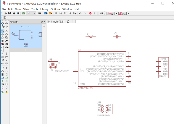
5. Click add icon. From 00fab library, choose proper components(with the same name, same functionality, they might be different), and display them.
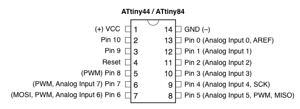
6. For now: Attiny44>Attiny44-SSU (vcc-circle) / AVRISP>AVRISPSMD(6pin ISP) / Cap-unpolarized>Cap-unpolarized C1206 / FTDI-SMD-header / Res-US>Res-US1206 / Resonator(crystal:middle should be connected to GND)
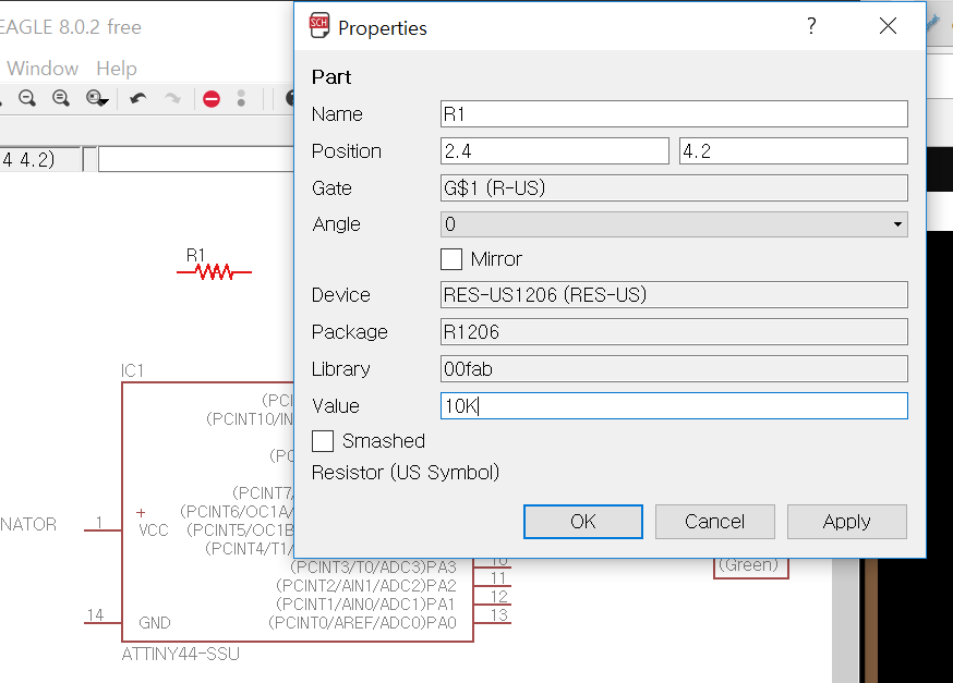
(Res, Cap: can put values by clicking (i)-information icon, and then the component==>put values)
7. click the button to get the layout page.
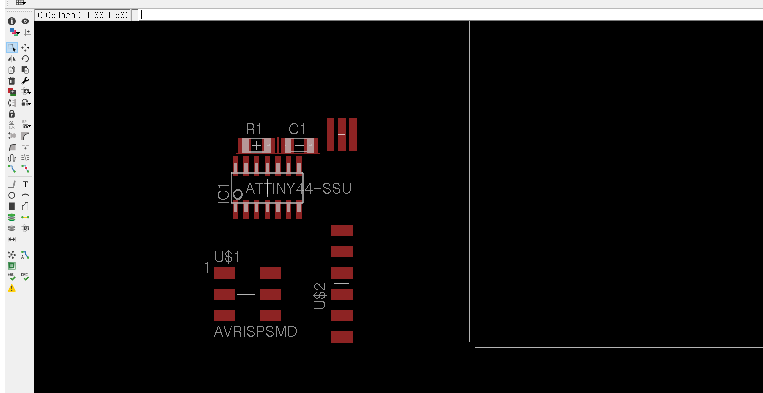
8. (On BRD(layout page)) move them into the white rectangular boundary,'Dimension'. (When you need to move objects, click + sign inside the object, and drag it.)
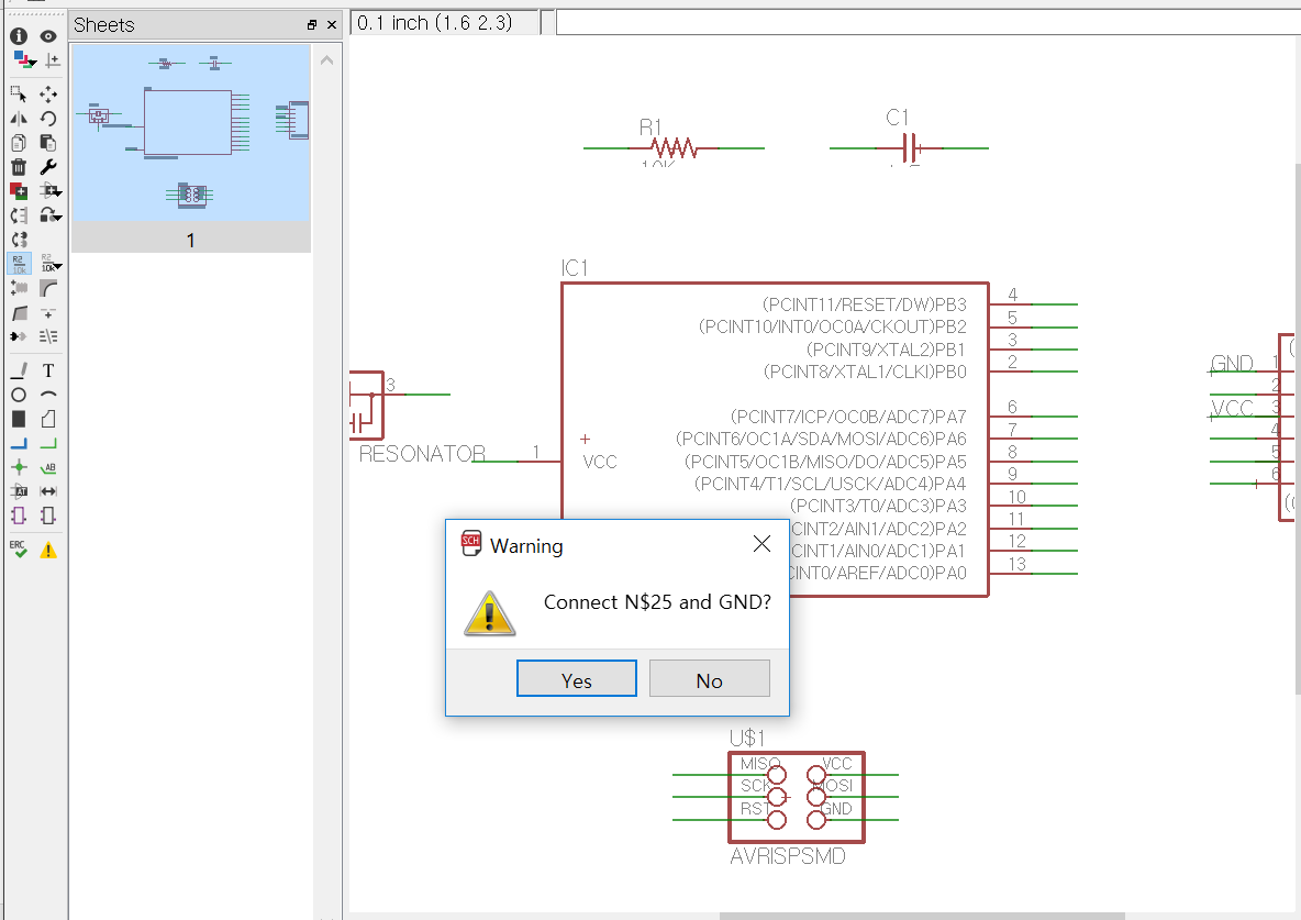
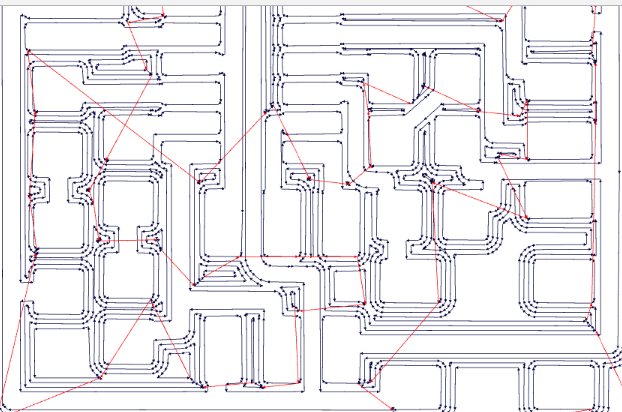
9. (On SCH)You can either draw all the lines connecting components, or draw only short lines from each components, and by labelling proper names, you can connect two or more components behind the scene. (Say yes to this if you really want them to be connected!)
10. (On BRD)You can see the connections in yellow line.
11. Draw route for those connections. Consider other connections that are not shown yet:
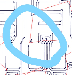
At first, I connected like this, but...
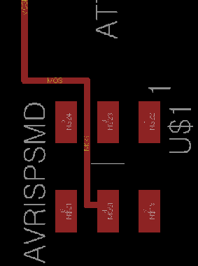
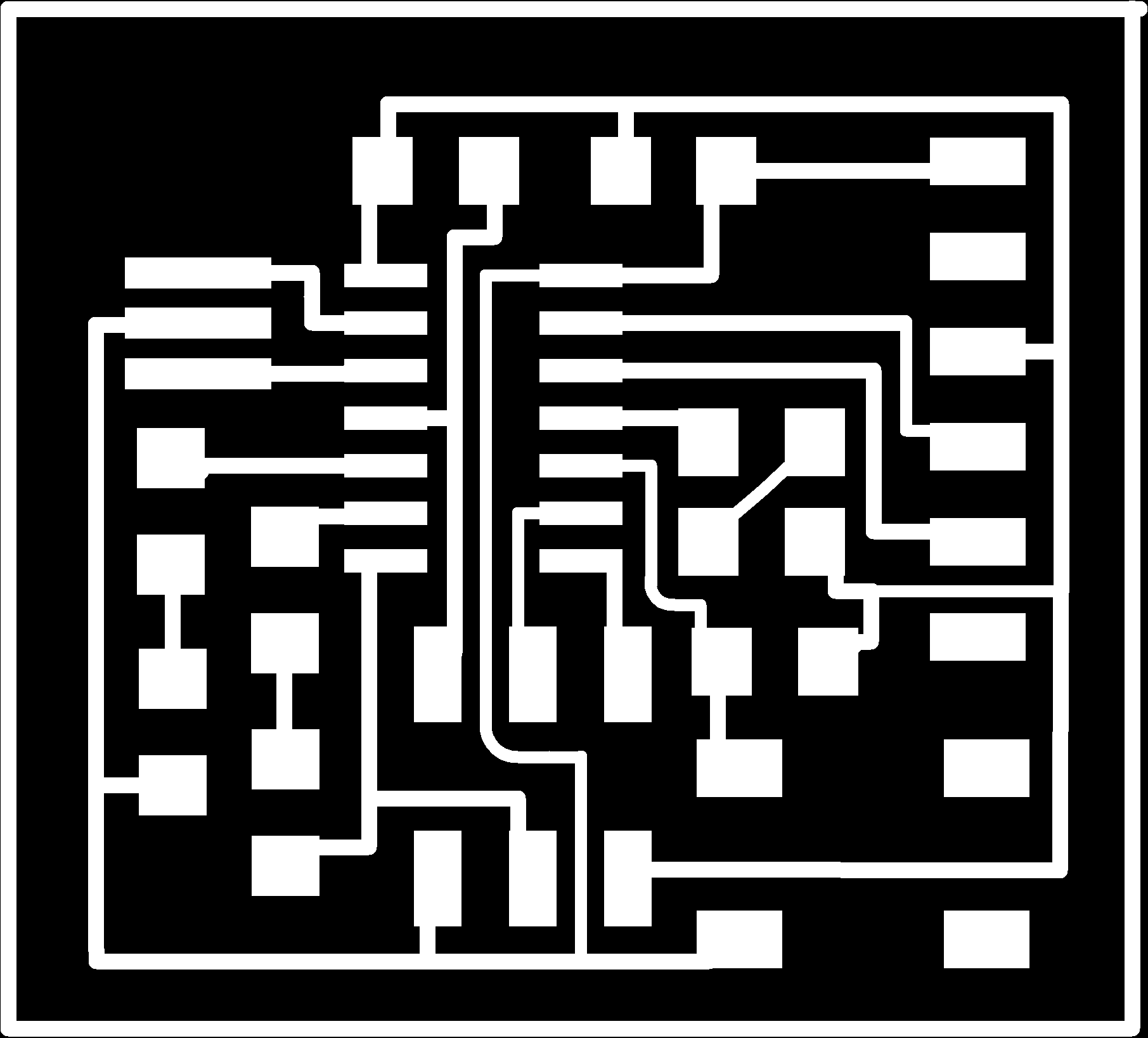
..soon changed it to draw other routes.
Note: Work on layout and schematic, almost simultaneously. Otherwise, it will be hard to draw routes.
Redrawing+adding LED&button
1. I had difficulty understanding this circuit, and drawing it with my hand was really helpful.
2. I included LED and button, and soon realized that the FTDI connector is located too far from the rectangular boundary.
I thought of making different boundary, but maybe next time. This time, practicing with Eagle is more important, so I decided to draw it all over again.
3. From Edu, I learned that LED (with Res) is connected to one pin of MCU, and the other side to VCC/GND or any other pin.
And it looked spacious even with 1 led and button.
So I decided to include more LEDs with different settings just to see what happens. I added 3 LEDs.
4. Hard part was done.
5. Included all, and then 'drc(design rule check)'!
LED1 with VCC, LED2 with MOSI (which is just any arbitrary pin), and LED3 with GND.
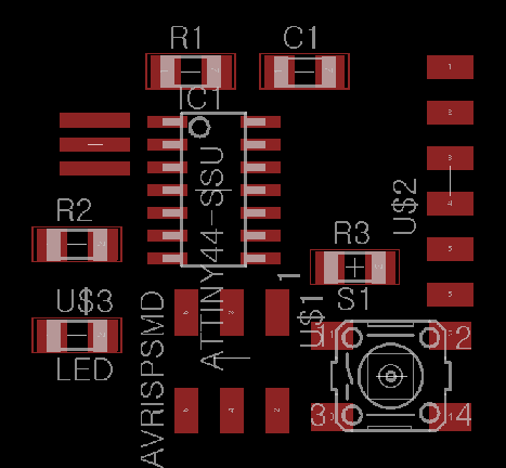
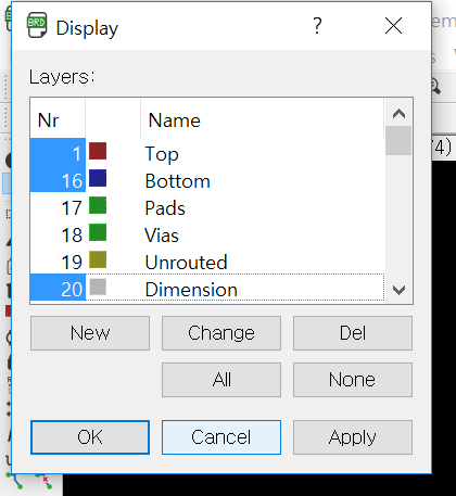
6. Click layer settings, and deselect everything except: 1.Top, 2.Bottom, 20.Dimension, and then apply.
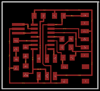
7. Dimension can be used for the outline, so erase (trash bin) the big boundary, and redraw it around the circuit. I used thick line so that I can easily handle it later.
8. File>export>image: check 'Monochrome', file: some png file, Resolution:500~1500dpi, area:full
9. Open it in any 2D graphic application, and fill the thick boundary with black.
But the problem occurred!!
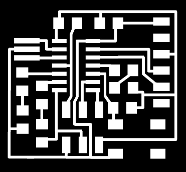
When I used this file in fabmodules.org, in the several spots, the calculated trace failed to distinguish two distinct regions.
The solution that worked greatly was to change route width:0.016==>0.012 and redraw the routes for some parts.
Using some circular routes, and shifting the components were also helpful.
Now it is okay!
10. As for the outline, I used 'drawing rectangle tool' in Paint or Gimp to draw a little smaller rectangle than the boundary (but big enough to cover the circuit part), and then cut it off.
(Download files here: Trace, Outline, and Eagle file. For the outline, you need to adjust the dpi(~962) so that the dimension of the board is the same as the trace board.)
It is not easy to include all the routes properly. My tip is:
- VCC/GND connections are shown most frequently. Try to connect other things first.
- Don't connect too many in schematic page in one time.
- normal route width=0.016, but use 0.012 when needed.
- If needed, use smaller grid.
Misc
- VCC, GND of ATtiny 44 : already detected even before naming and labelling.
- pin 2 of 6pin ISP=VCC, circle of ATtiny 44=VCC
- On schematic page: 'erc', layout page: 'drc'
- 'drc': some errors can be ignored as long as they don't cross, or route clearance is wide enough.
- when there is no way out, use 0 Res as a jumper.
- No matter how, it is fine as long as all the VCC (or GND) are connected.
- You can calculate the resistance needed for LED here:LED calculator or using the voltage drop by led (in my case, 1.8V)+5V from USB. Mine should be higher than 80~90Ohm, and I used 499Ohm Res.
trace width calculator - references: echo hello world board, fab academy tutorial - I made 1led,2led,and 3led files separately, but soon realized that I can just get rid of the copper connection if I don't want some of them.
Making PCB
1. Mill it!
Now the board is ready.
2. Soldering.. is just soldering. Nothing new. The only thing to remember is:
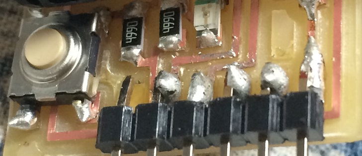
- Additional parts: three LEDs (of the same color. I want to compare the brightness.), four 499Ohm Resistors, 1 button(6MM Omron switch)
- Soldering FTDI was a bit hard at first, but I soon realized that it would be easier to put some solder on all pads first, put FTDI pins on them, apply more solder on it, and then connect the solder on the above and the below. So I desoldered FTDI first, but damaged the copper layer for one pin. Fortunately, it was not connected to any pin, so I could still use it. This new way is much easier. Update: I heard that it's better to have pins connected to the copper layer directly, not through the solder. So I desolder it again, and solder it in a biased way.
Testing PCB
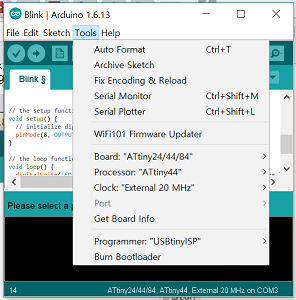
1. download arduino 1.6.13
2. I followed the direction given in Highlowtech such as adding attiny to arduino IDE('File> preferance':add URL, 'Tool> Board'-> attiny:install, etc.) plus clock setting.
3. big short test=smoke test ==> pass!
4. small short test: put FabISP first-->device manager shows USBtinyISP-->connect my 'echo hello world board'-->check if 'USBtinyISP' disappear-->small short! ==> pass!
5. 'File> Examples> blink' : change pinmode(13,output) to pinmode(8,output)
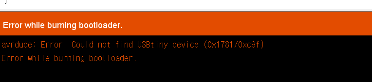
6. 'Tool> Burn Bootloader'
I programmed my USBtinyISP using my Mac, but now I'm using my PC, and didn't have proper environment for programming yet. That's the first problem. I followed the direction in this page to install proper driver. But even after installing it, and even in other computers, it didn't work. It means my echo hello world board must have problems. I have to fix them.
7. So.. I had to stop here, but if it were successful, I was suppose to do the following steps: (Just to remember..)
(1) keeping connected, 'upload using programmer' (with my fabISP)
(2) If everything is working, check FTDI
(3) With FTDI: 'Tool> port> upload'
(4) and so on.
I realized that I didn't install drive, so followed the steps in here. Very detailed explanation.
From the lecture:
- Capacitor:block slowly moving signal, pass quickly moving signal
- Inductor: pass slowly moving signal, block quickly moving signal
- LED(light emitting diode) has voltage drop, but not resistance. Don't connect w/o resistor!!
- Transistor: we won't use bipolar one. will use mosfet (N,P type) planted in channel: charge-->change resistance of channel(?and what is Rds?)
- regulator: ex) 30V-->5V. Only before MCU
- amplifier: don't use anymore. MCU has built-in amplifier
- Applications: 123D Circuits Virtual Breadboard Fritzing is very elementary level/ Eagle is more proper for us (fab.lbr:library)/ KiCad seems good, but not integrated/ Tanner, etc:integrated circuit
- Fusion360, solidworks PCB: physical design+elec design.
- Spice, Gnucap, Qucs, etc.: simulation. For complex circuit, simulate before fabrication!
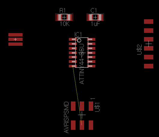
 At first, I connected like this, but...
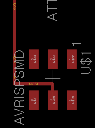 ..soon changed it to draw other routes.
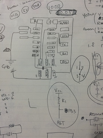
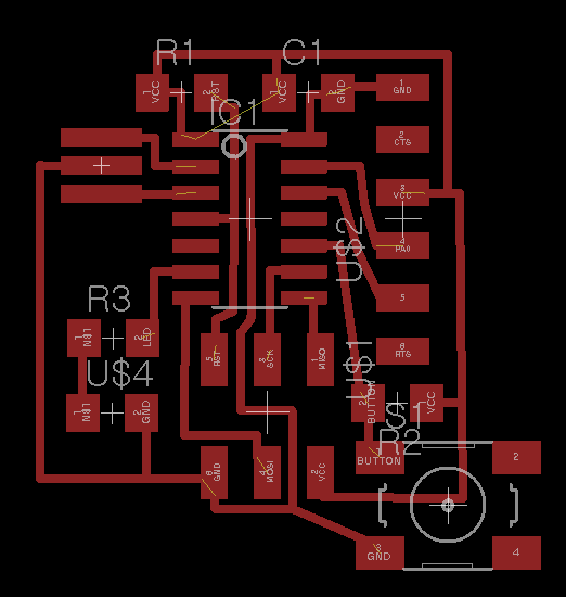
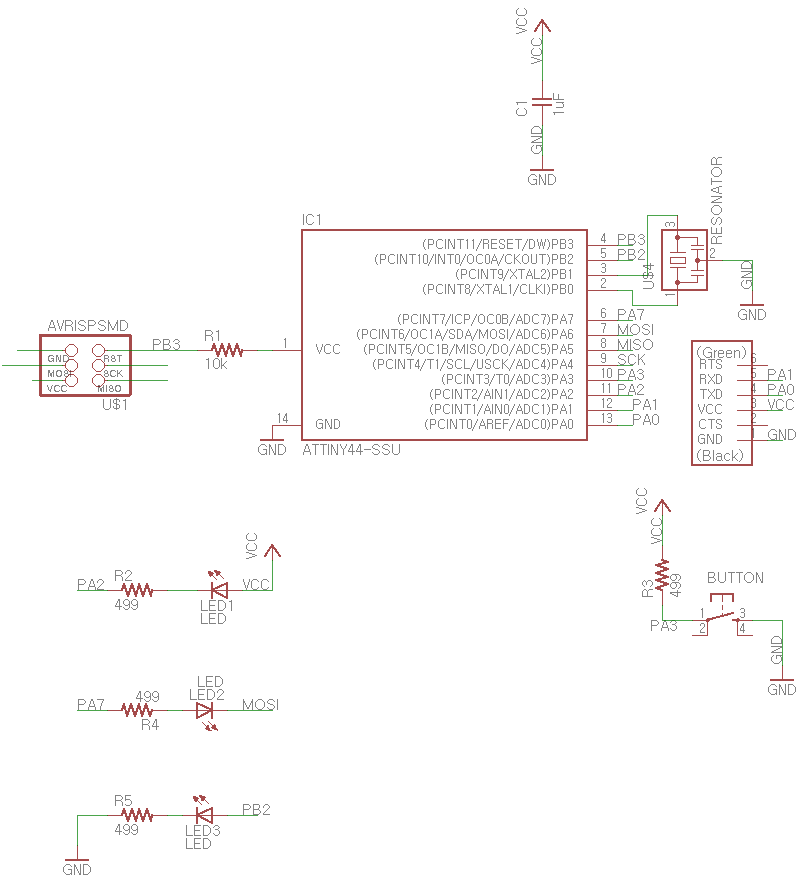
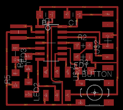 LED1 with VCC, LED2 with MOSI (which is just any arbitrary pin), and LED3 with GND.


