Assignment 06
Electronics Design
Assignment:
Redraw the echo hello-world board and add at least a button and LED with current limiting resistor or design your own.
Learning outcomes:
- Select and use software for circuit board design
- Demonstrate workflows used in circuit design
Have you:
- [x] Shown your process using words/images/screenshots
- [x] Explained problems and how you fixed them
- [x] Done fabbercise today
- [x] Included original design files
This week's recitation
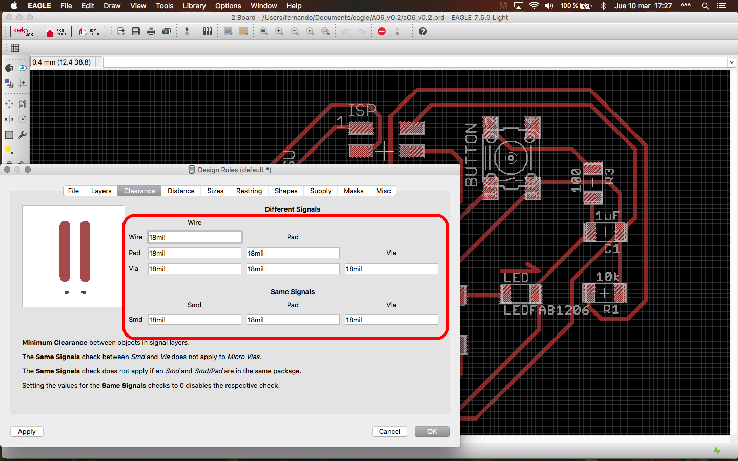
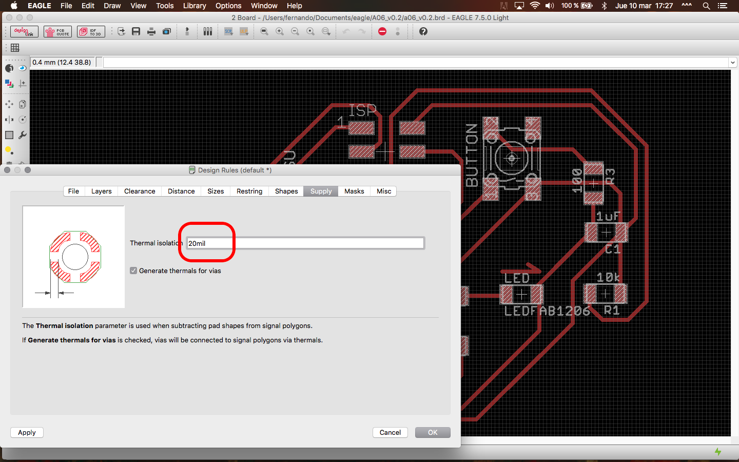
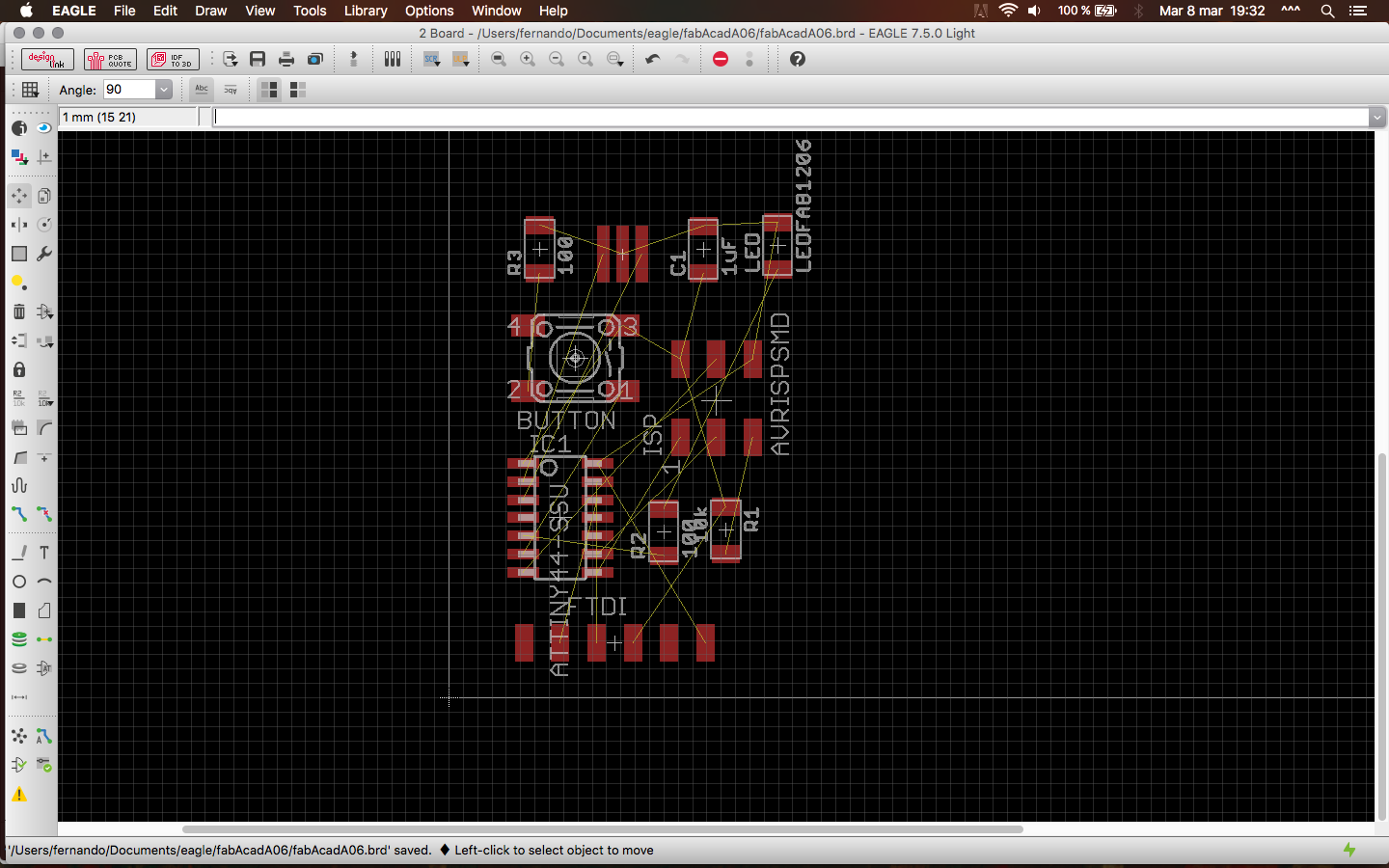
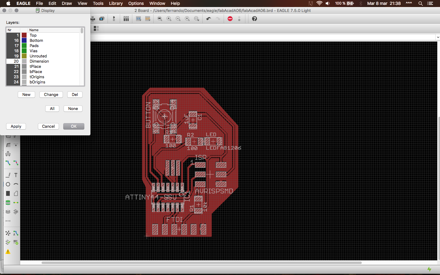
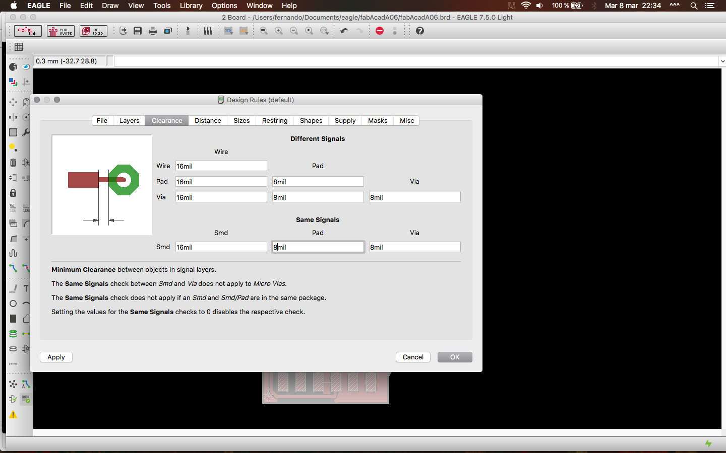
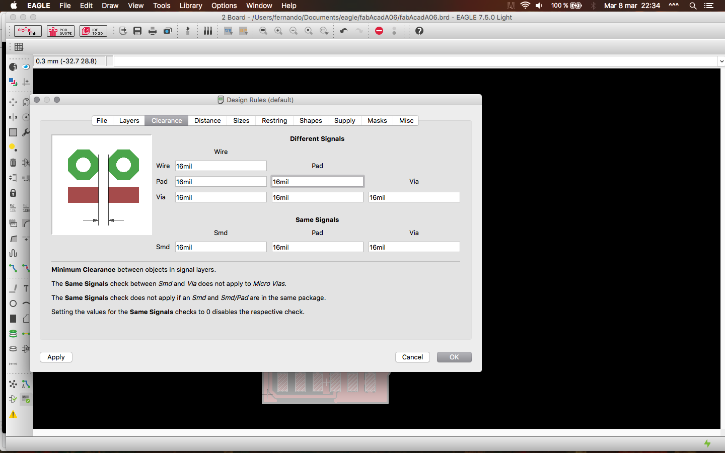
So, after the first experience, I first edited the Eagle's design rules and then started to re-route everything ... note that the modified values belong to the "Clearance" and "Supply" tabs. The last modifies the bridges sizes (see previous entry).
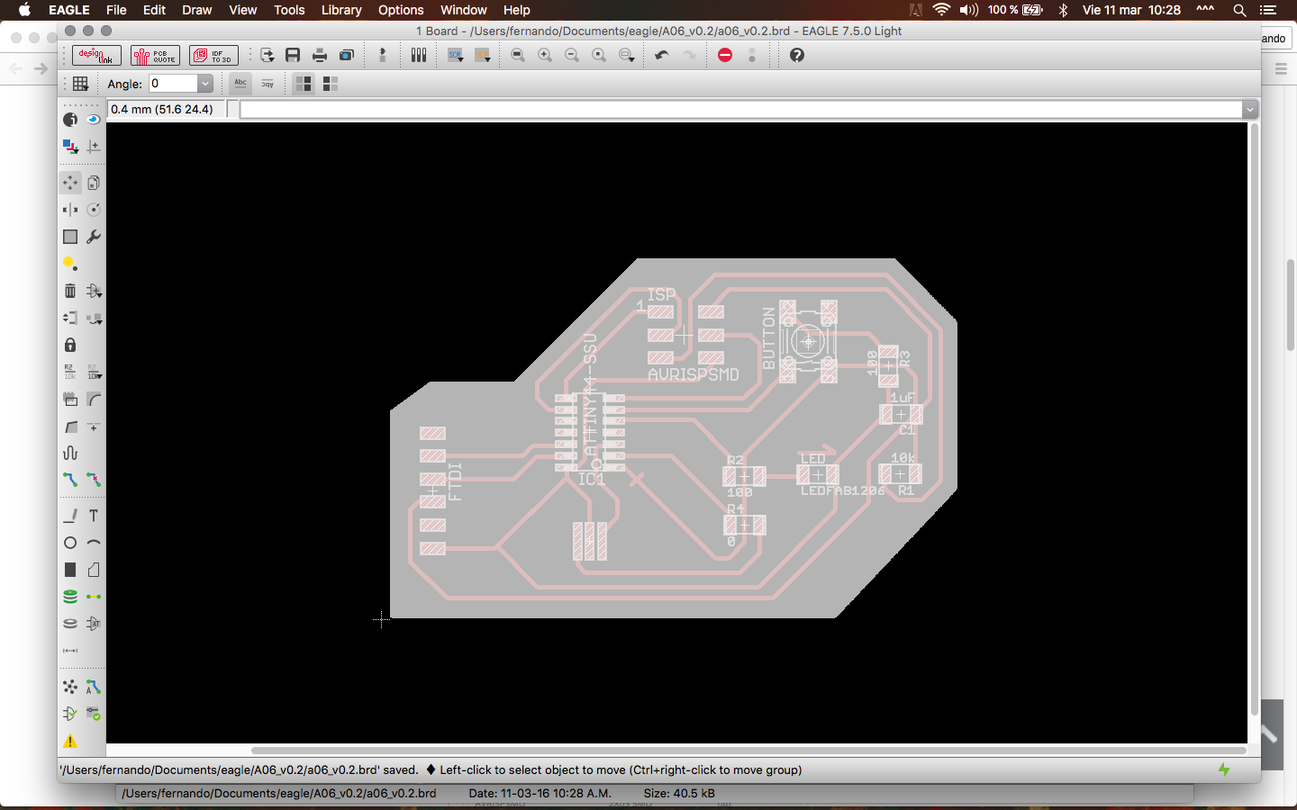
For my suprise, in this attemp I had to use a 0 Ohm resistance to connect the routes (my classmates didn't need to, and I know it can be done without it), since after many restarts I always had the split ground issue (components with disconnected grounds).
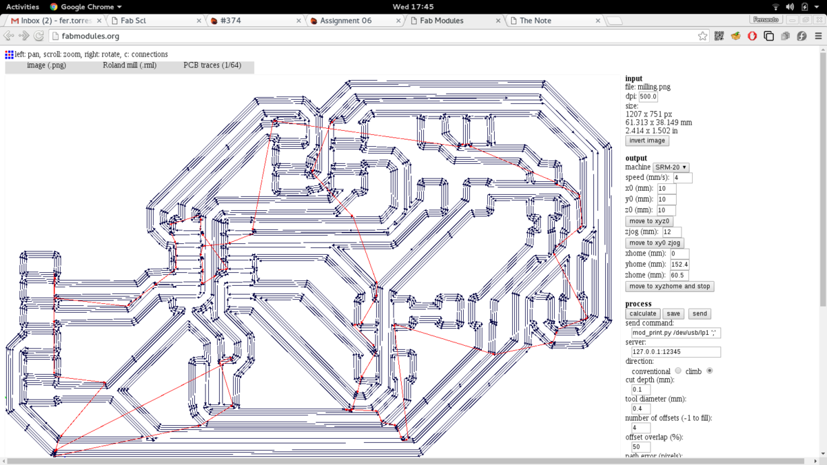
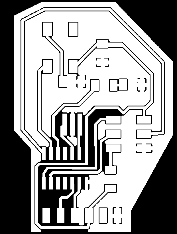
But who cares ... the milling images worked fine for the traces ... but when I made the outside cutting I realized that the polygon I made was too close to the layout, so when I made the milling it ate a part of the board (I made the VCC trace rounding the PBC's edge ... not recommended ...)
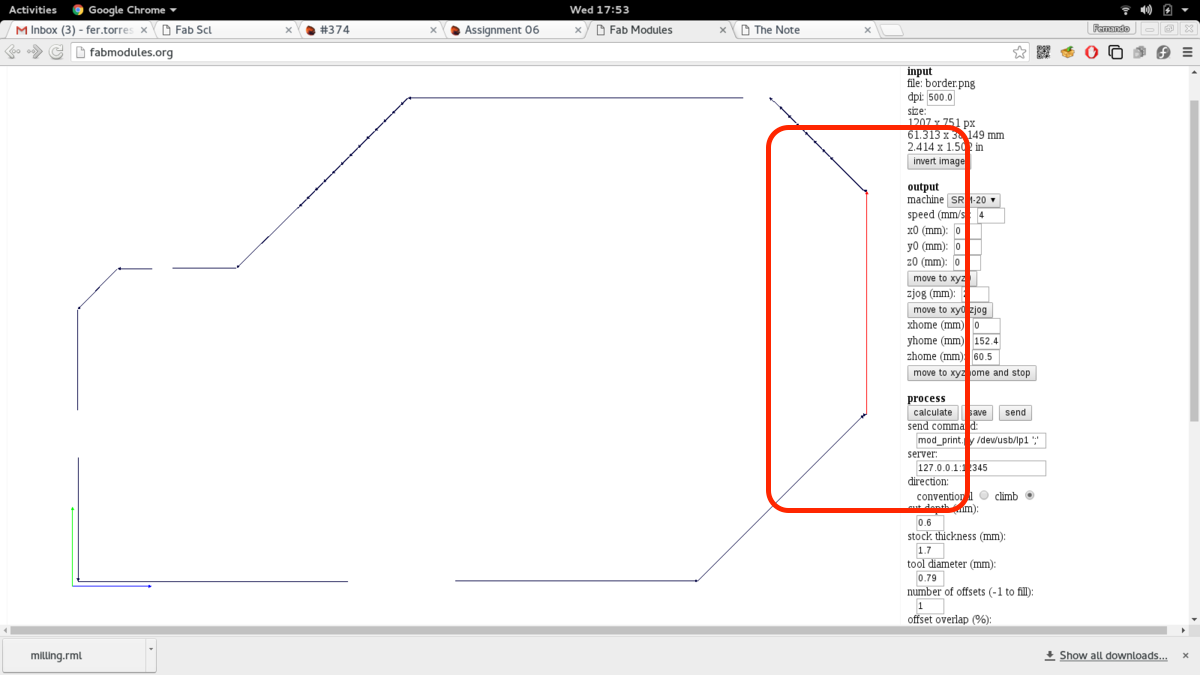
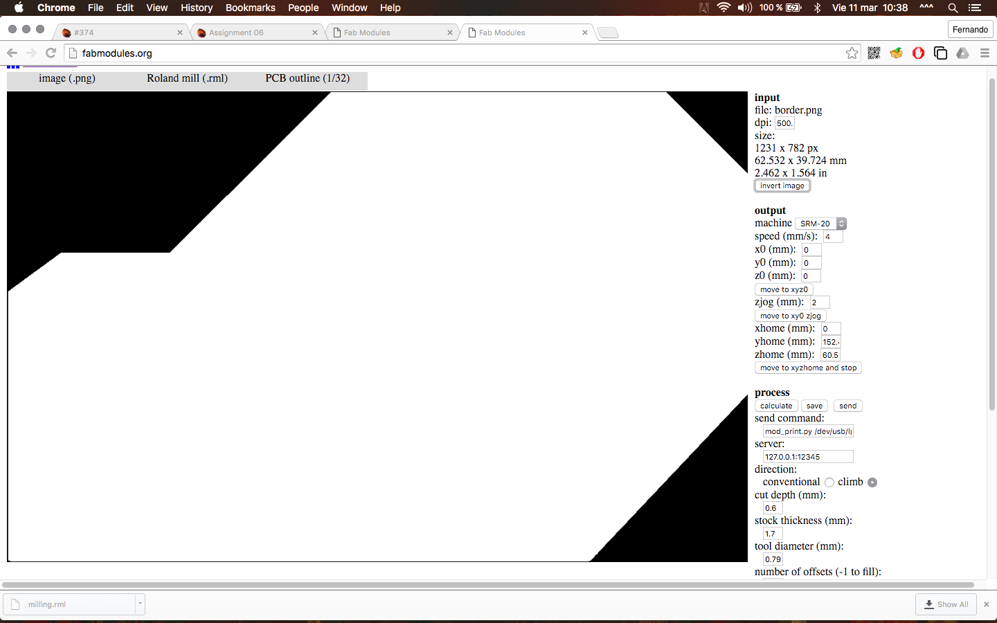
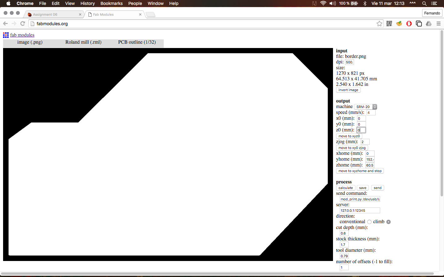
And, in fact, there was and edge that wasn't cut at all! (see images), and then I realized that the meaning of the red line in the right most side of the fabmodules images for the border cut out (not going to be done ...). My suspicion is that the border image need a frame ... the edge I want to mill is too close the the image's border.
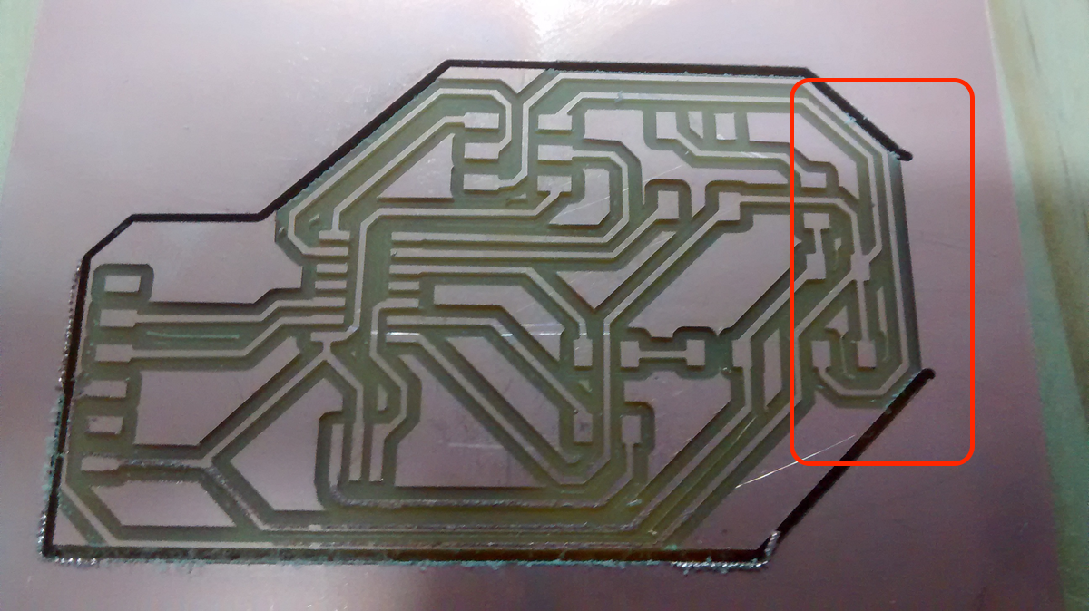
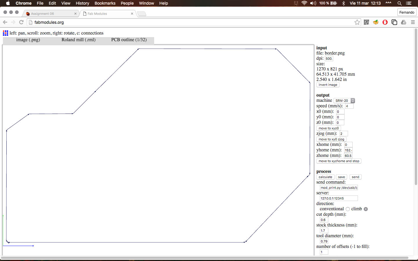
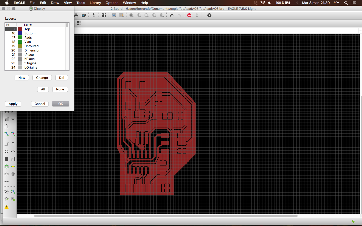
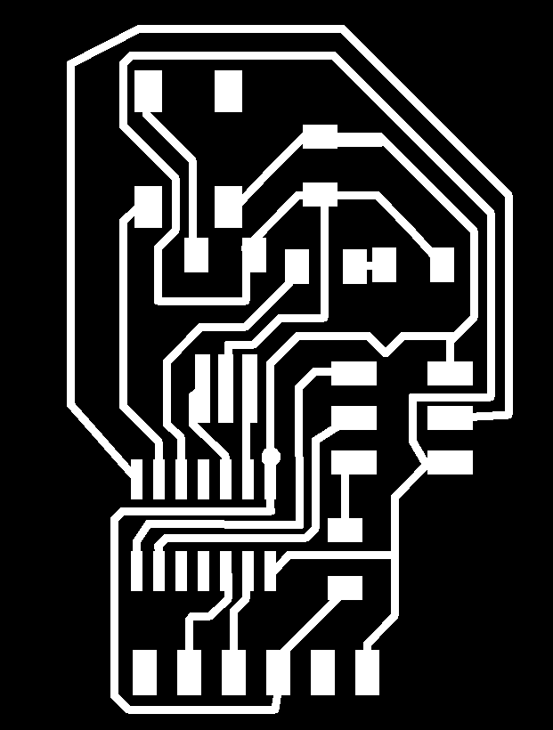
So, at this point I need to redraw a bigger Dimension layer to cut out the board without affecting the main board. Through inspection of the previously cutted board, I saw that one of the borders actually went well, so I checked it on the Eagle file and verify that it has something about 2mm distance from the traces, so I replicated that distance all around the PCB edges.
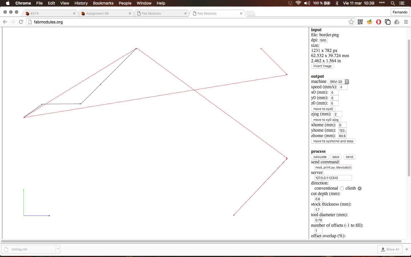
First I tried with the image as it comes out form Eagle, but it won't take the edges either (images below)
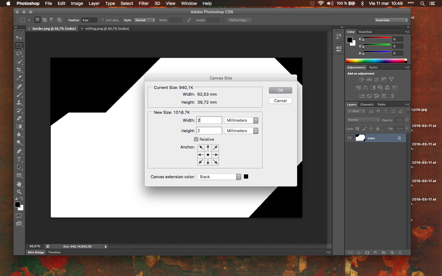
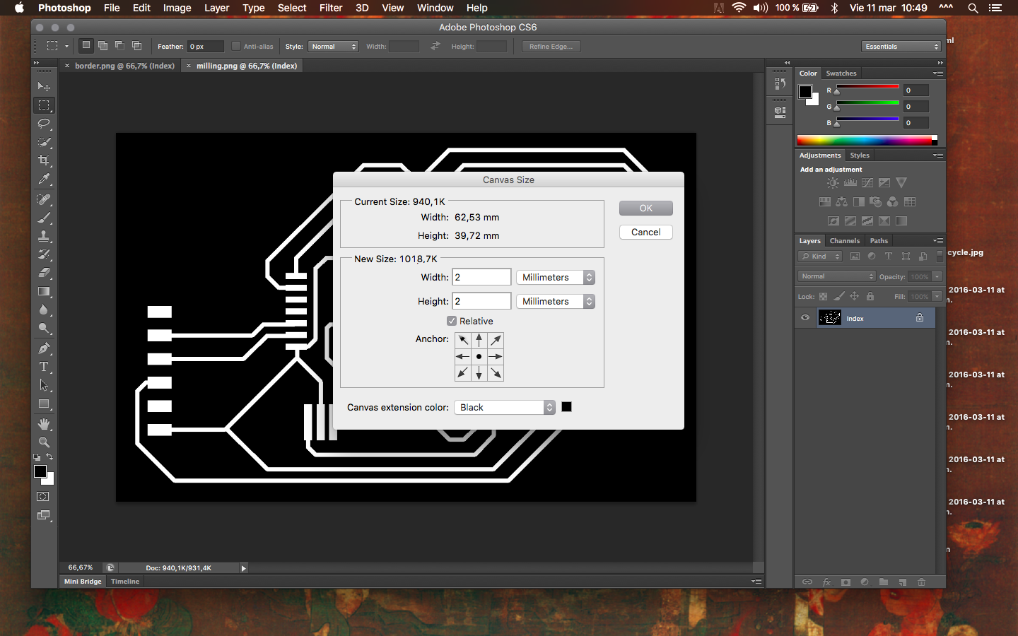
So, I went to Photoshop and simply enlarged the canvas size of both the border and milling traces images by adding 2mm to each side (hope it will enough).
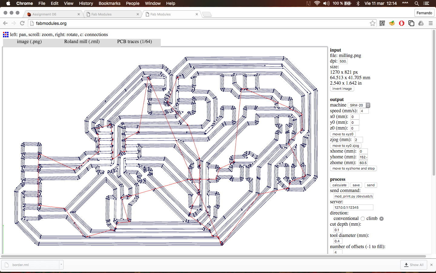
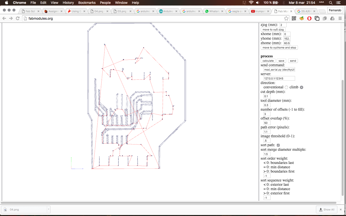
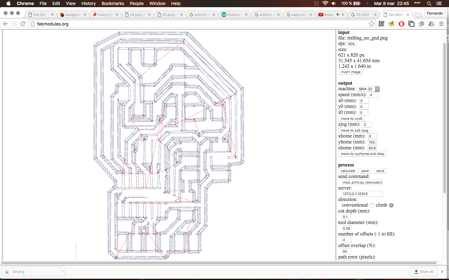
And here are the screenshots of how these modified images worked on fabmodules; and now I feel a little bit optimistic.
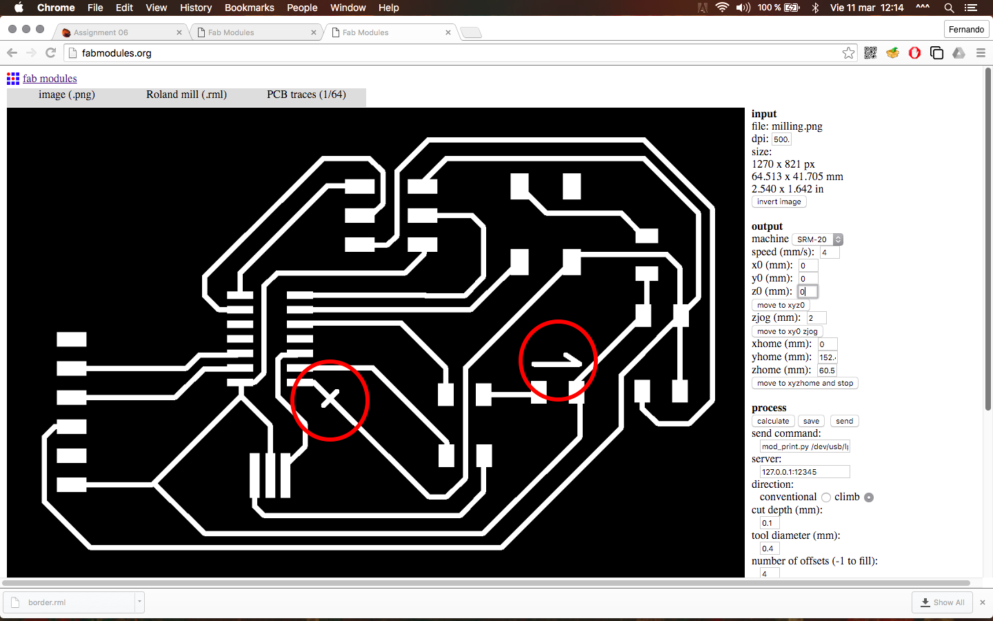
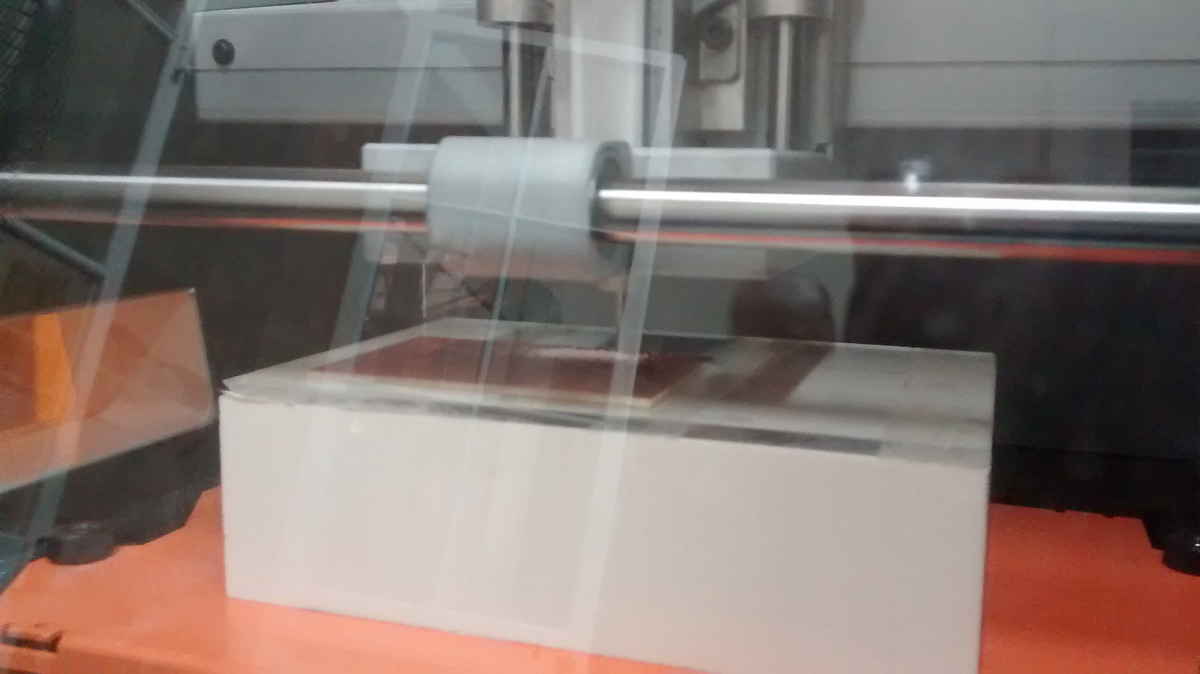
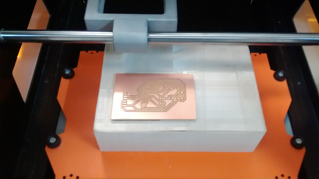
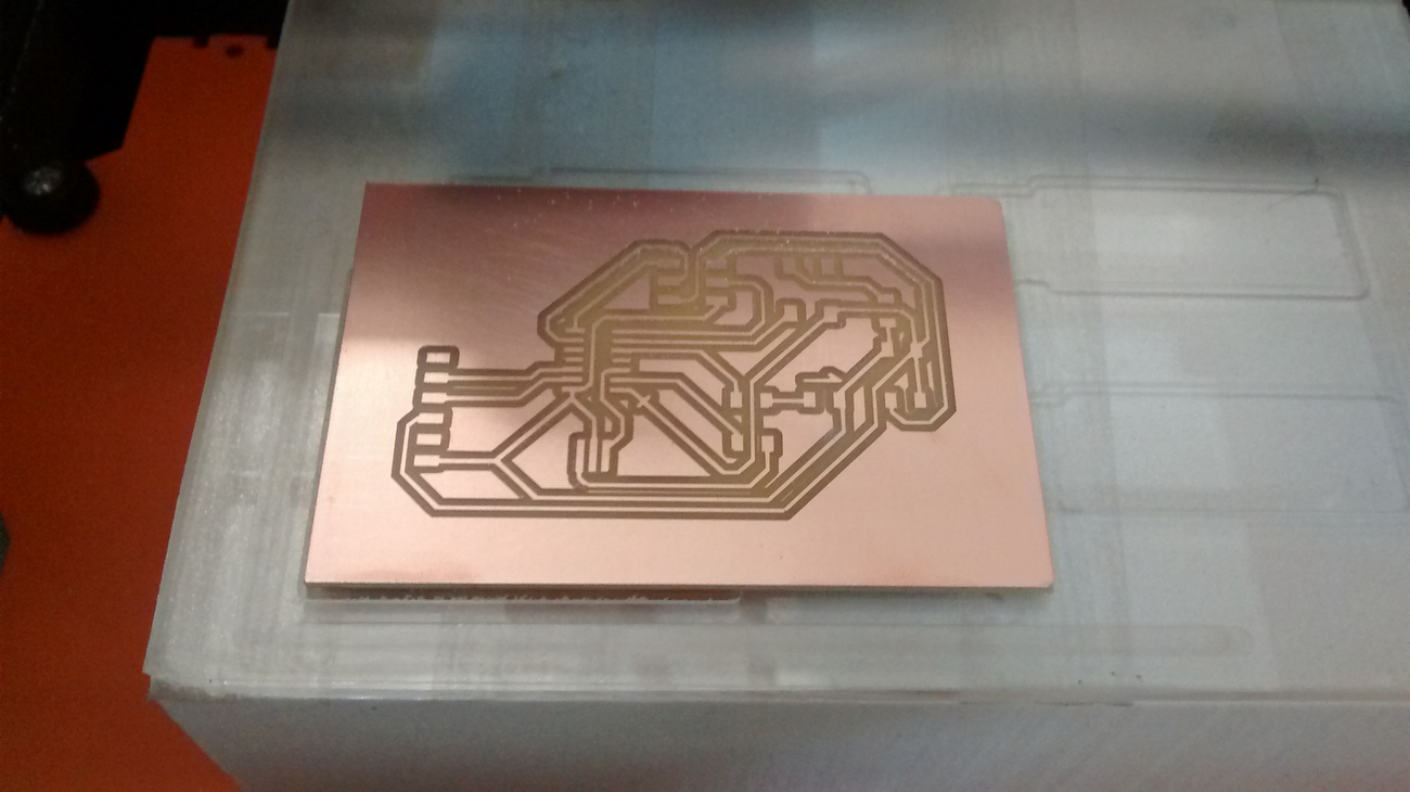
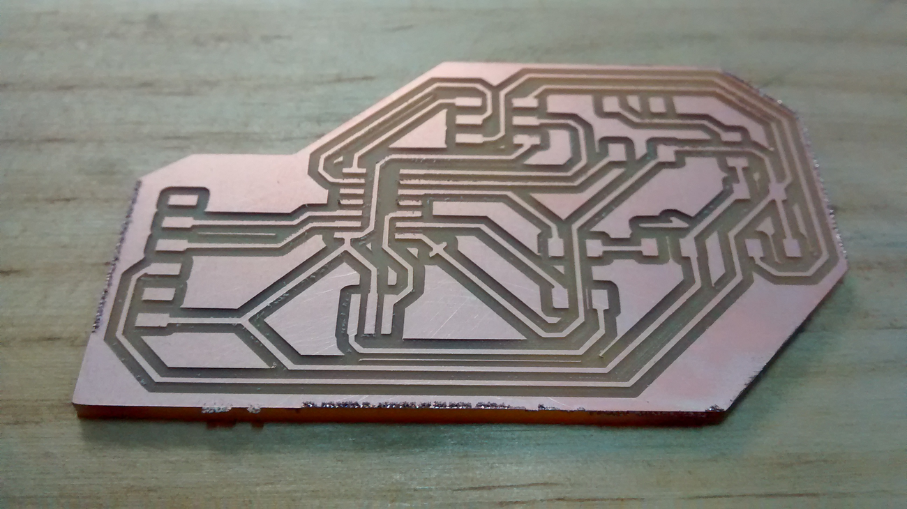
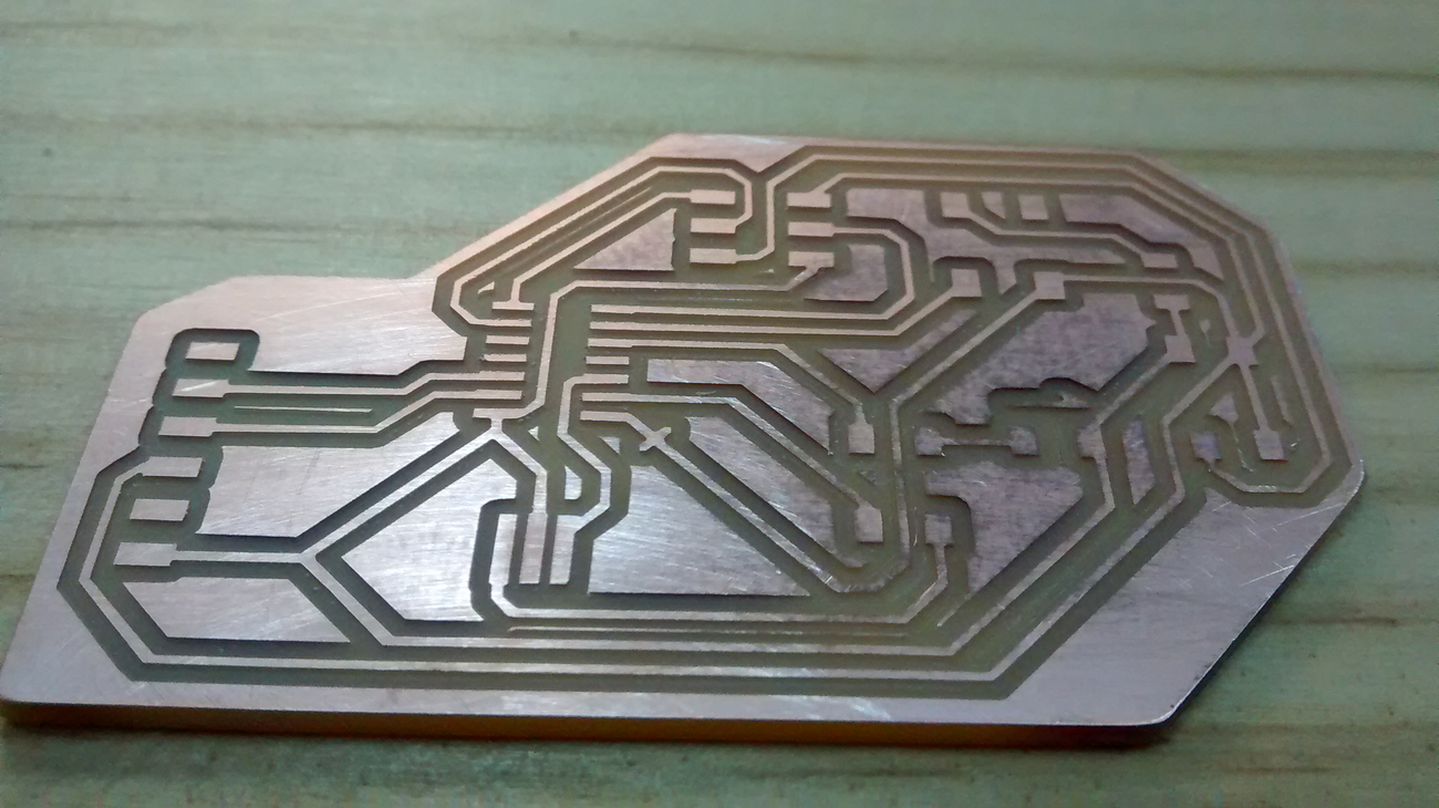
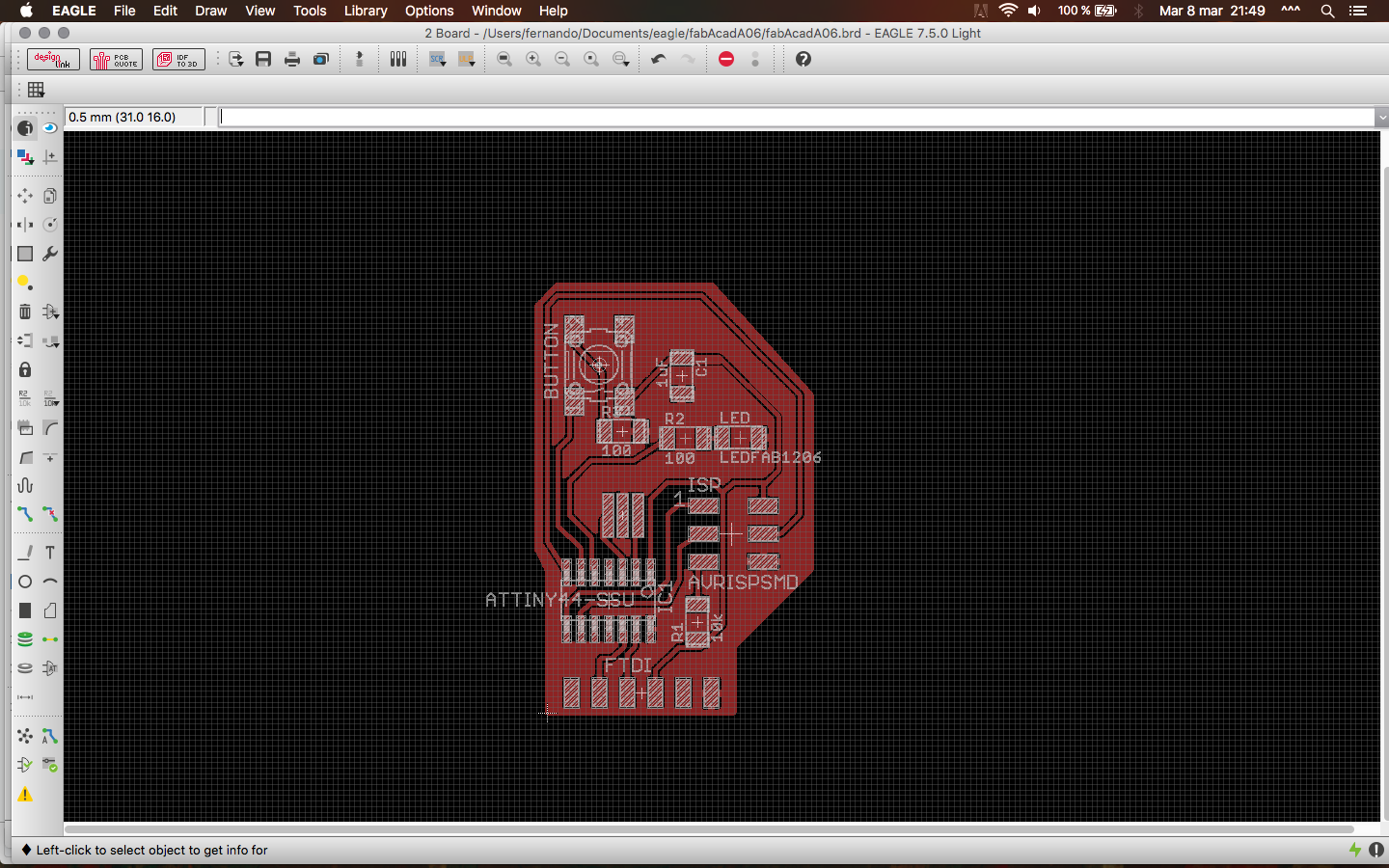
Note the marks I left on the PCB to point the LED direction and the pin_1 of the IC. And now, to mill the PCB again ...
And here are the v0.2 milling results, everything OK ... next step, soldering the components.
Source files:
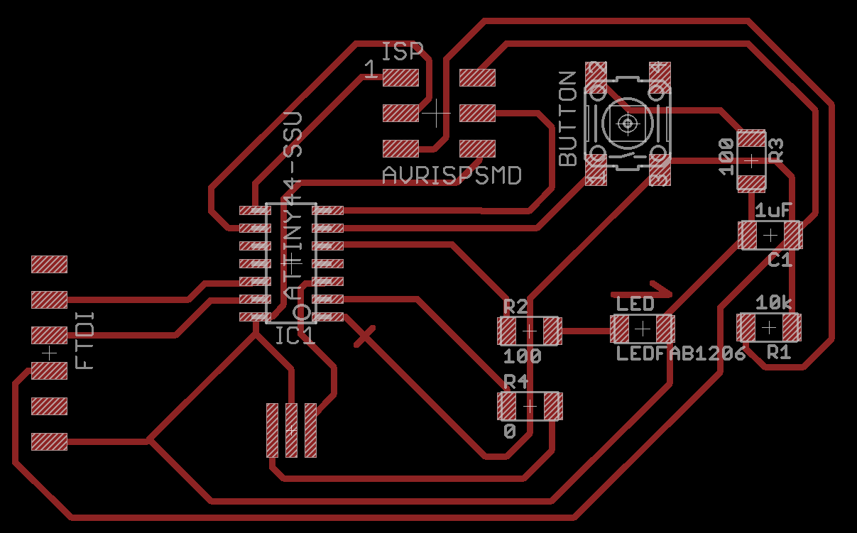
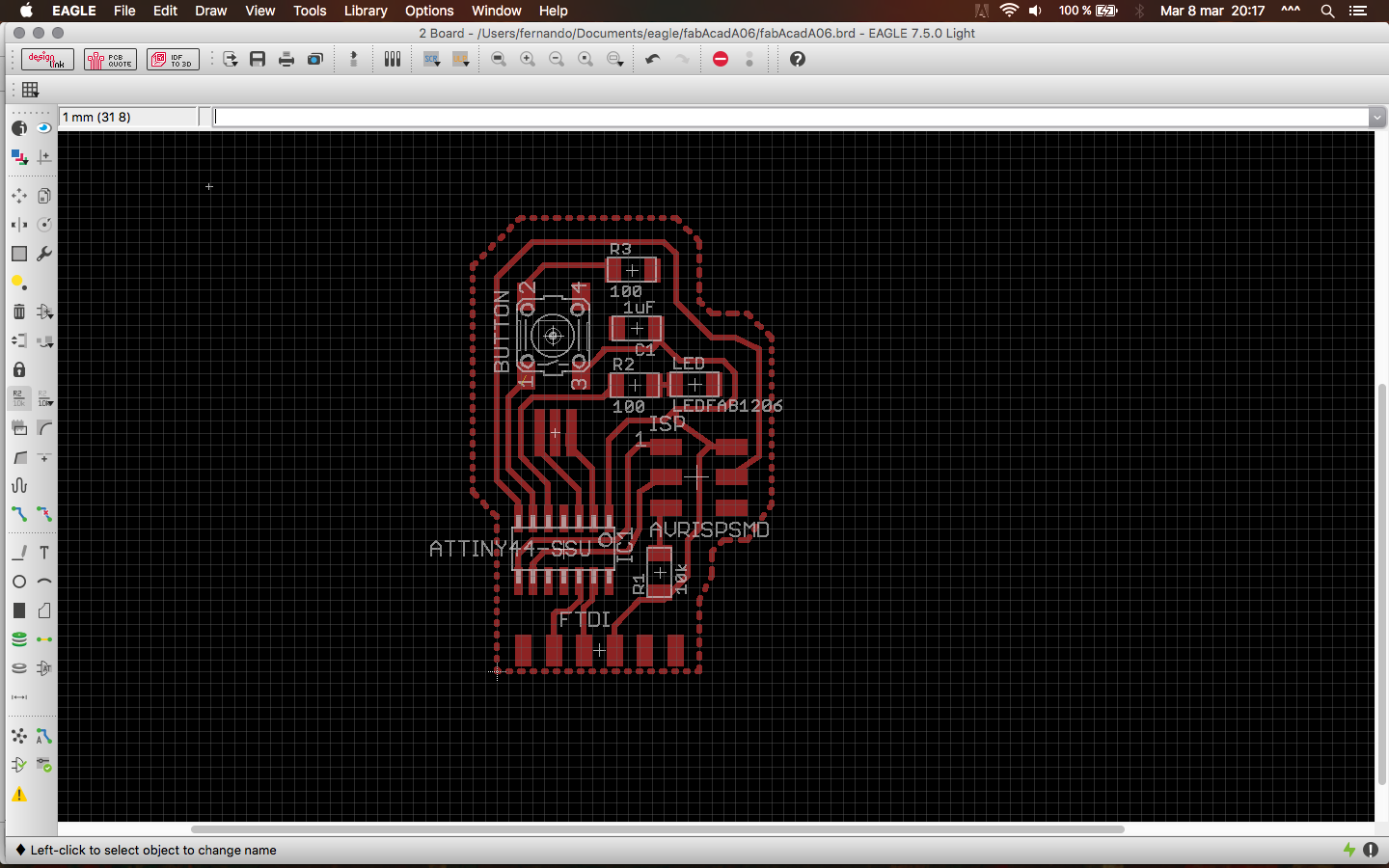
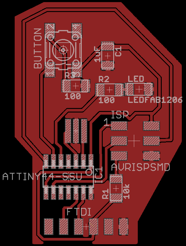
So, this week's home work is to redraw the HelloWorld board and add (at least) a button and a led.
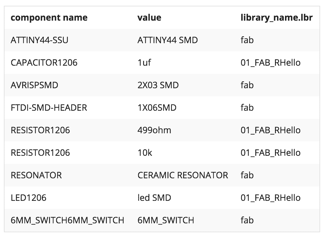
The material list was taken from Giacomo Falaschi site (2015 student, thanks to #371 for the link):
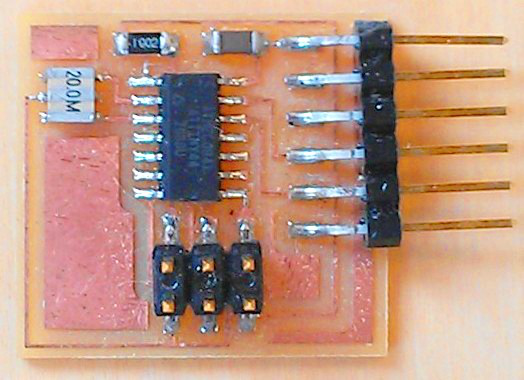
And here are the reference images of the board:
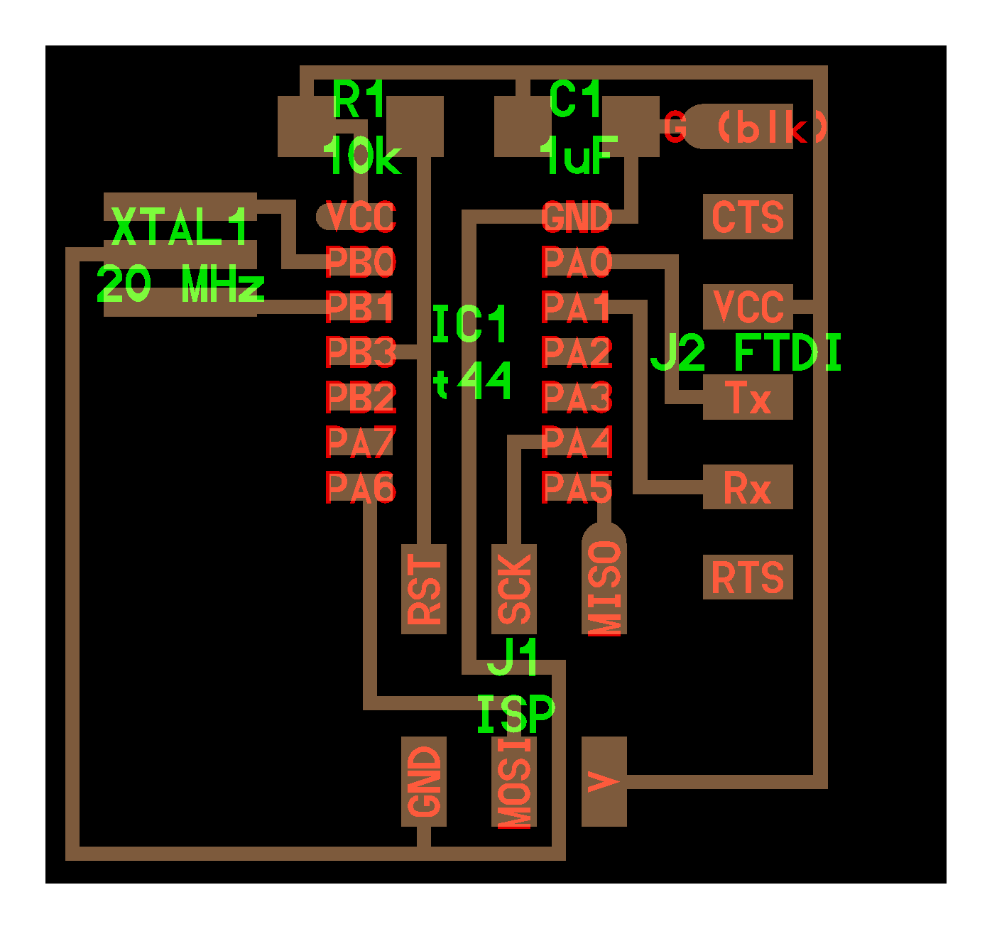
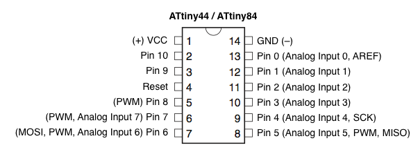
So, one of the issues I'm facing is where can I connect both the button and the led, so I made a quick search on Google to see the correspondance between the Attiny44 and their Arduino pins:
So, what I'll do is to connect the button to VCC and to Pin7 (a.k.a. PA7) so when the button is pressed I'll read the Pin7's state and trigger rise the voltaje on pin8 (a.k.a. PB2), on which I'll connect the LED. And, to avoid noisy signals, I'll use the pulldown circuit shown in the Arduino Button example.
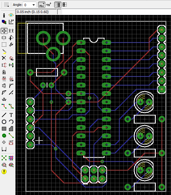
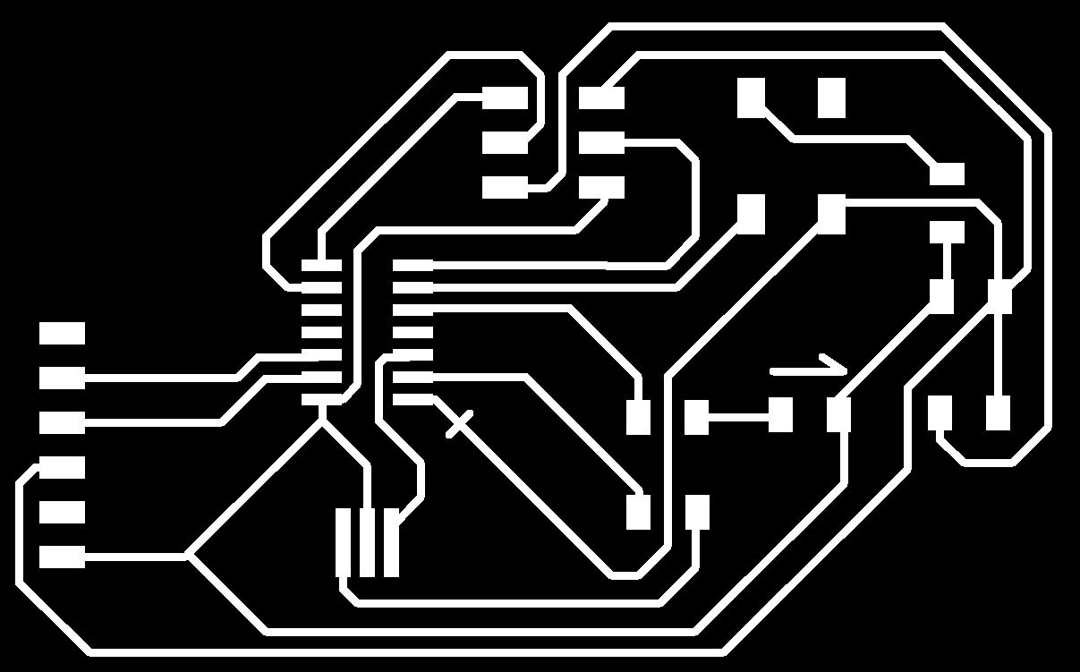
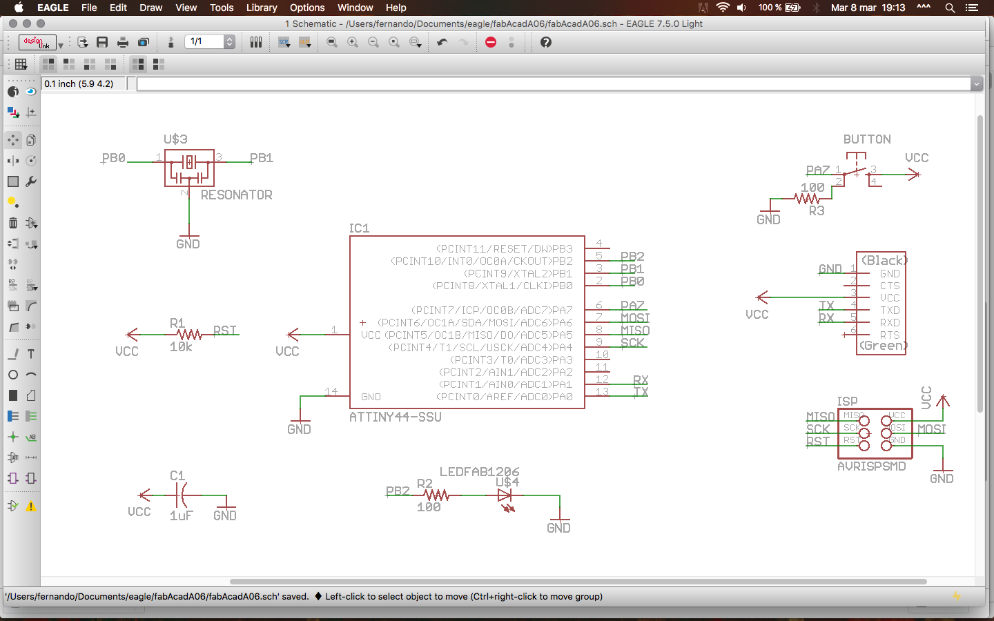
After finishing the schematics I started drawing the PCB routes, which took me quite a while, until all the routes where complete. Then I made the DRC (Design Rule Check) and everything OK. SPOILER ALERT: this design didn't make it ...
As posted in the previous entry, I went for the trick of setting the top layer as GND, which generates some small bridges between the components ground connection and the layer, but these bridges tuned out to be too thin to be milled, as shown in the fabmodules image (below).
Thus, I went to the design rules to make those bridges thicker and to get the design suitable for the milling machine, BUT at the moment of re-doing thr DRC the armageddon appeared ... lots of error messages!
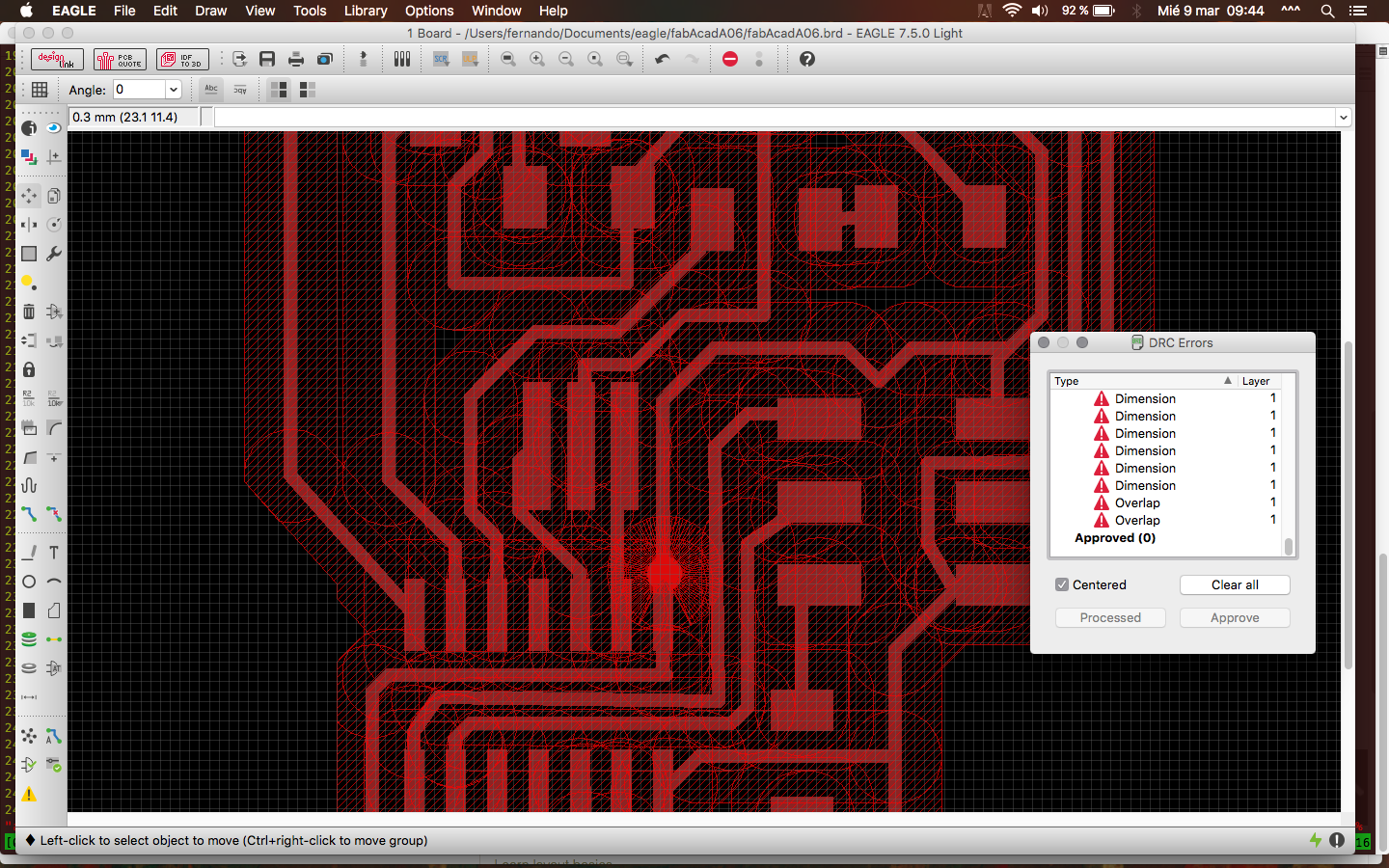
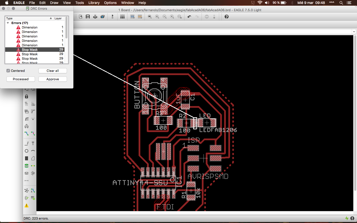
I tried re-adjusting everything for a long while (~3hrs), tried undoing the GND top layer trick, etc ... but I confess that at some point I just said no more ... and started from the board routing again from scratch.
NOTE: Just to make a record of it, I got fabmodules to generate the paths for this version of the PCB, but as I had too many unhandled errors on the sources file, I decided to discard this deceptive version.
So, first things first ... to the Eagle tutorial on Sparkfun
In short, we need to:
- Install and setup (install useful parts libraries): In short, add the folder containg the new libraries (.lbr files) to the Libraries path under "Options -> Directories"
- Learn schematics basics
- Learn layout basics
Here are the tutorial files (.brd not finished yet): file 1 file 2. And here is the fab.lbr.
NOTE: One of the remarkable tips provided in the layout tutorial is to set the top layer as GND, which help minimizing the surface to mill and to help connecting the components in an efficient way (source link):