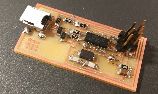
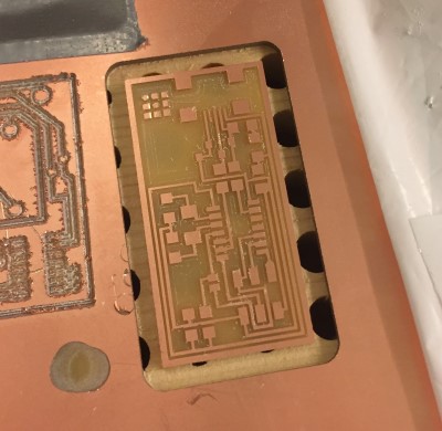
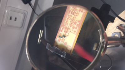
Here is my finished board.
My tutorial for using the FabISP to program the Hello Echo board
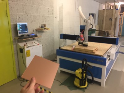
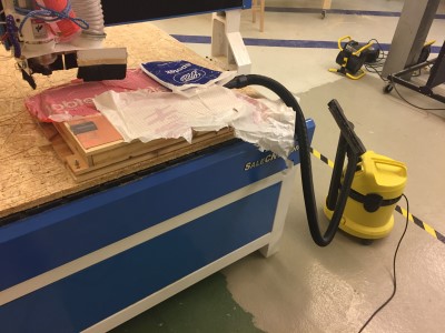
Verket Fab lab where I am taking the fab academy is equipped with a SaleCNC.com CNC router and a windows laptop running the Mach3 CNC control software. It has recently been equipped with a home made vaccum-cleaner powered vaccum table which we will use to mount our FR1 circuit board stock to.
During week2 we had a visit in the lab from our local instructor Jens Dyvik from Fellesverkstedet Fab Lab in Oslo. He helped us test-mill the PCB for the hello.ISP.44 version of the FabISP to verify that the machine was capable enought to do it. I now used the file from that experiment as a starting point for learning RhinoCam which is a milling path generator for the 3D modeling program Rhinoceros.
I choose to also use the hello.ISP.44 layout from the 2017 class archive for my FabISP to be able to improve on the previous milling experiment.
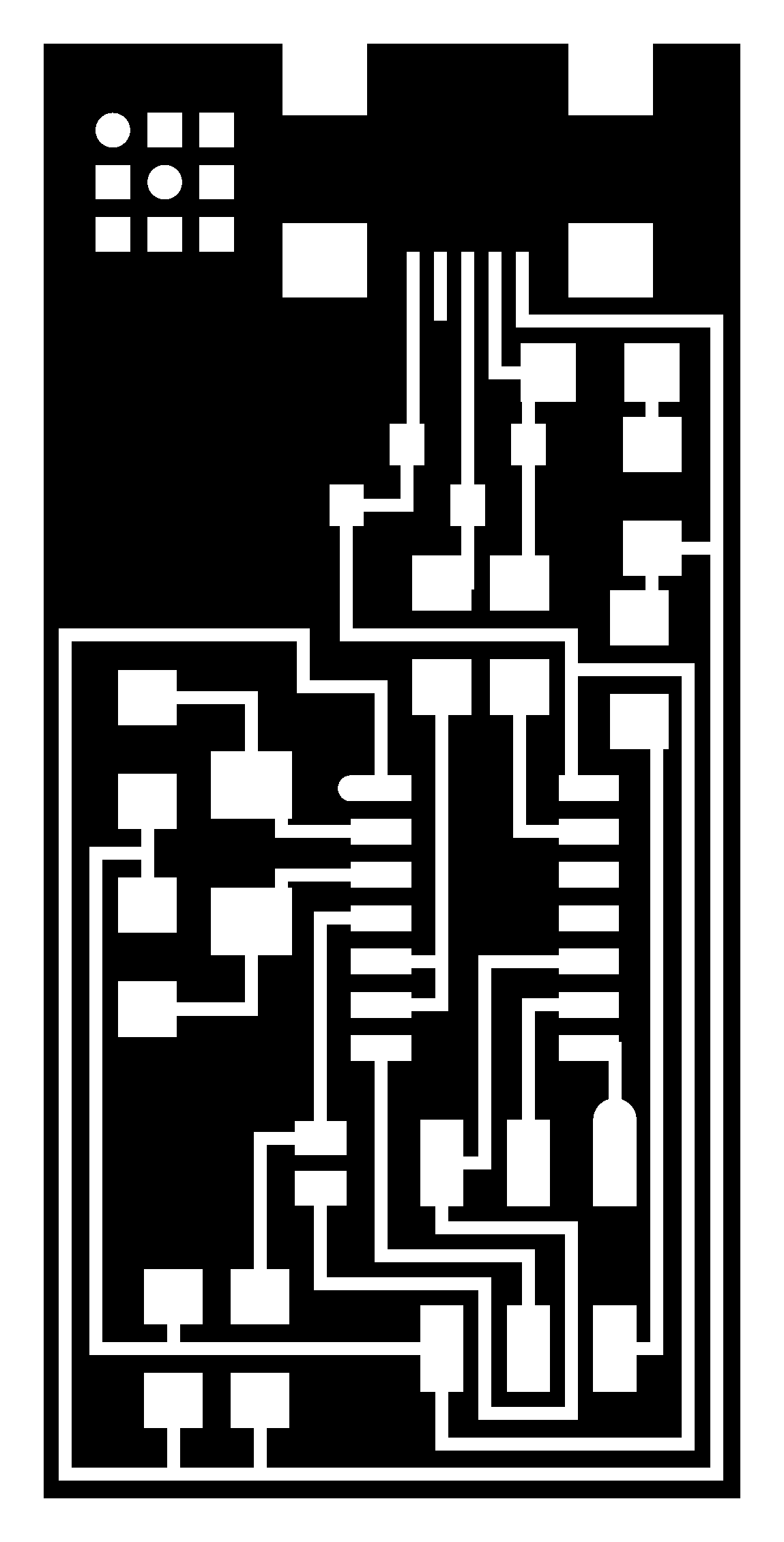
I imported the hello.isp.44.traces.png (show below, right click to save) into Inscape and used the trace bitmap command to generate a vector image which I exported as hello.isp.44.traces.pdf for import into RhinoCam.
Below you see both the milling paths in RhinoCAM and the milled card from the previous experiment.
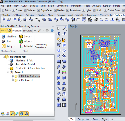
The amount of settings for even such a basic job is quite daunting and I will not cover all of them here. Here are the basic settings used in the program during the experiment. I used them as my starting point.
The lab already had a post processor calibrated so that RhinoCAM could generate the correct g-code that Mach3 will use to control the machine. Anyway I double checked that the start and end of the code looked the same as a reference file on the Mach3 laptop before running the file.
To mill the circuit I placed a piece of FR1 PCB stock on the vaccum table and sealed the rest of the table with plasic bags to ensure a good vaccum on the board. During the milling I kept tesing the the vaccum-cleaner exhaust air temperature with my hand to make sure that it didn't overheat from the reduced airflow.
I inserted the correct milling bit and manually drove the tip to the center of where I wanted to mill the card. I then placed a paper on the stock and carefully tapped the Z-down button until the bit hit the top of the paper. I then overrode the X, Y values manually in the Mach3 interface so that I saw that the preview was aligned with the center of the card at X40 and Y50. I then set the current Z height to be Z0.1mm to compensate for the paper I used. Next time I'll try the trick of adjusting the Z by sliding the milling bit out of the collet instead, but I think it might be more tricky with this big collet.
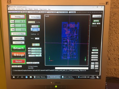
I started the milling program and saw that I was too high in Z.
So I adjusted Z again by stopping the milling and overriding the Z value in 0.1 mm increments untill the card machined generally fine. However there were some areas that just didn't want to get milled, it didn't seem to matter that I ran over them with several passes, each 0,1 mm deeper than the last one. The problem only appeared in the open areas, never right next to a copper trace.
Finally when I tried a 0.3 mm deep pass I got the mill to clear the stubborn areas.
Then I could run my cut out file to release the milled cricuit board from the stock.
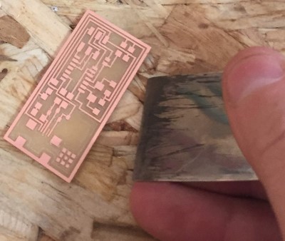
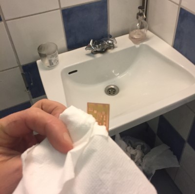
I finished by scraping the card (didn't seem to be much irregularites but it also didn't seem to hurt) and washing it.
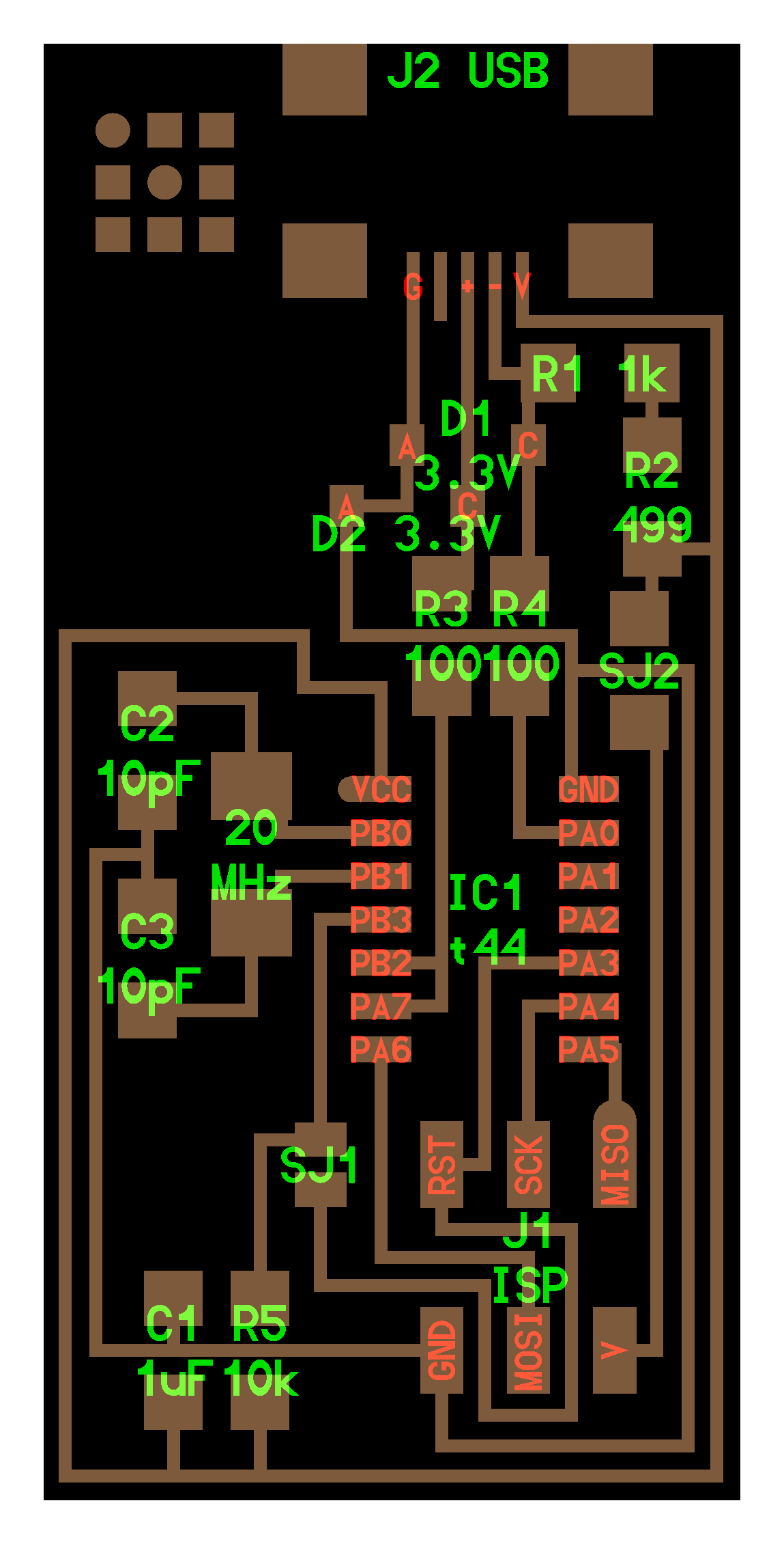
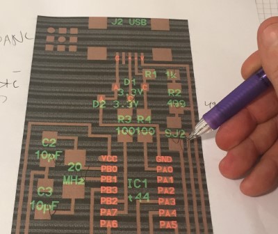
First I located all the component bags needed to "stuff" (add the electronics components to) the board using this image from the lecture notes. It helped knowing that R means resistor, C capacitor, that Mhz indicates an occilator and that diodes have a direction! (Positive Anode Negative Cathode = the PANC rule. The arrow points from + to -, that is from A to C and that means the tiny line on the diode shall be towards the Cathode.)
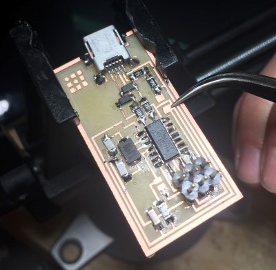
I prepared one or two components at a time to avoid loosing or confusing them. I attached them by first adding some solder to one pad, and then lowering in the component with tweeezers while heating the "puddle" of solder. It was a nice technique!
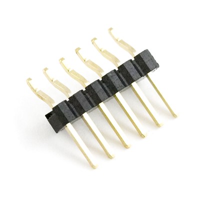
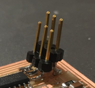
We didn't have any surface mounted 6 pin headers so I made my own by bending two 3-pin pieces of right angle male header strip into shape.
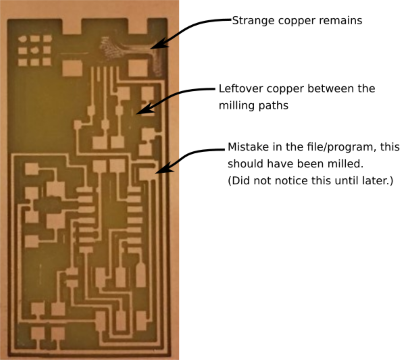
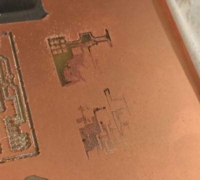
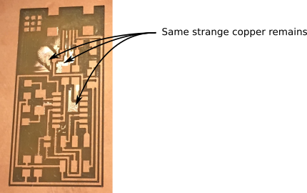
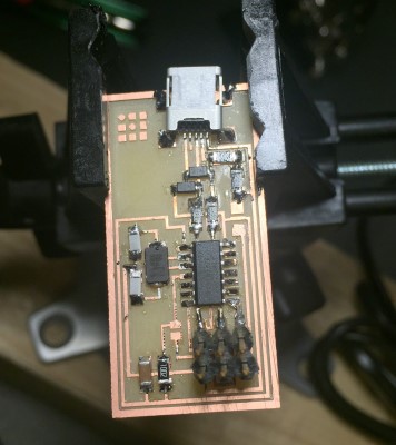
I added componentes and tested them as a went with a multimeter. When I added the header I noticed a short circuit between the VCC header and Ground. It turned out to be a milling error, see pics:
I broke the connection with a knife and remeasured to verify that the short circut was gone.
For the IC and the header I first added to much solder, binding several legs together. But I used a soldering wick to suck up the extra solder and that left a really nice and clean result. That worked so well that I'll consider doing it intentionally the next time around.
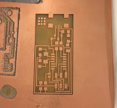
This is the finished board (which I forgot to clean).
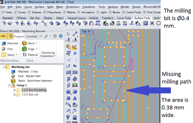
I opened files in RhinoCAD and found why the path wasn't milled correctly.
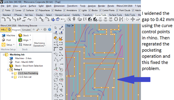
Here is the fixed Mach3 file.
TODO: add rhinocam1 file
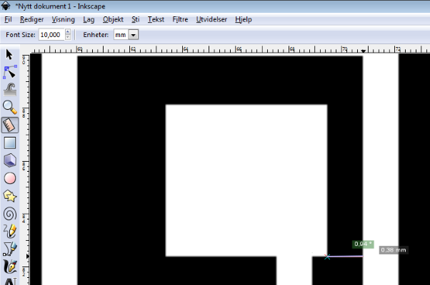
I wanted to know why the file had a too tight gap in the first place so I reopened the original .PNG file in Inkscape and measured the gap. Turns out that it depends on which side of the blurred edge you measure the gap. Inside the start of the blur it is 0.38 mm and outside it is 0.42 mm TODO ADD FIXED HELLO 44 trace
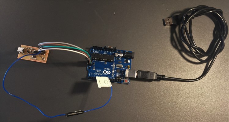
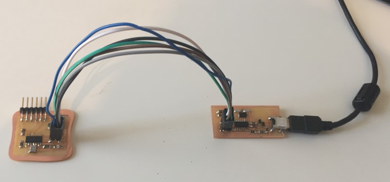
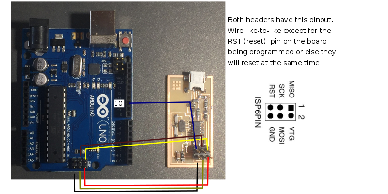
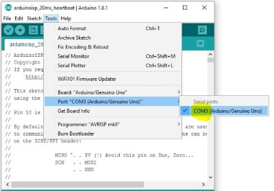
My FabISP version hello.isp.44 being programmed by an Arduino UNO
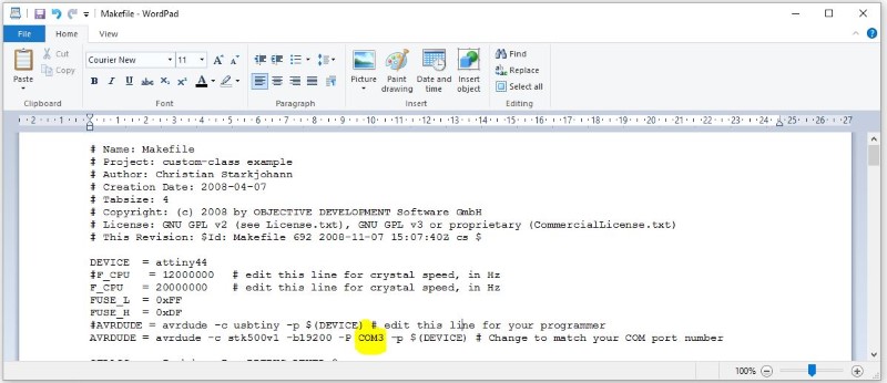
Replace this line
AVRDUDE = avrdude -c avrisp2 -P usb -p $(DEVICE) # edit this line for your programmer
with this line
AVRDUDE = avrdude -c stk500v1 -b19200 -P COM3 -p $(DEVICE)
And edit the COM3 so that it matches the number on your COM port.
Program a hello echo board using your new FabISP
In order to use the FabISP it needs to be programmed. At the time of doing this exercise there was no dedicated In-sytem programmer (ISP) available in the lab. This is a typical chicken and egg problem since if I can get my FabISP programmed it will be a dedicated ISP in itself and can be used to program us any number of new ISPs...
However I had access to plenty of arduinos and they easily can be programmed via USB. The reason you can can program an arduino without an external programmer is that they comes with a preinstalled bootloader.
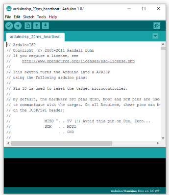
There is an official sketch (arduino program) for using the arduino as an ISP, it comes with the arduino installer as one of their File->Examples and is called ArduinoISP.
It's intended use is to use one arduino to reprogram other broked arduinos or make new ones from components. However we want to use it to pass along our own code, the FabISP firmware to our card. This is why the official instructions are only useful until step 5. After that you have to pice together your own tutorial from many different sources, that is why I wrote this one.
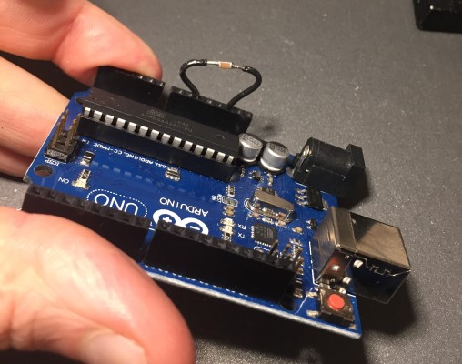
After we have uploaded the modified ArudinoISP sketch to our arduinio we had to add a 10 uF capacitor between reset and ground. Like this:
This has to do with the special way we will be using the arduino after we programmed it with the ArduinoISP sketch. Now we want to send code through it, not reprogram it. If we leave out the capacitor the arduino will interpret us sending code to it as an attempting to reprogram it and do an automatic reset, sending the code that we inteded for our FabISP to the arduino bootloader instead. If we include the capacitor, it absorbs the reset pulse and lets us send the code through the arduino to the FabISP card being programmed instead. Source
"The bootloader is basically a .hex file that runs when you turn on the board. It is very similar to the BIOS that runs on your PC. It does two things. First, it looks around to see if the computer is trying to program it. If it is, it grabs the program from the computer and uploads it into the ICs memory (in a specific location so as not to overwrite the bootloader). That is why when you try to upload code, the Arduino IDE resets the chip. This basically turns the IC off and back on again so the bootloader can start running again. If the computer isn’t trying to upload code, it tells the chip to run the code that’s already stored in memory. Once it locates and runs your program, the Arduino continuously loops through the program and does so as long as the board has power."
My emphasis Quote Source
(Arduino IDE = Arduino Integrated Development Environment or Arduino Software.)
TODO add comprehensive workflow guide and a guide to what is what and why is it there, especially about the jumpers.